Atomistic mechanism of graphene growth on SiC substrate: Large-scale molecular dynamics simulation based on a new charge-transfer bond-order type potential
Abstract
Thermal decomposition of silicon carbide is a promising approach for the fabrication of graphene. However, the atomistic growth mechanism of graphene remains unclear. This paper describes the development of a new charge-transfer interatomic potential. Carbon bonds with a wide variety of characteristics can be reproduced by the proposed vectorized bond-order term. Large-scale thermal decomposition simulation enables us to observe the continuous growth process of the multi-ring carbon structure. The annealing simulation reveals the atomistic process by which the multi-ring carbon structure is transformed to flat graphene involving only 6-membered rings. Also, it is found that the surface atoms of the silicon carbide substrate enhance the homogeneous graphene formation.
pacs:
68.65.-k, 82.20.Wt, 81.05.ueI Introduction
Graphene, a single-layer sheet of carbon (C) atoms, has many interesting characteristics Novoselov et al. (2004), including electronic and mechanical properties. Graphene is thus expected to have many applications for electronic devices Lin et al. (2010); Morozov et al. (2008); Bolotin et al. (2008). One of the promising methods for the fabrication of graphene is the thermal decomposition of silicon carbide (SiC) Berger (2006); Hibino et al. (2008); Virojanadara et al. (2008), because this method enables the graphene to be grown directly on a semi-insulating substrate without the need of a transfer process, which can induce defects in graphene. In order to obtain high quality and well-controlled graphene sheets, understanding the atomistic growth mechanism is essential.
The characteristics of the graphene depend on the surface orientation of SiC. On the Si-face of SiC, it is known that homogeneous, monolayer or multilayer graphene can be grown by controlling the growth conditions Norimatsu and Kusunoki (2009); Virojanadara et al. (2008); Emtsev et al. (2009). In this paper, we focus on the growth mechanics on the Si-face.
On the Si-face, the step of SiC plays an important role in the graphene growth mechanics Hibino et al. (2010); Hannon and Tromp (2008). HRTEM observations Norimatsu and Kusunoki (2010, 2014a) indicate that the initial stage of graphene is nucleated at the facet and grows to the terrace. Much of the experimental data Chen et al. (2005); Tsai et al. (1992); Seyller et al. (2006); Charrier et al. (2002); Rollings et al. (2006) shows that the graphene grown on the Si-face forms a honeycomb lattice consisting of graphene rings atop a SiC supercell. DFT calculations Varchon et al. (2008) indicate that the bottom layer of the graphene has a strong interaction with the SiC substrate. This is called the 0th layer or buffer layer.
To investigate the atomistic process of graphene growth, several studies with atomic-scale simulations have been performed Tetlow et al. (2014); Norimatsu and Kusunoki (2014b). A density functional theory (DFT) study based on geometrical optimization Kageshima et al. (2011, 2012) showed that graphene is formed on the SiC surface after C atoms are sufficiently accumulated on the surface. Another study simulated the formation of C clusters Inoue et al. (2012), and showed that the initial C cluster forms a penta-heptagonal structure (a multi-ring structure with 5- and 7-membered rings) rather than a purely hexagonal structure. The effect of the step was also investigated. Static energy calculations for a step model Kageshima et al. (2012) indicated that the aggregation of C atoms at the monolayer step edges of SiC reduces the energy of the system. Finally, a dynamics simulation in which Si atoms were removed at the facet one-by-one Morita et al. (2013) also suggested that the C multi-ring structure connected to the step edge is created at the nucleation stage.
To the best of our knowledge, all of the existing graphene growth simulation methods are based on the addition of excess C atoms or the removal of pre-selected Si atoms from SiC crystals. However, the thermal decomposition process is considered to be driven by the recombination of bonds at high temperature, which induces formation of the C cluster and desorption of Si atoms. In particular, the growing C cluster is considered to be stabilized by connecting to Si atoms Kageshima et al. (2012). A previous study Morita et al. (2013) showed that the removal of Si atoms from inappropriate positions has unexpected results. For example, the desorption of C atoms and the formation of a 3D-shaped C cluster were observed. Therefore, valid modeling of the desorption of Si atoms is essential in order to observe the graphene growth process until the C cluster completely covers the whole SiC surface.
In addition, the previous reports indicated that the penta-heptagonal structure is created at the initial stage of the graphene nucleation Inoue et al. (2012); Morita et al. (2013). This structure is considered to be transformed into an ideal graphene structure through the annealing process. The SiC substrate is thought to strongly affect the annealing process of graphene, since the bottom graphene layer is connected to SiC and has a reconstructed structure. However, these annealing processes have not yet been investigated by means of atomic-scale simulations. In order to see the process by which the initial inhomogeneous structure is transformed to ideal graphene through numerous bond recombinations, long-term and large-scale simulations are required. The DFT calculations in such simulations would have an extremely high computational cost, because of its scope of application. In this way, there is a large gap between the experiments and simulations.
The classical molecular dynamics (MD) scheme is considered to be an effective approach for these large-scale simulations. Indeed, several studies have simulated the structure of the graphene on SiC Lampin et al. (2010); Tang et al. (2008a) and the graphene growth process on SiC Tang et al. (2008b); Jakse et al. (2011) using MD. However, there have been no examples dealing with the continuous growth process of the C cluster, which takes care of the desorption of Si atoms. In order to reproduce the formation of the C cluster from the SiC substrate through the thermal decomposition using MD, it is necessary for the interatomic potential to express the changes in the nature of the bond accompanying the charge-transfer effect. This is because Si-C bonds in the SiC substrate have an ionic bond nature due to the difference of electronegativity, while the C cluster has pure covalent bonds. Also, the C atom shows various bonding nature and is stabilized in various allotropes, e.g., diamond, amorphous carbon and graphite. The formation of sparse structures such as C chains has also been reported in graphene growth simulations Morita et al. (2013); Ono et al. (2016). Therefore, the interatomic potential should reproduce the charge-transfer effect and various stable structures of C atoms. Currently, however, there are no interatomic potentials that meet both requirements.
II Methods
In our previous studies Takamoto et al. (2016); Kumagai et al. (2004), we developed a hybrid charge-transfer-type interatomic potential, based on the Tersoff potential, in order to reproduce the thermal oxidation of silicon. As compared to the other charge-transfer-type interatomic potential Yu et al. (2007); van Duin et al. (2003), this interatomic potential has the covalent-ionic mixed bond nature as expressed by in Takamoto et al. (2016). In this paper, we introduce a new interatomic potential that can reproduce the growth process of graphene on SiC substrate, within the framework of our hybrid charge-transfer interatomic potential. In addition, we propose an extended potential function without changing the philosophy of the Tersoff potential Tersoff (1986, 1988a, 1988b). We then incorporate a vectorized environmental-dependent function in order to reproduce various stable structures.
In the Tersoff-type potential, the bond order term is calculated as
| (1) |
where and are potential parameters. is a many-body term which expresses the dependence of bond order on the coordination number and bond angle. In the Tersoff-type potential, ( for bond ) is calculated as the summation of a function of atoms and with respect to the surrounding atoms , as shown in Eq. (2). The form is
| (2) |
where F is a function, , and are the bond lengths and angles of atoms and . Here, we call a surrounding environment function.
In this paper, we have vectorized the surrounding environment function . In other words, we have defined the bond order as a function of the independent terms . Each () is expected to express the respective bonding nature. For example, corresponds to the structure with a high-coordination number, while corresponds to that with a low-coordination number.
In this paper, the bond order is defined by the following forms:
| (3) | ||||
| (4) | ||||
| (5) |
where , p, and are potential parameters which take positive values. is a normalization constant so that is equal to in the case that there are no surrounding atoms (which means for all ). Equation 4 means is calculated as the -norm of . In the extreme case of , is equal to the minimum value among and other are ignored. In this case, is rewritten as
| (6) |
Then, we obtained the original Tersoff-type bond order form in the braket. That means the interatomic potential can select the most stable bonding nature among various . In the case of , on the other hand, becomes the geometric mean, which means that the interatomic potential shows a mixed bond nature.
The entire potential function form is shown in our previous paper Takamoto et al. (2016). In this paper, the bond order is calculated by the newly introduced function (Eq. (3)). We fix to 2. We show the function in the expanded form below.
| (7) |
where , , , , and are the potential parameters. is a normalization constant so that the maximum of will be 1. In this work, we fix to 2. The surrounding environment function is calculated in the same way as of the previous paper Takamoto et al. (2016).
The atomic charge varies in response to its environment so as to minimize the total energy . The conjugate gradient method is used to minimize the energy. The charge is minimized in every timestep. In addition, the constant energy term is added to the self energy term to improve the energy representations of various structures. This interatomic potential is implemented in the LAMMPS Molecular Dynamics Simulator Plimpton (1995); lam .
We fit the potential parameters by our potential-making scheme Takamoto et al. (2016); Kumagai and Izumi (2011). We use various snapshots obtained by MD as a training dataset for fitting. DFT calculations were performed using the first-principles electronic structure calculation program “PHASE/0” nim ; Ohno et al. (2007). We used the local density approximation (LDA). We typically used Monkhorst-Pack k-point grids. The cutoff of plane-wave basis set is 980 eV/atom. The number of fitted properties is about 260,000. The properties used for the fitting are energies, atomic forces and atomic charges.
For C cluster fitting, snapshots of diamond, amorphous, liquid, graphene, graphite, and multi-rings with 6-membered rings, single rings with various numbers of atoms and chain structures are sampled. The mixed structures consisting of diamond, 6-membered rings and chains are also sampled. The same structures are used for Si fitting. For Si-C system fitting, the following structures were prepared: various SiC crystals, diamond-like structures in which the Si and C atoms are assigned to each site of the diamond lattice in various patterns, diamond-like structures with vacancies, diamond-like structures with surfaces, C clusters on the surface of SiC crystals, flat graphene-like SiC structures and chain structures. DFT-MD calculations were also performed to sample the structrures of C clusters on the SiC crystals.
III Representation of the interatomic potential
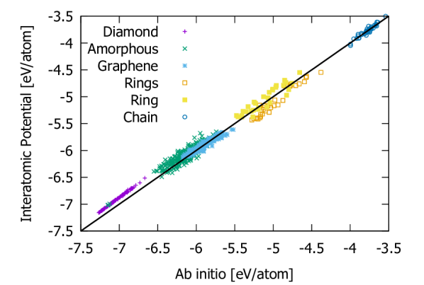
Figure 1 plots the comparison of energies between DFT calculation and the fitted interatomic potential for snapshots of typical structures (diamond, amorphous, graphene, multi-ring, single ring, chain) used for the fitting process. The fitted interatomic potential well reproduces the structures with a wide-range of coordination numbers.
Next, we verify the effect of the vectorized surrounding environment function . We created interatomic potentials in which one of is doubled in order to suppress the corresponding bond nature artificially. The energy comparisons are shown in Fig. 2.
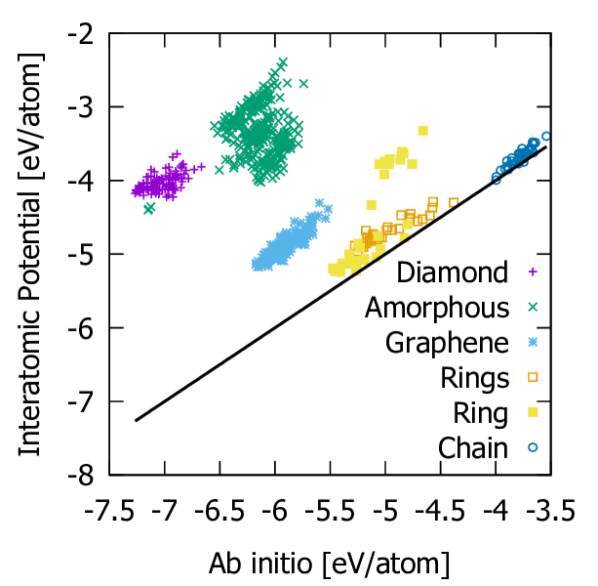
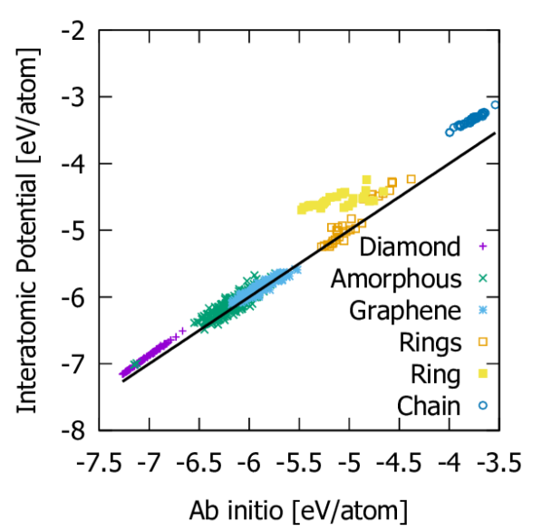
The interatomic potential in which is suppressed well reproduces the structures with low coordination numbers (e.g., ring and chain), while it has poor energy reproducibility for the structures with high coordination numbers (e.g., diamond and graphene). On the other hand, the interatomic potential in which is suppressed shows the opposite tendency. Also, the minimum bond angle of is and that of is .
Next, we verified the reproducibility of sparse structures. We created a 16-membered single C ring structure and annealed it at 2500 K. Although the structure of our interatomic potential kept its ring network, that of the Tersoff-type potential Tersoff (1994) was transformed into a cage-like high density structure. The DFT study showed that the ring structure with 16 carbon atoms was more stable than the cage-like structure Jones (1999).
To validate the applicability of the interatomic potential for the interaction between graphene and SiC, we created a large structure with graphene on the surface of SiC and compared with the previous studies. As described in the Introduction section, the graphene on the Si-face of SiC is considered to form a structure. We overlaid a graphene hexagon structure onto a 4H-SiC supercell. It is noted that this structure is not used for the fitting process.
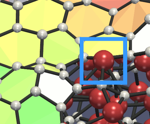
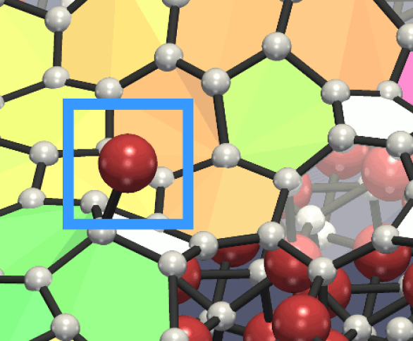
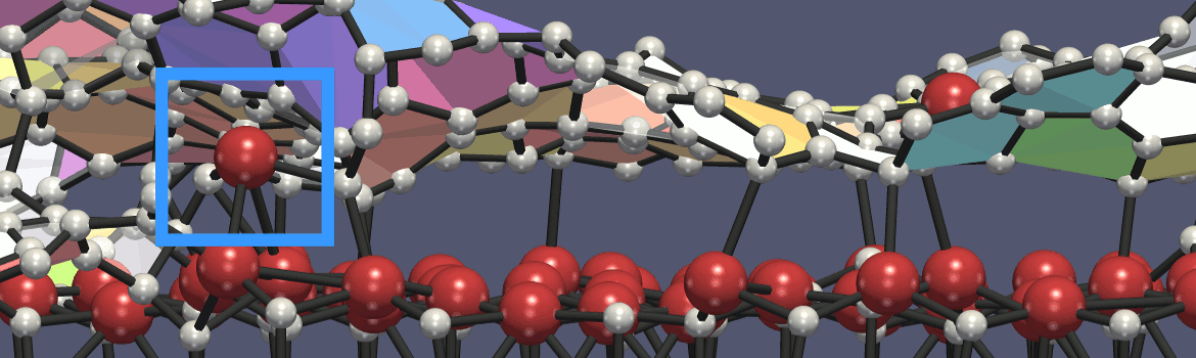
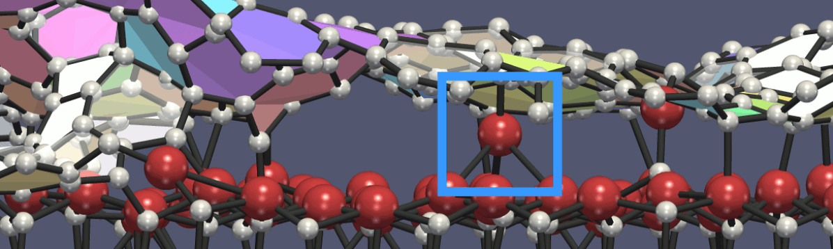
The structure after energy minimization is shown in Fig. 3 (top view: (3); side view: (3)). The color of Fig. 3(3) shows the vertical position of the C atoms from the bottom of the MD cell.
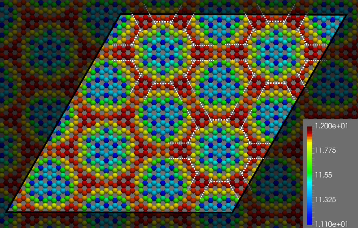
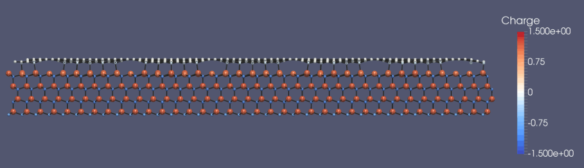
From Fig. 3(3), there are two types of C atoms. One is connected to Si atoms of SiC and the other is not. This result is consistent with the previous experiment Chen et al. (2005) and DFT Varchon et al. (2008) studies. The difference in height between the lowest and highest C atoms is about 1.0 . This value is also close to the DFT result Varchon et al. (2008) (1.2 ). From Fig. 3(3), we clearly see the long-range hexagonal pattern, which is also seen in the STM image and DFT calculation Varchon et al. (2008). As seen by the white dashed line in Fig. 3(3), there were two types of hexagonal patterns (isotropic ones and triangle ones), which were pointed out in the previous study Lampin et al. (2010). Therefore, out interatomic potential reproduces the interactions between SiC and graphene.
IV Graphene growth simulation
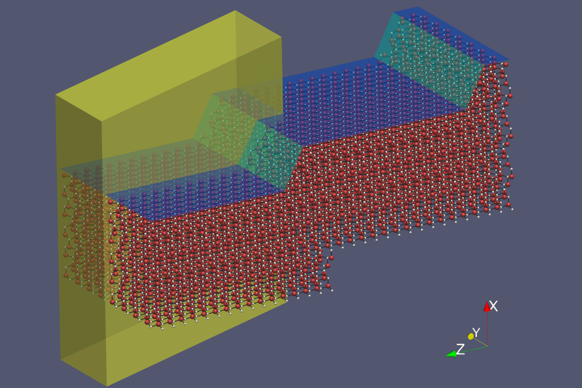
In order to simulate the dynamics of graphene growth process caused by thermal desorption of Si atoms, we carried out MD simulation. We have prepared a periodic step structure as shown in Fig. 4. Two MD cells are displayed along the Y and Z directions. The substrate is 4H-SiC. The surface orientations of the terrace and facet are and , respectively. The terrace and facet faces are shown in blue and green planes. The height of the facet is one layer of the 4H-SiC lattice (4 bilayer). As indicated by the yellow box in Fig. 4, the MD cell is tilted so that the upper and lower terraces are smoothly connected without any steps through the periodic boundary. The total number of atoms in the single MD cell is about 12,000.
In this simulation, the desorption of Si atoms is modeled by gradually removing instable Si atoms on the surface during MD. The stability of Si atoms is measured by the total energy change following the elimination of that atom at every 1 ps. The threshold of removing Si atoms is set to be 6.5 eV. In this simulation, the energy to remove a typical Si atom on the terrace is about 10 eV. Therefore, the Si atoms whose energy is 3.5 eV higher than that of Si atoms on the terrace are removed. In this manner, the order and timing of Si atoms to be removed are not set in advance.
We carried out MD with NVT ensemble at 2500 K while fixing the bottom of SiC. It is noted that the experimental temperature for growth process is typically between 1473 K and 1933 K Tetlow et al. (2014), and the growth timescale is the order of minutes.
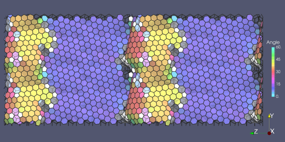
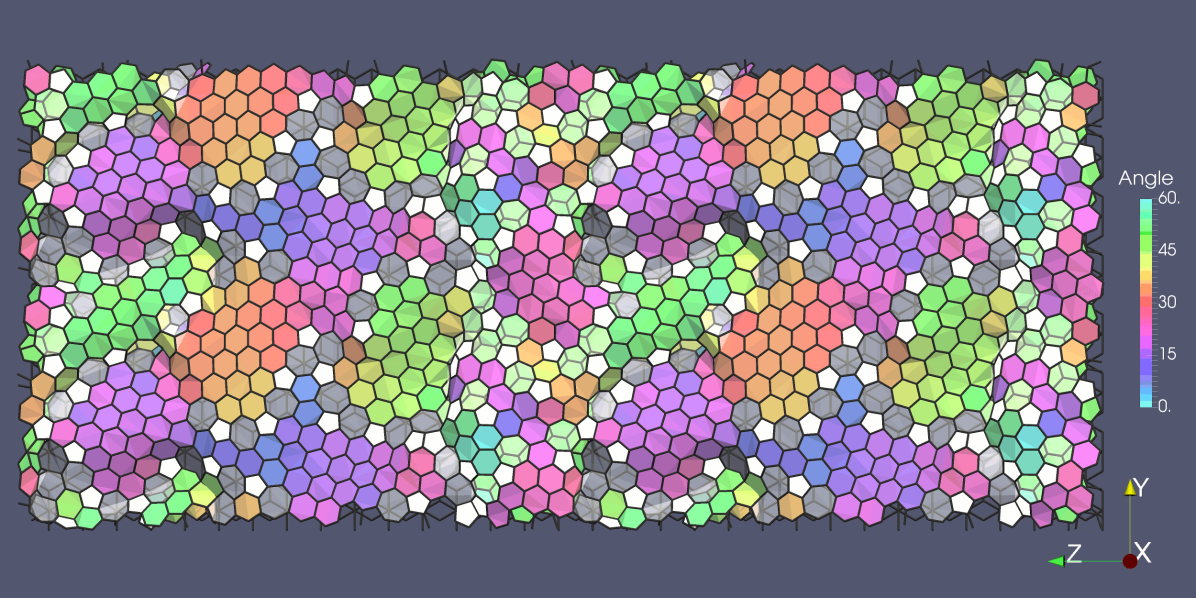
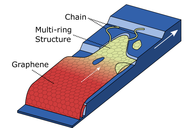
The results are shown in Fig. 6. Here, we illustrate C rings as films. 7 or 8-membered rings are shown in (semitransparent) gray and 3,4 or 5-membered rings are shown in white. The hue of the 6-membered ring expresses its in-plane orientation. The hue makes one lap at 60 degrees rotation. The orientation is zero in the case that one pair of the diagonal vertex is directed to . We also illustrate C chains as white lines. The left figures are top views of the rings, chains and bonds. The right figures are side views in which atoms are shown in addition to the rings, chains and bonds. The dashed white lines show the initial position of the surface.
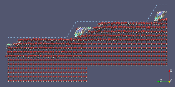
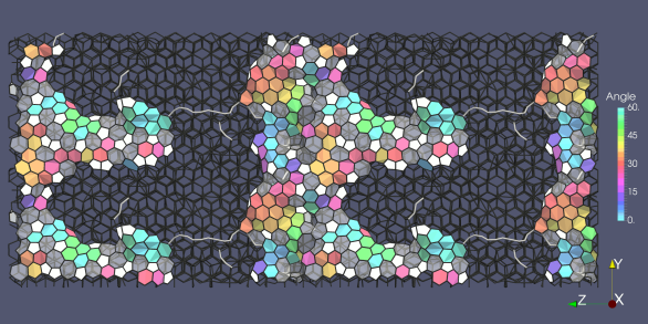
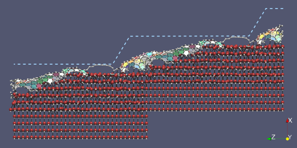
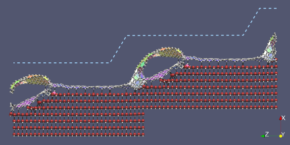
The graphene growth proceeded as follows. Figure 6(6): Desorption of Si atoms from the facet is observed. As the number of C atoms on the facet increases, a striped multi-ring structure is formed. The bottom of the C cluster is vertically bonded to the SiC. While the total number of the rings is less than 20, the numbers of 5-membered rings and 6-membered rings are increased in the same way as in the previous study Morita et al. (2013).
Figure 6(6): After the formation of the C cluster on the facet face, the desorption of Si atoms at the edge of the upper terrace starts and creates one-bilayer steps. The excess C atoms move on the terrace actively and connect to the C cluster. As a result, the C multi-ring structure is formed on the terrace. C chains connected to the C cluster are also seen on the terrace. The C multi-ring structure on the terrace is connected to the edge of the step of the SiC bilayer. It is noted that the top bilayer also consists of 6-membered rings and it can smoothly connect to the C multi-ring structure. Also, the aggregation of C atoms forms a C-rich area and Si-rich area. In Fig. 6(6), the shape of the C cluster is wavy. This shape is similar to the finger-like structures of graphene observed by AFM Borovikov and Zangwill (2009). However, caution should be taken when making a direct comparison, because this structure has a ten-nanometer scale, while the observed finger-like structures have a micrometer scale.
V Discussion
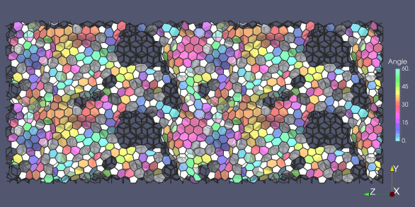
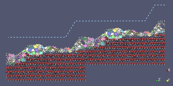
The obtained structure involves the roughness due to many 5 and 7-membered rings, which is similar to the previous DFT results Inoue et al. (2012). In addition, the structure is inhomogeneous and contains thick areas and holes. It is considered that the structure is transformed into a perfect graphene structure by the additional annealing process. Therefore, the structure is annealed at 3000 K NVT ensemble for 12.8 ns. After the annealing simulation, we relaxed the structure. The annealed structure is shown in Fig. 6. The time histories for the numbers of 5, 6, and 7-membered rings are shown in Fig. 7. The annealing starts at 3.2 ns (vertical line in the figure).
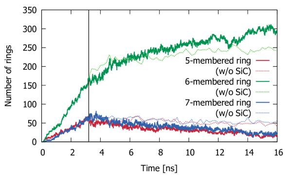
During the annealing, the number of 6-membered rings is increased and those of 5 and 7-membered rings are decreased. The diffusion of C atoms makes the density of C atoms uniform. As a result, a flat, graphene-like structure was obtained on the terrace, while a double layer structure was created on the facet due to excess C atoms. In particular, a perfect and flat graphene structure composed of 6-membered rings was formed on the terrace.
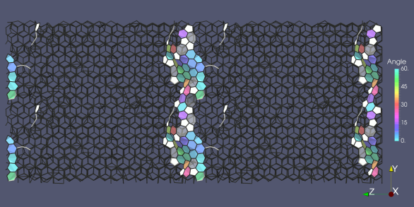
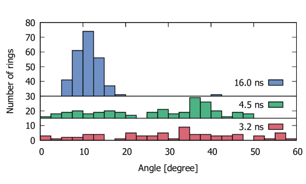
Histograms of the orientations of 6-membered rings on the terrace after 3.2, 4.5 and 16.0 ns are shown in Fig. 8. Zero degrees corresponds to the structure. At the initial stage (4.5 ns), the largest graphene piece orients . However, the further annealing gradually shrinks this orientation region. The surface atoms of the SiC substrate are likely to affect this process since deviates from the stable orientation. The peak of after 16 ns would be caused by the artificial periodic boundary conditions because it limits the possible orientation and prevents the rotation of the structure.
In order to investigate the effect of the SiC substrate on the formation of graphene, we created a “free-standing C cluster film” model by eliminating SiC from the 3.2 ns structure (Fig. 6(6)). After the same-condition annealing, the structure shown in Fig. 9 was obtained. The time histories for the numbers of 5, 6, and 7-membered rings are also shown in Fig. 7 (the lines labeled “w/o SiC”). It can be seen that the region of 6-membered rings is divided into small pieces and its orientation is not uniform. During the annealing, the number of 5 and 7-membered rings is decreased by 20 %, while it is decreased by 80 % in the case of graphene with SiC. Therefore, it is considered that the SiC substrate enhances the recombination of C-C bonds and resulting homogeneous formation. This would be similar to the graphene growth on metals. The calculated reaction barrier to healing a Stone-Wales defect on an Ni Jacobson et al. (2012) is 2.88 eV, which is lower than that for free-standing graphene (4.10 eV).
It is noted that Si atoms frequently move as readily as C atoms. During the annealing simulation, we observed that several Si atoms were ejected to the surface side of the C cluster film through a hole, and were diffused along the SiC-graphene interface. The snapshots of these events are shown in Fig. 10. These results indicate that the thermal decomposition of SiC continues even after the surface is covered by the graphene.
The graphene growth model suggested from these results is shown in Fig. 11. After the formation of the C cluster at the facet, the desorption of Si atoms starts at the upper terrace. The excess C atoms move actively on the SiC and form multi-ring structures. These processes are consistent with the model inferred by the earlier experimental work Norimatsu and Kusunoki (2010). The initial C cluster is not uniform and contains many 5 and 7-membered rings. The SiC surface enhances the bond recombinations of the C cluster and the formation of the perfect graphene. It should be noted that the graphene growth mode may depend on the direction and height of the step and crystal polymorphism Dojima et al. (2016). Investigation of those effects is a future work.
VI Conclusion
A new charge-transfer interatomic potential is developed in order to reproduce the formation and homogenization of graphene on the SiC by thermal decomposition. A new bond order function based on a vectorized surrounding environment parameter is proposed to reproduce various bond nature of C atoms.
The large-scale thermal decomposition simulation reproduces the continuous growth process of the C multi-ring structure on the terrace. The annealing simulation reveals the atomistic process of the transformation of the C multi-ring structure to flat graphene involving only 6-membered rings. Also, it is found that the surface atoms of the SiC substrate enhance the homogeneous graphene formation.
Acknowledgements.
A portion of this research was partly supported by MEXT within the priority issue 6 of the FLAGSHIP2020 and JSPS KAKENHI Grant No. 16H03830. The DFT-MD calculations were carried out on the K computer provided by RIKEN, AICS through the HPCI System Research project (Project ID:hp150266 and hp160226). This work was supported by a Grant-in-Aid for JSPS Research Fellow.References
- Novoselov et al. (2004) K. S. Novoselov, A. K. Geim, S. V. Morozov, D. Jiang, Y. Zhang, S. V. Dubonos, I. V. Grigorieva, and a. a. Firsov, Science (New York, N.Y.) 306, 666 (2004), arXiv:0410550 [cond-mat] .
- Lin et al. (2010) Y.-M. Lin, C. Dimitrakopoulos, K. A. Jenkins, D. B. Farmer, H.-Y. Chiu, A. Grill, and P. Avouris, Science (New York, N.Y.) 327, 662 (2010), arXiv:1002.3845 .
- Morozov et al. (2008) S. V. Morozov, K. S. Novoselov, M. I. Katsnelson, F. Schedin, D. C. Elias, J. A. Jaszczak, and A. K. Geim, Physical Review Letters 100, 016602 (2008), arXiv:0710.5304 .
- Bolotin et al. (2008) K. Bolotin, K. Sikes, Z. Jiang, M. Klima, G. Fudenberg, J. Hone, P. Kim, and H. Stormer, Solid State Communications 146, 351 (2008), arXiv:0802.2389 .
- Berger (2006) C. Berger, Science 312, 1191 (2006).
- Hibino et al. (2008) H. Hibino, H. Kageshima, F. Maeda, M. Nagase, Y. Kobayashi, and H. Yamaguchi, Physical Review B 77, 075413 (2008), arXiv:0710.0469 .
- Virojanadara et al. (2008) C. Virojanadara, M. Syväjarvi, R. Yakimova, L. I. Johansson, A. A. Zakharov, and T. Balasubramanian, Physical Review B 78, 245403 (2008).
- Norimatsu and Kusunoki (2009) W. Norimatsu and M. Kusunoki, Chemical Physics Letters 468, 52 (2009).
- Emtsev et al. (2009) K. V. Emtsev, A. Bostwick, K. Horn, J. Jobst, G. L. Kellogg, L. Ley, J. L. McChesney, T. Ohta, S. a. Reshanov, J. Röhrl, E. Rotenberg, A. K. Schmid, D. Waldmann, H. B. Weber, and T. Seyller, Nature Materials 8, 203 (2009), arXiv:arXiv:0903.2067v1 .
- Hibino et al. (2010) H. Hibino, H. Kageshima, and M. Nagase, Journal of Physics D: Applied Physics 43, 374005 (2010).
- Hannon and Tromp (2008) J. B. Hannon and R. M. Tromp, Physical Review B 77, 241404 (2008).
- Norimatsu and Kusunoki (2010) W. Norimatsu and M. Kusunoki, Physica E: Low-dimensional Systems and Nanostructures 42, 691 (2010).
- Norimatsu and Kusunoki (2014a) W. Norimatsu and M. Kusunoki, Journal of Physics D: Applied Physics 47, 094017 (2014a).
- Chen et al. (2005) W. Chen, H. Xu, L. Liu, X. Gao, D. Qi, G. Peng, S. C. Tan, Y. Feng, K. P. Loh, and A. T. S. Wee, Surface Science 596, 176 (2005).
- Tsai et al. (1992) M.-H. Tsai, C. S. Chang, J. D. Dow, and I. S. T. Tsong, Physical Review B 45, 1327 (1992).
- Seyller et al. (2006) T. Seyller, K. Emtsev, K. Gao, F. Speck, L. Ley, A. Tadich, L. Broekman, J. Riley, R. Leckey, O. Rader, A. Varykhalov, and A. Shikin, Surface Science 600, 3906 (2006).
- Charrier et al. (2002) A. Charrier, A. Coati, T. Argunova, F. Thibaudau, Y. Garreau, R. Pinchaux, I. Forbeaux, J.-M. Debever, M. Sauvage-Simkin, and J.-M. Themlin, Journal of Applied Physics 92, 2479 (2002).
- Rollings et al. (2006) E. Rollings, G.-H. Gweon, S. Zhou, B. Mun, J. McChesney, B. Hussain, A. Fedorov, P. First, W. de Heer, and A. Lanzara, Journal of Physics and Chemistry of Solids 67, 2172 (2006), arXiv:0512226 [cond-mat] .
- Varchon et al. (2008) F. Varchon, P. Mallet, J.-Y. Veuillen, and L. Magaud, Physical Review B 77, 235412 (2008).
- Tetlow et al. (2014) H. Tetlow, J. Posthuma de Boer, I. J. Ford, D. D. Vvedensky, J. Coraux, and L. Kantorovich, Physics Reports 542, 195 (2014), arXiv:1602.06707 .
- Norimatsu and Kusunoki (2014b) W. Norimatsu and M. Kusunoki, Semiconductor Science and Technology 29, 064009 (2014b).
- Kageshima et al. (2011) H. Kageshima, H. Hibino, H. Yamaguchi, and M. Nagase, Japanese Journal of Applied Physics 50, 095601 (2011).
- Kageshima et al. (2012) H. Kageshima, H. Hibino, and S. Tanabe, Journal of Physics: Condensed Matter 24, 314215 (2012).
- Inoue et al. (2012) M. Inoue, H. Kageshima, Y. Kangawa, and K. Kakimoto, Physical Review B 86, 085417 (2012).
- Morita et al. (2013) M. Morita, W. Norimatsu, H.-J. Qian, S. Irle, and M. Kusunoki, Applied Physics Letters 103, 141602 (2013).
- Lampin et al. (2010) E. Lampin, C. Priester, C. Krzeminski, and L. Magaud, Journal of Applied Physics 107, 103514 (2010), arXiv:0912.2034 .
- Tang et al. (2008a) C. Tang, L. Meng, L. Sun, K. Zhang, and J. Zhong, Journal of Applied Physics 104, 113536 (2008a).
- Tang et al. (2008b) C. Tang, L. Meng, H. Xiao, and J. Zhong, Journal of Applied Physics 103 (2008b), 10.1063/1.2894728.
- Jakse et al. (2011) Jakse, Arifin, and Lai, Condensed Matter Physics 14, 43802 (2011), arXiv:arXiv:1202.4846v1 .
- Ono et al. (2016) Y. Ono, T. Yamasaki, J. Nara, and T. Ohno, in NT16 The 17th International Conference on the Science and Application of Nanotubes (2016) pp. 165–166.
- Takamoto et al. (2016) S. Takamoto, T. Kumagai, T. Yamasaki, T. Ohno, C. Kaneta, A. Hatano, and S. Izumi, Journal of Applied Physics 120, 165109 (2016).
- Kumagai et al. (2004) T. Kumagai, S. Izumi, S. Hara, and S. Sakai, in Extended Abstracts of International Conference on Computational Methods (2004) p. 75.
- Yu et al. (2007) J. Yu, S. B. Sinnott, and S. R. Phillpot, Physical Review B 75, 085311 (2007).
- van Duin et al. (2003) A. C. T. van Duin, A. Strachan, S. Stewman, Q. Zhang, X. Xu, and W. A. Goddard, The Journal of Physical Chemistry A 107, 3803 (2003).
- Tersoff (1986) J. Tersoff, Physical Review Letters 56, 632 (1986).
- Tersoff (1988a) J. Tersoff, Physical Review B 37, 6991 (1988a).
- Tersoff (1988b) J. Tersoff, Physical Review Letters 61, 2879 (1988b).
- Plimpton (1995) S. Plimpton, Journal of Computational Physics 117, 1 (1995).
- (39) The implementation and parameters are available at https://github.com/Takamoto-So/tersoff_k2.
- Kumagai and Izumi (2011) T. Kumagai and S. Izumi, Transactions of the Japan Society of Mechanical Engineers A, 77, 2026 (2011), (in Japanese).
- (41) “NIMS / nano-simulation software,” https://azuma.nims.go.jp.
- Ohno et al. (2007) T. Ohno, T. Yamamoto, T. Kokubo, A. Azami, Y. Sakaguchi, T. Uda, T. Yamasaki, D. Fukata, and J. Koga, in Proceedings of the 2007 ACM/IEEE Conference on Supercomputing, SC ’07 (ACM, New York, NY, USA, 2007) pp. 57:1–57:6.
- Tersoff (1994) J. Tersoff, Physical Review B 49, 16349 (1994).
- Jones (1999) R. O. Jones, The Journal of Chemical Physics 110, 5189 (1999).
- Borovikov and Zangwill (2009) V. Borovikov and A. Zangwill, Physical Review B 80, 121406 (2009), arXiv:0907.1606 .
- Jacobson et al. (2012) P. Jacobson, B. Stöger, A. Garhofer, G. S. Parkinson, M. Schmid, R. Caudillo, F. Mittendorfer, J. Redinger, and U. Diebold, The Journal of Physical Chemistry Letters 3, 136 (2012).
- Dojima et al. (2016) D. Dojima, Y. Kutsuma, K. Ashida, and T. Kaneko, in The European Conference on Silicon Carbide and Related Materials (2016) pp. 609–610.