22email: lijian16@nudt.edu.cn 33institutetext: J. T. Santos 44institutetext: Department of Applied Physics, Aalto University, P.O. Box 15100, FI-00076 AALTO, Finland 55institutetext: M. A. Sillanpää 66institutetext: Department of Applied Physics, Aalto University, P.O. Box 15100, FI-00076 AALTO, Finland
High precision displacement sensing of monolithic piezoelectric disk resonators using a single-electron transistor
Abstract
A single electron transistor (SET) can be used as an extremely sensitive charge detector. Mechanical displacements can be converted into charge, and hence SETs can become sensitive detectors of mechanical oscillations. For studying small-energy oscillations, an important approach to realize the mechanical resonators is to use piezoelectric materials. Besides coupling to traditional electric circuitry, the strain-generated piezoelectric charge allows for measuring ultrasmall oscillations via SET detection. Here we explore the usage of SETs to detect the shear mode oscillations of a diameter quartz disk resonator with a resonance frequency around . We measure the mechanical oscillations using either a conventional dc SET, or use the SET as a homodyne or heterodyne mixer, or finally, as a radio-frequency single-electron transistor (RF-SET). The RF-SET readout is shown to be the most sensitive method, allowing us to measure mechanical displacement amplitudes below meters. We conclude that a detection based on a SET offers a potential to reach the sensitivity at the quantum limit of the mechanical vibrations.
Keywords:
Single Electron Transistor Piezoelectric Resonators Displacement Detectors1 Introduction
The measurement of atto-Newton forces, or sub-Ångstrom displacements, has a wide range of existing or potential applications, from magnetic resonance force microscopy slides to the study of frontiers of physics such as gravitational waves or quantum effects in the motion of mechanical resonators Palomaki710 ; Wollman952 ; JuhaSqueeze ; Lecocq2015 . Magnetomotive Cleland1996 ; Cleland1999256 ; Mohanty2000 ; Pashkin08 , optical interferometric Carr1999 ; Hakseong2017 as well as mixing vanderZant2009 ; Bachtold2009 detection techniques have been widely utilized in fundamental research. Moreover, we mention approaches that base on the concept of cavity optomechanics, where the mechanical oscillations affect the electromagnetic fields inside either an optical Cohadon1999 ; Aspelmeyer2006cool ; Heidmann2006 or an electrical Lehnert2008Nph resonator.
The original detection approaches used in fundamental research included, for instance, the magnetomotive technique that however, suffers from the need of high fields and bulky equipment. Similarly, optical interferometry also endures the latter issue, and the laser spot size limits the size of the mechanical resonator that can be studied. While impressive quantum experiments have been performed using cavity optomechanics either in optical or in microwave frequency range, the laser or microwave powers that are needed tend to be high and heat up the system. Therefore, one should look for even less intrusive detection techniques that would work at extremely small power. To this end, several experiments have taken advantage of a single electron transistor (SET) Flees1997 ; Joyez1994 , which is an ultimate charge sensitive device, and can be capacitively coupled to mechanical devices Knobel2003 ; LaHaye74 ; Nakamura2010nems . In such scheme, a dc voltage bias of the order of several volts is applied to a conductive mechanical resonator, and the mechanical vibrations modulate the amount of charge coupled to the SET. In the most delicate measurements, the SET has been replaced by superconducting qubits that bring the system in the quantum regime LaHaye2009 ; ClelandMartinis ; transmonnems ; LSETNEMSexp ; Delsing2014 ; LaHaye2016 .
In our recent work Santos2017 , we show how a massive piezoelectric resonator coupled to superconducting microcircuits woolley2016 can be analyzed as a cavity optomechanical device, with implications in studies of quantum-mechanical phenomena. The sensitivity advantage offered by piezoelectric transduction Knobel2003 ; Knobel2002 ; Sidles91 is highly beneficial for studying and further using the quantum properties of truly macroscopic resonators that can exhibit long energy lifetimes but nearly vanishing amplitudes of their zero-point motion.
In practical usage, a SET has a very limited bandwidth. The typical large tunnel junction resistance needed for the Coulomb blockade, together with the ever present stray capacitance from the cables limits the output bandwidth to about . A first stage amplifier in close proximity to the SET Pettersson96 ; Visscher96 can extend the bandwidth to Hz at best. There are two standard options to circumvent this limitation and broaden the spectral range of the SET. One is to use it as a radio-frequency (RF) mixer, either in homodyne, or in heterodyne measurement scheme knobel81 ; Abuelmaatti2009 , taking advantage of the nonlinear dependence of the SET current response to the gate charge. This approach does not increase the instantaneous bandwidth of the SET, which is still limited by the RC charging time, but allows to tune the measurement center frequency up to knobel81 . The second approach is to use an RF-SET Schoelkopf1238 , where a series inductance resonates with the cable stray capacitance, creating an LC tank resonator that impedance matches the SET to the low impedance cables, unlocking bandwidth up to Devoret2000 .
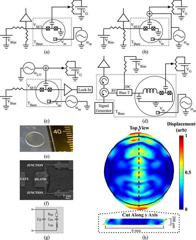
In this article we investigate a mechanical system that is a 6 millimetre diameter and 200 microns thick quartz disk resonator (Fig. 1e) that has the first shear mode resonance frequency at . A major motivation for studying such monolithic resonators is that they can have exceedingly high mechanical quality factors, paving the way towards macroscopic quantum mechanics goryachev2012 . These systems are truly macroscopic with the mode effective mass around 20 mg. We study the prospect of measuring the disk vibrations using four different SET detection setups: DC (Fig. 1a), homodyne mixing (Fig. 1b), heterodyne mixing (Fig. 1c), and RF-SET (Fig. 1d). The SETs are fabricated directly on top of the quartz disk (Fig. 1f), that acts as both the mechanical element and the substrate for the fabrication of the electrical circuit. The basic idea is independent of the measurement scheme chosen: the deformation of the quartz disk generates piezoelectric charge on the chip surface; the charge created in the vicinity of the SET island couples to it, thereby modulating the tunnelling current or the SET resistance.
2 Piezoelectric Resonator and SET
A piezoelectric resonator can be represented by an equivalent series RLC circuit like the one in Fig. 1g. Let us consider a circular quartz disk with the surface area , thickness , shear mode stress coefficient , shear modulus , relative permittivity , and piezoelectric coupling coefficient . The geometric capacitance in the plate-capacitor approximation is and the other equivalent circuit parameters can be calculated as , and , where is the mechanical quality factor. In Table 1, we summarize the quantities mentioned above.
| Parameter | Symbol | Value | Unit |
|---|---|---|---|
| Disk Surface Area | |||
| Disk Thickness | |||
| Quartz Shear Modulus | |||
| Quartz Shear Stress Coefficient | |||
| Quartz Relative Permittivity | |||
| Disk Mechanical Frequency | |||
| Coupling Coefficient | |||
| Geometric capacitance | |||
| Mechanical capacitance | |||
| Mechanical inductance | |||
| Mechanical resistance | |||
| Mechanical quality factor |
A static shear deformation corresponding to an applied potential difference between the two faces of the quartz disk is given as
| (1) |
that amounts to less than a nanometer displacement per volt. In a dynamical situation, close to the mechanical resonance, the resonator amplifies the applied voltage with the frequency , cf. the equivalent electrical circuit in Fig. 1g, and one obtains the dynamical vibration amplitude
| (2) |
where
| (3) |
and ms-1 is the sound speed of shear waves in quartz.
In the experiment, we actuate the vibrations through a separate excitation electrode shown in Fig. 1a-d. Equation (2) holds only for the part of the chip covered by the excitation electrode, while we are interested in the amplitude under the SET island somewhat distant from the electrode. In order to enable experimental comparison, we need to know how much the amplitude is reduced from that in Eq. (2) due to the small overlap. To this end we run a Comsol simulation and compare a full electrode coverage versus the actual chip layout, obtaining a reduction factor that should multiply the right-hand-side of Eq. (2).
Assuming a uniform piezoelectric charge distribution across the disk surface, a shear deformation corresponds to a shear strain and generates a piezoelectric surface charge density . Then, the number of electron charges coupled to a SET island is
| (4) |
Here, is the effective quartz surface area over which the SET sees the piezo charge. It is of the order the SET island area, but larger by a small numerical factor.
We model the SET response to charge as follows. If there is a total charge coupled to the SET island, we suppose the periodic gate charge response of the SET can be approximated as sinusoidal:
| (5) |
which represents the periodicity of a superconducting SET. Here, is the peak-to-peak amplitude of gate modulation, and the average current, both of which depend on the SET bias. The nonlinearity of the SET is the basis for the DC and mixing detection methods. The most general case of gate charge setting discussed below consists of three terms. There is usually a non-zero constant offset , and around the offset the gate charge is supposed to oscillate sinusoidally in time due to the mechanical oscillations driven at the frequency . Moreover, in the mixing schemes, there is a strong local oscillator at the frequency and with the amplitude :
| (6) |
The nested sinusoidal behaviour of Eqs. (5,6) will be seen in the experimental data below.
3 Results
In the measurements, we used two individual samples, labeled A and B. Sample A was used in all the other measurements except in the heterodyne scheme (Fig. 1c). The samples were essentially similar, but sample B had a smaller junction resistance, although this plays only a minor quantitative role in the results.
We begin with discussing the current-voltage (IV) properties of the SET in sample A. It comprises a island delimited by two Al () / AlOx / Al () tunnel junctions made by shadow evaporation. For the measurements, the edges of the chip with the SET are firmly glued to a sample stage, but the center of the chip is free to vibrate. All the measurements discussed in this paper were carried out in a dilution refrigerator at a temperature of mK. The sum resistance of the two junctions of our SET in sample A is approximately , and the charging energy is estimated as 0.3 K.
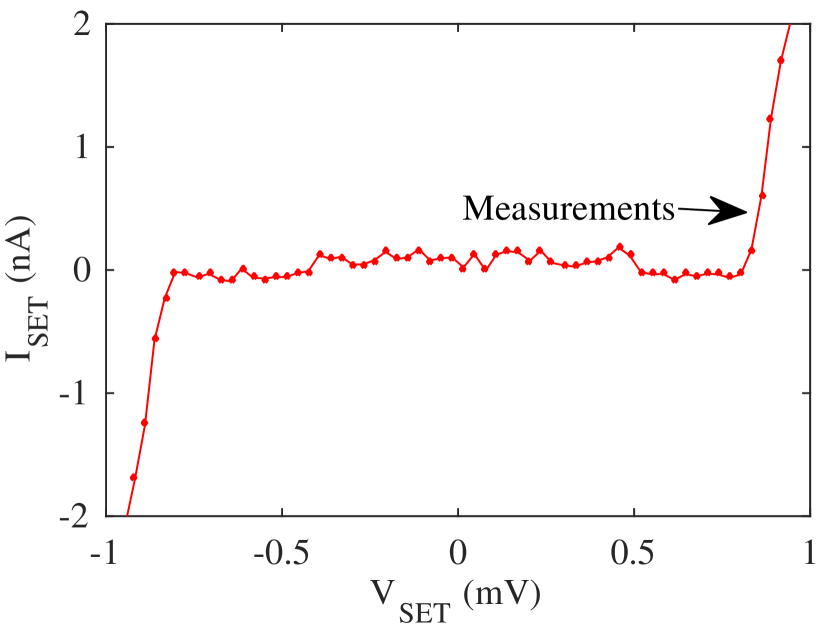
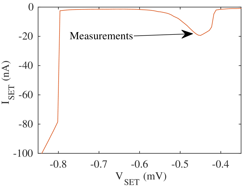
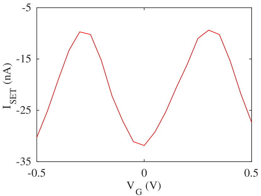
The standard DC IV measurement involves the biasing scheme shown to the left in Figs. 1a-c. We apply current bias through a resistor for the schemes in Figs. 1a-b and through in Fig. 1c. Figure 2(a) shows the DC IV properties for our SET device. The width of the current plateau is mostly set by the superconductor gap in our superconducting device. The Coulomb blockade modulation as a function of the gate voltage is visible at edges of the plateau.
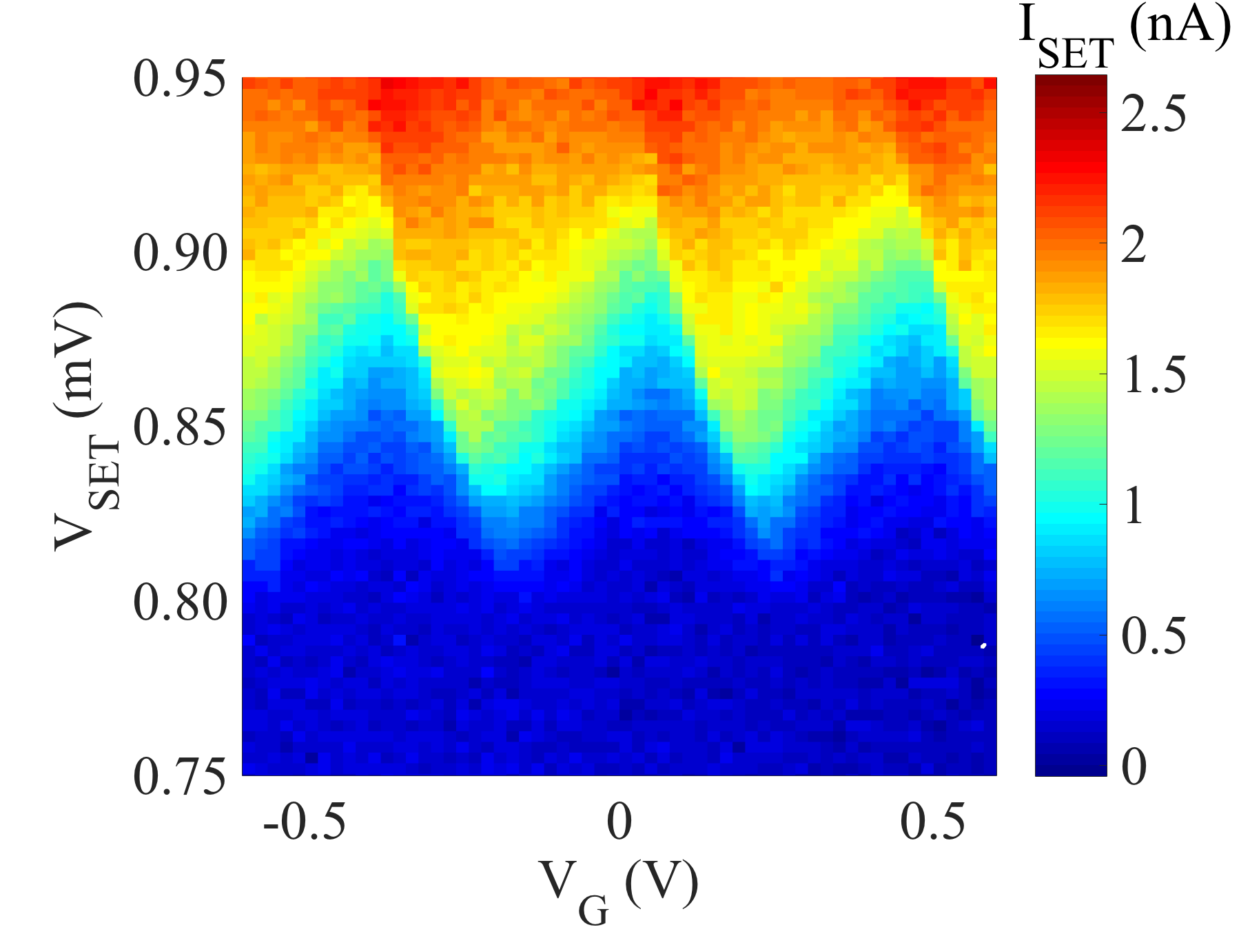
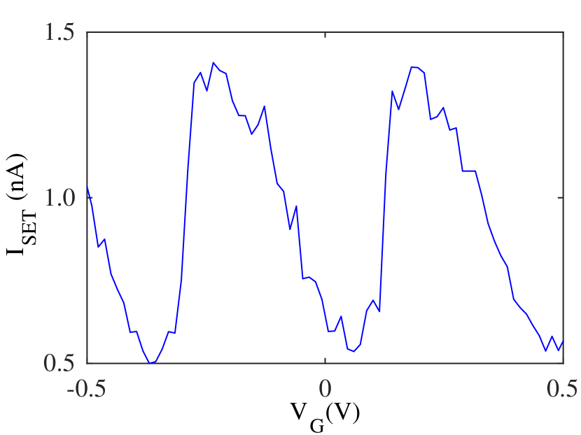
In the quartz vibration measurements with sample A, we use the optimal biasing point around the gap edge, which maximizes the modulation of by , marked by an arrow in Fig. 2(a). Figure 2(c) displays the gate dependence of the current around such optimal biasing, showing approximately sinusoidal dependence with a peak-to-peak amplitude of . Here and throughout the paper we refer to the gate voltage as the value at the room temperature generator, preceding the cryogenic voltage division.
3.1 DC readout with the SET
We begin with a simple rectification approach where in Eq. (6), allowing to measure large-amplitude vibrations. Equation (5) becomes
| (7) |
where is the zeroth order Bessel function of the first kind.
Now we excite the mechanical vibrations with voltage, thereby creating non-zero . Physically, the piezoelectric charge modulates the SET current by changing the potential of the island, in the same way as the gate voltage. In Fig. 3(a) we display such a measurement for different values of . The mechanical resonance can be observed at , as a sharp feature that depends on the gate bias. Looking at Eq. (7), the data qualitatively matches the prediction. At the current minima or maxima, where , the peak is roughly the maximum in amplitude, but disappears at the intermediate values when . Also, the sign of the peak changes according to the prediction.
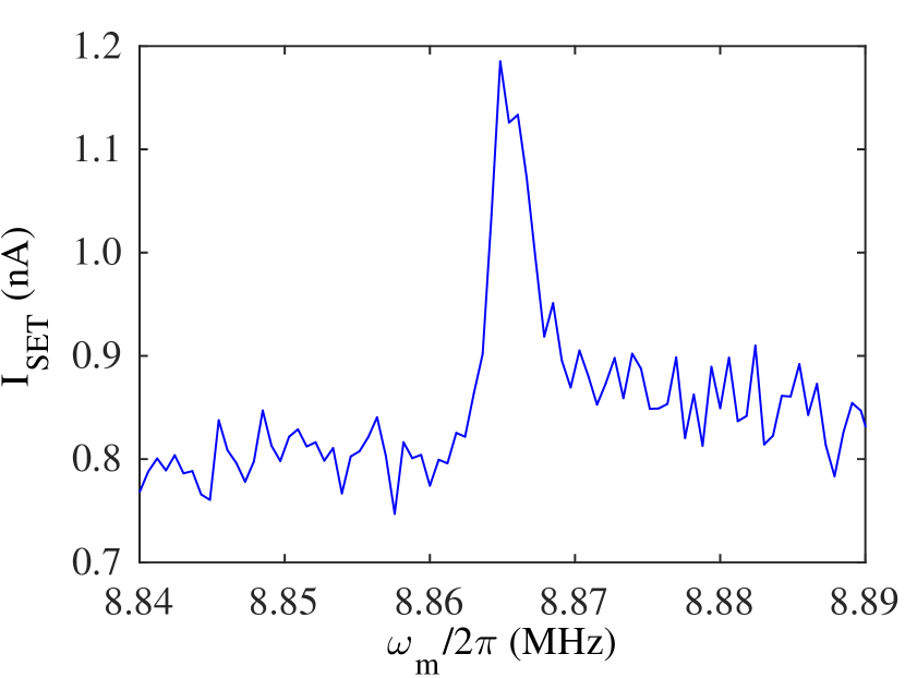
In Fig. 3(b) we display an example of a resonance peak measured at a rather large mechanical excitation voltage of , corresponding to a displacement around calculated from Eq. (2). At higher mechanical excitation amplitudes the SET current, however, starts to decrease as seen in Fig. 3(c) at where the driven charge covers more than one gate period. We can make an independent estimate of the cross-over voltage by the fact that it corresponds to the first minimum of , at , and using Eqs. (2,4) yielding , in a good agreement with the measurement.
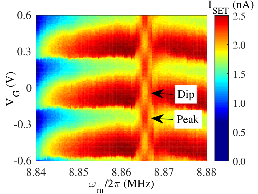
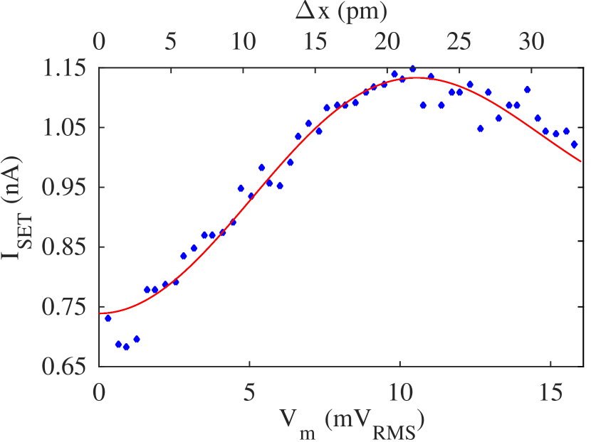
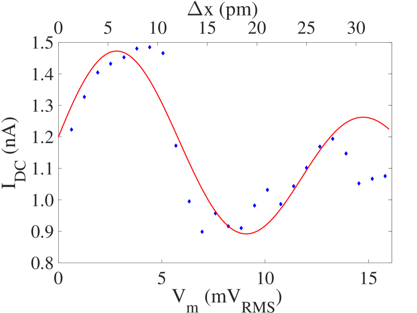
The lowest mechanical excitation amplitude with which we could still use the DC rectification method to discern the mechanical resonance peak with this setup is that corresponds to and . The linewidth of the mechanical peak is Hz, corresponding to a mechanical Q value of . That Q value is modest compared to what is in principle achievable with quartz resonators goryachev2012 . We expect this is due to the fact that the disk was fully flat in cross section profile, which does not result in confinement of the mechanical vibration in the disk center, and hence there can be pronounced energy leakage through the supports.
3.2 Homodyne and heterodyne mixing schemes
Although the DC rectification is a simple and robust method to obtain the signal at large excitation amplitudes, its sensitivity vanishes towards small vibrations. An improved approach is to use the SET as an RF mixer knobel81 in the setups shown in Figs. 1b,c. Mixer operation entails that a strong local oscillator (LO) at the frequency , see Eq. (6), is applied to the SET gate, while the actuation tone goes to the actuation electrode as above. In homodyne detection, the LO frequency is the same as the mechanical excitation frequency, , and the signal appears as a DC offset similar to the rectification setup. The device has the same bandwidth as the standard SET, but with a tunable measurement center frequency. The DC biasing is done in a fashion similar to that described in the previous section. In terms of complexity, the homodyne setup is comparable to the rectification setup. Analogous to Eq. (7) we obtain the homodyne current
| (8) |
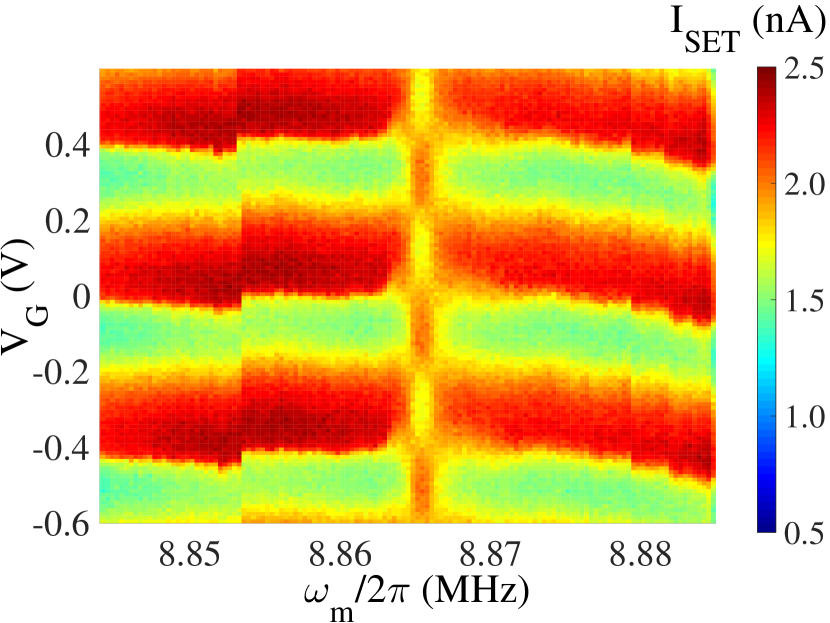
which allows for linear detection at small amplitudes. Here, is the first-order Bessel function of the first kind. In Fig. 4(a) we see, similar to Fig. 3(a), the mechanical mode at . In Fig. 4(b) we show the SET current caused by the increase of the mechanical vibration amplitude when the mechanics is actuated on-resonance. The increased sensitivity of the homodyne detection over the DC method enables the visibility of the mechanical resonance peak at smaller mechanical excitation voltages down to . That corresponds to and . The theoretical curve plotted in Fig. 4(b), calculated from Eq. (8), matches well the homodyne experimental data.
Direct conversion to DC, either using the DC method or homodyne detection, encompasses challenges, namely DC offsets from self-mixing of the excitation signal, and in particular, charge noise that is dominant in charge-sensitive devices at low frequencies. In heterodyne detection, the gate electrode is excited by a local oscillator with frequency different from the mechanical excitation frequency . The response of the SET current is then mixed down to an intermediate frequency (IF) equal to . The relevant current is given as
| (9) |
The intermediate frequency needs to be within the bandwidth of the SET setup. Here, we used kHz. In the heterodyne setup shown in Fig. 1c, the SET current is detected by a current pre-amplifier, then acquired by a DAQ board and processed in the frequency domain. Here, we used a different sample B, although the setup is expected to work also with the sample A used for the other measurements discussed. Figure 5(a) shows the IV curve of the SET in sample B. We operate at the Josephson Quasiparticle (JQP) peak, originated from the tunnelling of Cooper pairs through one junction followed by two successive quasiparticle tunneling events through the other junction. Instead of the quasiparticle current onset (Fig. 2(a)) used in the measurements discussed above, in this sample we found the JQP peak biasing provides a strong gate modulation as shown in Fig. 5(b). We relate this to the lower resistance of sample B, providing pronounced Cooper pair tunneling features.
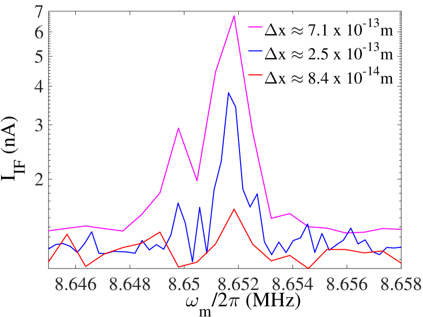
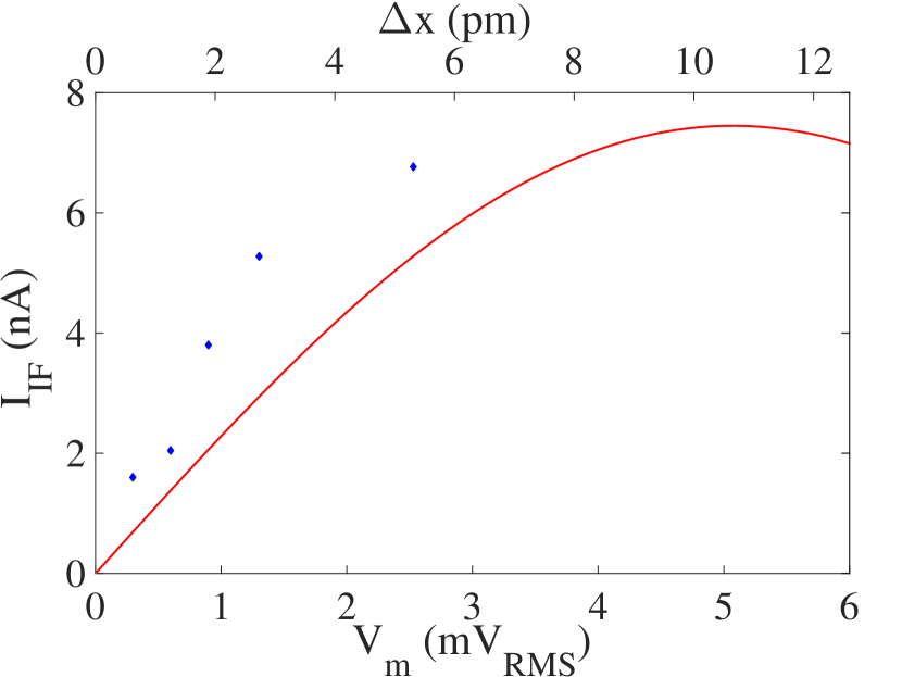
Figure 6(a) displays the detected mechanical signal, with the local oscillator amplitude roughly optimized. Comparing to Fig. 4(a) it is clear that the heterodyne scheme disposes of the DC response of the SET, hence making the data easier to interpret. Figure 6(b) shows the mechanical resonance peaks for different mechanical excitation amplitudes. The elimination of low-frequency noise by the heterodyne setup allows to measure the mechanical vibrations down to . This is an improvement over the homodyne setup, although since the data were obtained from different samples, the origin of the improvement is not necessarily in the mixing scheme used. The dependence of with the mechanical excitation amplitude is presented in Fig. 6(c). The solid line represents a theory curve calculated from Eq. (9) with obtained from Fig. 5(b) and . The data points follow the shape of the theoretical curve, however, display double the amplitude as predicted by independent estimates, a fact we attribute to inaccuracies in the local oscillator amplitude.
3.3 Radio-frequency SET as a displacement sensor
In the RF-SET setup Schoelkopf1238 ; blencowe2000 , the SET is impedance-matched to 50 microwave cables via an LC tank resonator circuit. The inductor and capacitor at the input of the SET, see Fig. 1d, form the tank circuit with resonance frequency , loaded by the SET.
When the SET resistance changes, due to piezo vibrations as here, the loading of the LC circuit by the SET changes, hence modulating the reflected power of a monochromatic carrier wave sent down the input line. The carrier appears as a time-dependent voltage across the SET, with the amplitude . The SET conductance is
| (10) |
The information is the power of the sidebands that appear at frequencies offset by the actuation frequency from a carrier applied at , obtained by detecting the carrier at room temperature. Under , the first sideband amplitude is
| (11) |
The transmitted and reflected waves are separated by circulators at base temperature stage of the refrigerator, so the reflected power can be measured by a spectrum analyzer. The bias-T allows for DC biasing the SET, needed to obtain a charge-sensitive response.
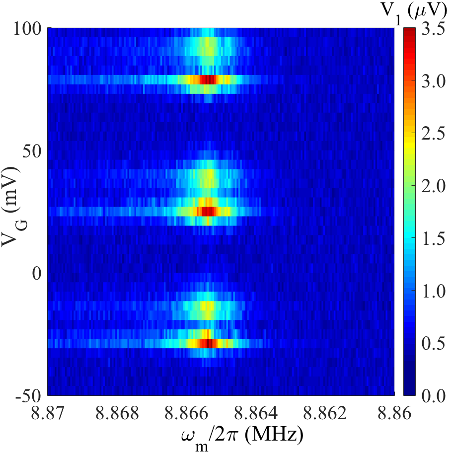
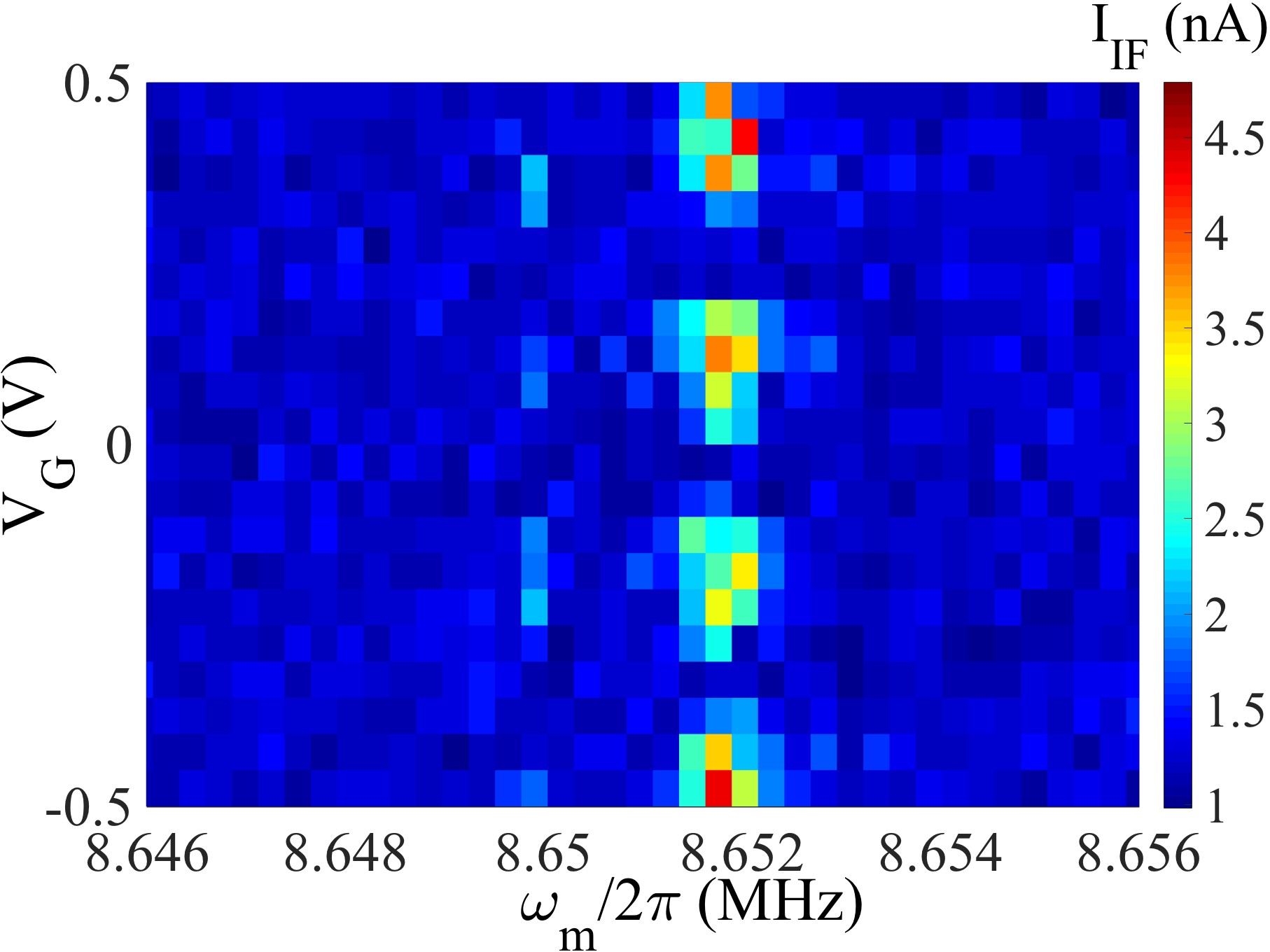
In the present system the tank circuit capacitance and inductance come from the bonding wires’ and bonding pad’s stray inductance and capacitance, respectively. The sample box configuration and bonding wires lengths and placements were simulated with Sonnet software and tweaked to set the tank circuit resonance frequency around . As an example, Fig. 7(a) shows a RF-SET measurement displaying the mechanical peak. For the following measurements, the gate and SET bias voltages were chosen so that the maximum SET differential resistance modulation is obtained.
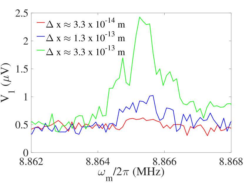
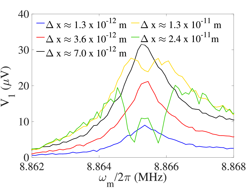
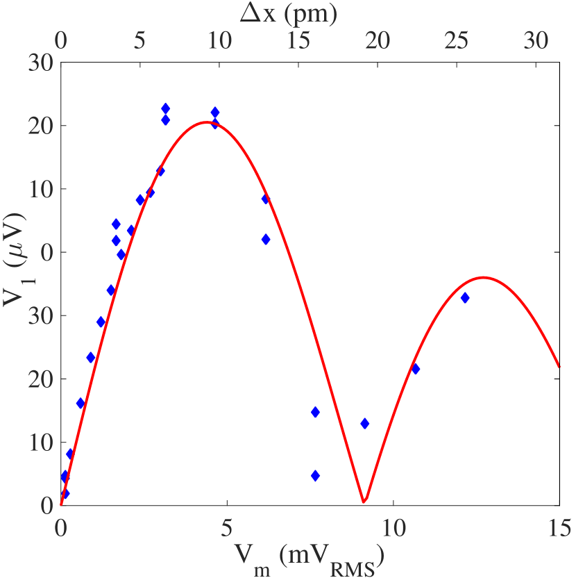
Figs. 7(b),c present examples of the mechanical resonance curves. Each curve represents the amplitude of the sideband of the carrier. Similar to the other detection methods discussed above, we can enter the nonlinear regime of the SET response, that is, observe the full Bessel dependence in Eq. (11). Splitting of the peaks is due to the fact that the driven charge at on-resonance drive is larger than at off-resonant drive. The lowest mechanical excitation amplitude with which we could still discern the mechanical resonance peak with this setup is , which corresponds to m, more than 20 times better than the other techniques.
4 Conclusions
We have shown that single electron transistor (SET) is a viable tool to detect minuscule mechanical vibrations in millimetre sized monolithic quartz disk resonators. We compared four detection schemes; DC rectification, homodyne and heterodyne mixing detection, and an approach based on the radio-frequency SET. We found that over the compared schemes, RF-SET is superior in sensitivity over mixing methods, allowing to measure oscillations down to m within the mechanical linewidth, corresponding to the sensitivity m. The zero-point motion of our quartz disk resonators is of the order of , hence it is still beyond the capabilities of our SET based detectors.
The performance can be improved, first of all, by increasing the sensitivity of the rf-SET to the piezo charge. In the current setup, the charge sensitivity is around that leaves plenty of room for improvement up to the best demonstrated values Delsing2006 . This entails in particular designing an on-chip tank circuit having a high Q value, and also increasing the charging energy by fabricating smaller junctions.
Another limiting factor is that the piezoelectric surface charge originating from the mechanical strain gets spread across a diameter circular area; while our SET sensitive area, the island, is just . This limits the charge coupled to the island to a very small fraction of the total piezoelectric charge generated by a given deformation of the quartz disk. At the moment the amount of charge coupled to the island due to is of the order . One could increase the island size in order to boost up the coupled charge. However this would lead to an increase in the island capacitance, decreasing the Coulomb gap and possibly reducing the detector sensitivity. Thus the island size is a trade-off between the SET sensitivity and the charge it couples to. We note, however, that since quartz has a low dielectric constant , the charging energy is currently set by the junctions.
The most important challenge to tackle is to increase the mechanical Q value, allowing to narrow down the detection bandwidth. With high Q values demonstrated by monolithic quartz resonators, combined with the best charge sensitivities mentioned above, and possibly with low-noise Josephson parametric amplifiers to further reduce the detection noise Siddiqi2015Amp , one would reach the level of sensitivity needed to observe vibrations at the single-quantum level with the current amount of coupled charge. Plano-convex cross-section profile onoe2005 of the quartz disks would focus the mode energy in the center, hence mitigating anchor losses that we believe are limiting the losses.
The work paves the way towards studying massive mechanical resonators near the quantum limit of their motion. Monolithic quartz resonators are suitable for this purpose since they are tangible, sturdy, durable and easily manipulated objects in contrast with other micrometer sized resonators, and can have high quality factors at frequencies of tens of MHz. They can be easily integrated in other devices without the need of advanced fabrication techniques. The millimetre-size diameter of the disk resonators provides a large sensing area that can be coupled to other macroscopic object to sense mechanical loadings. It can excel at applications that require a simple design that can measure very small strains over a large sensing area.
Acknowledgements.
This work was supported by the Academy of Finland (contract 250280, CoE LTQ, 275245), the European Research Council (615755-CAVITYQPD), the Centre for Quantum Engineering at Aalto University, and by the Finnish Cultural Foundation (Central Fund 00160903). The work benefited from the facilities at the OtaNano - Micronova Nanofabrication Center and at the Low Temperature Laboratory.References
- (1) J.A. Sidles, J.L. Garbini, K.J. Bruland, D. Rugar, O. Züger, S. Hoen, C.S. Yannoni, Rev. Mod. Phys. 67, 249 (1995). URL https://link.aps.org/doi/10.1103/RevModPhys.67.249
- (2) T.A. Palomaki, J.D. Teufel, R.W. Simmonds, K.W. Lehnert, Science 342(6159), 710 (2013). DOI 10.1126/science.1244563. URL http://science.sciencemag.org/content/342/6159/710
- (3) E.E. Wollman, C.U. Lei, A.J. Weinstein, J. Suh, A. Kronwald, F. Marquardt, A.A. Clerk, K.C. Schwab, Science 349(6251), 952 (2015). DOI 10.1126/science.aac5138. URL http://science.sciencemag.org/content/349/6251/952
- (4) J.M. Pirkkalainen, E. Damskägg, M. Brandt, F. Massel, M.A. Sillanpää, Phys. Rev. Lett. 115, 243601 (2015). URL https://link.aps.org/doi/10.1103/PhysRevLett.115.243601
- (5) F. Lecocq, J.B. Clark, R.W. Simmonds, J. Aumentado, J.D. Teufel, Phys. Rev. X 5, 041037 (2015). URL https://link.aps.org/doi/10.1103/PhysRevX.5.041037
- (6) A.N. Cleland, M.L. Roukes, Appl. Phys. Lett. 69(18), 2653 (1996). URL http://dx.doi.org/10.1063/1.117548
- (7) A. Cleland, M. Roukes, Sensors and Actuators A: Physical 72(3), 256 (1999)
- (8) P. Mohanty, D.A. Harrington, M.L. Roukes, Physica B: Condensed Matter 284-288, 2143 (2000). URL http://www.sciencedirect.com/science/article/pii/S092145269902997X
- (9) T.F. Li, Y.A. Pashkin, O. Astafiev, Y. Nakamura, J.S. Tsai, H. Im, Appl. Phys. Lett. 92, 043112 (2008)
- (10) D.W. Carr, S. Evoy, L. Sekaric, H.G. Craighead, J.M. Parpia, Applied Physics Letters 75(7), 920 (1999). URL http://dx.doi.org/10.1063/1.124554
- (11) H. Kim, D.H. Shin, K. McAllister, M. Seo, S. Lee, I.S. Kang, B.H. Park, E.E.B. Campbell, S.W. Lee, ACS Applied Materials & Interfaces 9(8), 7282 (2017). URL http://dx.doi.org/10.1021/acsami.6b16278
- (12) G.A. Steele, A.K. Hüttel, B. Witkamp, M. Poot, H.B. Meerwaldt, L.P. Kouwenhoven, H.S.J. van der Zant, Science 325(5944), 1103 (2009). URL http://science.sciencemag.org/content/325/5944/1103
- (13) B. Lassagne, Y. Tarakanov, J. Kinaret, D. Garcia-Sanchez, A. Bachtold, Science 325(5944), 1107 (2009). URL http://science.sciencemag.org/content/325/5944/1107
- (14) P.F. Cohadon, A. Heidmann, M. Pinard, Phys. Rev. Lett. 83, 3174 (1999)
- (15) S. Gigan, H.R. Bø”hm, M. Paternostro, F. Blaser, G. Langer, J.B. Hertzberg, K.C. Schwab, D. B\a”uerle, M. Aspelmeyer, A. Zeilinger, Nature 444, 67 (2006)
- (16) O. Arcizet, P.F. Cohadon, T. Briant, M. Pinard, A. Heidmann, Nature 444, 71 (2006)
- (17) C.A. Regal, J.D. Teufel, K.W. Lehnert, Nature Physics 4, 555 (2008)
- (18) D.J. Flees, S. Han, J.E. Lukens, Phys. Rev. Lett. 78, 4817 (1997). URL https://link.aps.org/doi/10.1103/PhysRevLett.78.4817
- (19) P. Joyez, P. Lafarge, A. Filipe, D. Esteve, M.H. Devoret, Phys. Rev. Lett. 72, 2458 (1994). URL https://link.aps.org/doi/10.1103/PhysRevLett.72.2458
- (20) R.G. Knobel, A.N. Cleland, Nature 424(6946), 291 (2003). URL http://dx.doi.org/10.1038/nature01773
- (21) M.D. LaHaye, O. Buu, B. Camarota, K.C. Schwab, Science 304(5667), 74 (2004). DOI 10.1126/science.1094419. URL http://science.sciencemag.org/content/304/5667/74
- (22) Y.A. Pashkin, T.F. Li, J.P. Pekola, O. Astafiev, D.A. Knyazev, F. Hoehne, H. Im, Y. Nakamura, J.S. Tsai, Appl. Phys. Lett. 96(26), 263513 (2010). URL http://dx.doi.org/10.1063/1.3455880
- (23) M.D. LaHaye, J. Suh, P.M. Echternach, K.C. Schwab, M.L. Roukes, Nature 459, 960 (2009)
- (24) A.D. O’Connell, M. Hofheinz, M. Ansmann, R.C. Bialczak, M. Lenander, E. Lucero, M. Neeley, D. Sank, H. Wang, M. Weides, J. Wenner, J.M. Martinis, A.N. Cleland, Nature 464, 697 (2010)
- (25) J.M. Pirkkalainen, S.U. Cho, J. Li, G.S. Paraoanu, P.J. Hakonen, M.A. Sillanpää, Nature 494, 211 (2013)
- (26) J.M. Pirkkalainen, S.U. Cho, F. Massel, J. Tuorila, T.T. Heikkila, P.J. Hakonen, M.A. Sillanpää, Nature Communications 6, 6981 (2015)
- (27) M.V. Gustafsson, T. Aref, A.F. Kockum, M.K. Ekström, G. Johansson, P. Delsing, Science 346, 207 (2014)
- (28) F. Rouxinol, Y. Hao, F. Brito, A.O. Caldeira, E.K. Irish, M.D. LaHaye, Nanotechnology 27(36), 364003 (2016). URL http://stacks.iop.org/0957-4484/27/i=36/a=364003
- (29) J.T. Santos, J. Li, J. Ilves, C.F. Ockeloen-Korppi, M. Sillanpää, New Journal of Physics 19(10), 103014 (2017). URL http://stacks.iop.org/1367-2630/19/i=10/a=103014
- (30) M. Woolley, M. Emzir, G. Milburn, M. Jerger, M. Goryachev, M. Tobar, A. Fedorov, Phys. Rev. B 93, 224518 (2016)
- (31) R. Knobel, A.N. Cleland, Appl. Phys. Lett. 81(12), 2258 (2002). URL http://dx.doi.org/10.1063/1.1507616
- (32) J.A. Sidles, Appl. Phys. Lett. 58(24), 2854 (1991). URL https://doi.org/10.1063/1.104757
- (33) J. Pettersson, P. Wahlgren, P. Delsing, D.B. Haviland, T. Claeson, N. Rorsman, H. Zirath, Phys. Rev. B 53, R13272 (1996). URL https://link.aps.org/doi/10.1103/PhysRevB.53.R13272
- (34) E.H. Visscher, J. Lindeman, S.M. Verbrugh, P. Hadley, J.E. Mooij, W. van der Vleuten, Appl. Phys. Lett. 68(14), 2014 (1996). URL http://dx.doi.org/10.1063/1.115622
- (35) R. Knobel, C.S. Yung, A.N. Cleland, Appl. Phys. Lett. 81(3), 532 (2002). URL http://dx.doi.org/10.1063/1.1493221
- (36) M.T. Abuelma’atti, Analog Integrated Circuits and Signal Processing 61(3), 223 (2009). URL https://doi.org/10.1007/s10470-009-9304-z
- (37) R.J. Schoelkopf, P. Wahlgren, A.A. Kozhevnikov, P. Delsing, D.E. Prober, Science 280(5367), 1238 (1998). URL http://science.sciencemag.org/content/280/5367/1238
- (38) M.H. Devoret, R.J. Schoelkopf, Nature 406(6799), 1039 (2000). URL http://dx.doi.org/10.1038/35023253
- (39) M. Goryachev, D.L. Creedon, E.N. Ivanov, S. Galliou, R. Bourquin, M.E. Tobar, Appl. Phys. Lett. 100(24), 243504 (2012)
- (40) M. Blencowe, M. Wybourne, Appl. Phys. Lett. 77, 3845 (2000)
- (41) H. Brenning, S. Kafanov, T. Duty, S. Kubatkin, P. Delsing, J. Appl. Phys. 100(11), 114321 (2006). URL http://aip.scitation.org/doi/abs/10.1063/1.2388134
- (42) C. Macklin, K. O Brien, D. Hover, M.E. Schwartz, V. Bolkhovsky, X. Zhang, W.D. Oliver, I. Siddiqi, Science 350, 307 (2015)
- (43) M. Onoe, in Proceedings of the 2005 IEEE International Frequency Control Symposium and Exposition, 2005. (IEEE, 2005), pp. 433–441