Hot electron cooling in Dirac semimetal Cd3As2 due to polar optical phonons
Abstract
A theory of hot electron cooling power due to polar optical phonons is developed in three-dimensional Dirac semimetal(DDS) Cd3As2 taking account of hot phonon effect. Hot phonon distribution and are investigated as a function of electron temperature , electron density , and phonon relaxation time . It is found that increases rapidly (slowly) with at lower (higher) temperature regime. Whereas, is weakly deceasing with increasing . The results are compared with those for three-dimensional electron gas (DEG) in Cd3As2 semiconductor. Hot phonon effect is found to reduce considerably and it is stronger in 3DDS Cd3As2 than in Cd3As2 semiconductor. is also compared with the hot electron cooling power due to acoustic phonons . We find that a crossover takes place from dominated cooling at low to dominated cooling at higher . The temperature at which this crossover occurs shifts towards higher values with the increase of . Also, hot electron energy relaxation time is discussed and estimated.
pacs:
72.10.-d, 73.63.-b 73.20.-rI Introduction
Recently, theoretically predictedWang_1 ; Wang_2 and by now experimentally realized and verified three-dimensional Dirac semimetals (3DDS) have become the rapidly growing field of research interestBoris ; Liu ; Neupan ; Jeon ; L_He ; zk_Liu ; T_Liang ; YZhao ; Weber ; H_Weng ; Wang_3 ; W_Lu ; Zhu ; cp_Weber ; C_Zhu . These 3DDS, the three-dimensional (3D) analogue of graphene, have gapless band feature with linear band dispersion and vanishing effective mass in their low energy states. The cadmium arsenide ( Cd3As2), a potential representative of 3DDS, has drawn more attention as it is robust and chemically stable compound in air with ultrahigh mobilityLiu ; Neupan ; T_Liang ; YZhao . The linear band picture of 3D Dirac fermions has lead 3DDS to exhibit many unusual transport phenomena such as strong quantum oscillationsL_He ; YZhao , ultrahigh mobilityT_Liang ; YZhao ; J_Feng and giant magneto resistanceT_Liang ; J_Feng ; A_Narayan ; H_Li . Besides, several promising applications of bulk Dirac fermions in Cd3As2 in photonic devices such as ultrafast broadband infrared photodetectorsWang_3 and ultrafast optical switching mechanism for the mid-infraredC_Zhu have been realized and demonstrated. Because of the inherent zero energy gap and linear band dispersion, 3DDS can absorb photons in the entire infrared region. These DDS have advantage over two-dimensional (D) Dirac semimetals like monolayer graphene because bulk nature of DDS enhances the efficiency of photon absorption.
The experimentally reported low temperature ( K) high mobilities cm2/V-s Neupan ; Jeon ; T_Liang ; YZhao and up to cm2/V-sYZhao are higher than that in suspended graphene. The measurements of resistivity vs temperature , show down to low , which is inferred to be due to umklapp processes and electron-optical phonon scatteringYZhao . High quality DDS Cd3As2 microbeltsZG_Chen and nanobeltsE_Zhang with room temperature electron mobility cm2/V-s have been fabricated. In nanobeltE_Zhang , the Hall mobility follows the typical relation with =, in the range - K, which is attributed to the enhanced electron-phonon (el-ph) scattering.
Theoretically, electronic transport properties of D Weyl and Dirac semimetals are studied using the semi-classical Boltzmann transport equationLundgren ; SD_Sarma . Considering the electron momentum relaxation processes due to scattering by disorder (short-range and long-range) and acoustic phonons, the latter is shown to dominate electrical conductivity at higher temperatureSD_Sarma . However, the quantitative comparison between the existing experimental results and theoretical calculations is still lacking.
In order to find the applications of DDS in devices operating in the high field region, it is important to investigate the steady state energy relaxation of the hot carriers, in these systems, by emission of phonons as the only cooling channel. In high electric field electrons gain energy and establish their ‘hot electron temperature ’ which is greater than the lattice temperature . In the steady state these hot electrons transfer their energy to lattice by emission of acoustic (optical) phonons at relatively low (high) temperature. The electron heating affects the device operation significantly, in the high field region, as it governs the thermal dissipation and heat management. To enhance the device efficiency, it is important to reduce the hot electron power loss.
The hot electron energy relaxation by emission of acoustic and optical phonons has been extensively investigated theoretically and experimentally in conventional D electron gas (DEG) in bulk semiconductorsConwell ; Seeger ; InSb ; GaAs ; SD_Sarma2 ; Prabhu ; Ridley_1 , D electron gas (2DEG) in semiconductor heterostructuresRidley_1 ; Price , monolayer grapheneSSK and bilayer grapheneSSK_B . Recently, hot electron cooling is theoretically studied in monolayer MoS2Kaasbjrg and quasi-2DEG in gapped Cd3As2 filmCd_Film . There exist theoretical studies of hot D Dirac fermion cooling power due to electron-acoustic phonon interaction in Cd3As2Lundgren_2 ; KS_Bhargv . The deformation potential coupling constant (- eV)Jay_Gerin determines the strength of electron-acoustic phonon scattering. In the Bloch-Grüneisen (BG) regime the power laws of dependence on electron temperature and electron density are predictedKS_Bhargv .
Experimentally, the phonon mediated hot electron cooling of photoexcited carriers has been investigated in Cd3As2 from pump-probe measurementsWeber ; W_Lu ; Zhu ; cp_Weber . The cooling process of photoexcited carriers is shown to be through emission of acoustic and optical phononsWeber ; W_Lu , with relatively low optical phonon energies meVW_Lu ; Weszka . The hot electron cooling, apart from relating el-ph scattering to the high field transport properties, it also plays significant role in designing high speed electronic and photonic devices of Cd3As2. Thus, el-ph interaction is a key issue and central to the understanding of devices based on Cd3As2.
It is important to notice that, in DDS Cd3As2, although there is strong experimental evidence of photoexcited hot carrier energy relaxation by optical phonon emissionWeber ; W_Lu ; Zhu , the steady state hot electron cooling by emission of optical phonons has not been addressed both theoretically and experimentally. In the present work, we theoretically investigate the hot electron cooling power in DDS Cd3As2 by emission of optical phonons including the hot phonon effect. Numerical results are obtained as a function of electron temperature, electron density and phonon relaxation time. These results are compared with in bulk Cd3As2 semiconductor and with , in DDS Cd3As2. This study is expected to provide thermal link between electrons and phonons in DDS Cd3As2 for its application in high speed/field devices.
The structure of the paper is shaped in the following way. In section II we provide all the theoretical ingredients including hot phonon effect, cooling power due to optical and acoustic phonons in DDS Cd3As2, and cooling power for DEG in bulk Cd3As2 semiconductor. The obtained results are discussed in section III. Finally a summary of the present work is given in section IV.
II Theory
In this section we develop a theory for the cooling power of hot electrons in DDS mediated by polar optical phonons. For comparison purpose we shall also provide the results for cooling power due to acoustic phonon in DDS as well as that in bulk Cd3As2 semiconductor due to polar optical phonon. Let us start with mentioning the basic properties of the physical system chosen.
II.1 Preliminary informations
We consider the Dirac fermion gas in a DDS Cd3As2 in which the low energy excitations are described by the Dirac like linear dispersion in the long wavelength continuum limit. Here, is the Fermi velocity, is the D electronic wave vector, and the band index takes the value for conduction(valence) band. The corresponding eigenstate is given by , where is the volume of the system, and with and are the polar and azimuthal angle in three dimensional -space, respectively. The corresponding density of states is given by , where with is the spin(valley) degeneracy.
II.2 Hot electron cooling power in DDS
In order to formulate a theory for the hot electron cooling power in 3DDS, we work in the “hot electron temperature model” in which the electron gas is assumed to be in equilibrium with itself at an elevated temperature than the lattice temperature . In this model Dirac fermions are assumed to have the usual Fermi-Dirac distribution where and is the chemical potential determined by the electron density . The 3D Dirac fermions are assumed to interact with the D phonons of energy and wave vector . The cooling power per electron (i.e. average electron energy loss rate) due to el-ph interaction can be obtained by using the well known technique described in Ref. [Conwell, ]. It is given by
| (1) |
where is total number of electrons, is the non-equilibrium phonon distribution function. The rate of change of due to electron-phonon interaction i.e. is given by using Fermi’s golden rule
| (2) | |||||
where is the square of the matrix element for the el-ph interaction. Here, is square of el-ph matrix element without chiral wave function and with being the angle between and , resulting from the chiral nature of the Dirac fermion.
As a result the cooling power(Eq. (1)) becomes
| (5) |
Our objective is to find hot electron cooling power due to optical phonons. The optical phonon energy is taken to be constant. The summation over in Eq. (5) can be converted into integral as with and are the polar and azimuthal angle of , respectively. Note that the integrations over and give . Defining , we find hot electron cooling power as
| (6) |
An explicit evaluation of is given in the section II(D).
II.3 Hot phonon distribution
Non-equilibrium phonon distribution can be obtained from the Boltzmann equation
| (7) |
where the first term describes the rate of change of the phonon distribution due to electron-phonon interaction while the later one denotes the same due to the other processes namely phonon-phonon interaction, surface roughness scattering etc.
In the relaxation time approximation one can write
| (8) |
where, with is the phonon distribution at equilibrium and is phonon relaxation time due to all other mechanisms.
Hence, the non-equilibrium phonon distribution will be readily obtained from Eq.(7) as
| (9) |
II.4 Evaluation of
Here, we shall provide an explicit evaluation of el-ph scattering rate . We assume the electron-optical phonon interaction via Fröhlich coupling with the corresponding matrix element , where is the high frequency (static) dielectric constant of the material. Momentum conservation also allow us to write as
| (11) |
Converting the summation over into integrals like , Eq.(4) becomes
| (12) | |||||
where the argument of the delta function is
| (13) |
with . Note that the -integral in Eq. (12) gives since the integrand is independent of . The -integral can be evaluated by the following property of the delta function
| (14) |
where the root of Eq.(13) can be obtained as
| (15) |
Hence, after doing the angular integrations, Eq. (12) becomes
| (16) | |||||
where . This lower limit of -integral is a consequence of the fact that . Note also that
| (17) |
II.5 Hot electron cooling power due to acoustic phonons in DDS
As we are giving results for hot electron cooling power due to acoustic phonons, for the sake of comparison with , the corresponding expression is given byKS_Bhargv
| (18) | |||||
where is the acoustic phonon deformation potential coupling constant, is the acoustic phonon velocity, is the mass density, =, =, and . The temperature dependent screening function is given by , where is the finite temperature static polarizability, evaluated explicitly in Ref.[SD_Sarma, ].
II.6 Hot electron cooling power due to optical phonons in D semiconductor
With a view to compare the results of the DDS Cd3As2 with those in D Cd3As2 semiconductor, we give the expression for the for a 3DEG in bulk Cd3As2 semiconductor. Taking the parabolic energy relation ( is the effective mass of electron), it is given by
| (19) | |||||
In this case . The corresponding el-ph scattering rate is given by
| (20) |
where .
II.7 Electron energy relaxation time
Some times it is useful to study the hot electron relaxation in terms of corresponding relaxation time , given byRidley_3 where is the average energy of the electron at temperature . For large electron density and very low temperature, expressing density of states , we find
| (21) |
where is the Fermi energy at =. This formula is applicable to D and D fermions and Dirac fermions with the respective choice of and .
III Results and Discussions
In the following, we numerically study the hot phonon distribution and electron cooling power in D Dirac semimetal Cd3As2 in the range for electron temperature =- K and electron density =-, where = m-3, taking the lattice temperature = K. In addition, we present some results of acoustic phonon limited hot electron cooling power in Cd3As2. For comparison we also highlight on the electron cooling power in conventional 3DEG. The values of the parameters appropriate for numerical calculations are given in Table I.
| Parameter | Symbol | Value |
|---|---|---|
| Lattice constant | 4.6 Angstrom | |
| Effective mass of electronJay_Gerin | ||
| Mass density of ion | Kg/m3 | |
| Degeneracy | ||
| For 3DDS | g | 4 |
| For 3DEG | g | 2 |
| Sound velocity | m/s | |
| Fermi velocityLundgren_2 | m/s | |
| Deformation potentialJay_Gerin | 20 eV | |
| Optical phonon energyW_Lu ; Weszka | meV | |
| Dielectric constant(High Freq.) | 12 | |
| Dielectric constant(Static) | 36 | |
| Electron density | - | |
| Lattice temperature | K | |
| Electron temperature | -K |
Hot phonon distribution as a function of is shown for different , , and , respectively, in Fig. 1 for DDS Cd3As2. In all the three figures we notice that varies considerably and this dependence is determined by arising from the electron-optical phonon interaction in Eq.(16). Each curve has a broad maximum for about = m-1 where the phonon heating is found to be significant. This corresponds to the phase matching phonon wave vector = m-1 given by . The initial steep increase of may be attributed to the lower limit of integration in the Eq.(16). After a broad maximum, with further increase of , the is found to decrease first very slowly and then gradually to zero. Similar observations are made in GaAs heterojunctionsZJ_Zhang2 , bilayer grapheneKatti and monolayer MoS2Kaasbjrg . Writing as the hot phonon number given by Bose distribution at an effective hot phonon temperature , it can be shown from Eq. (10) that, for , , and the approaches the .
In Fig. 1(a), vs is shown for different =, , , and K with = and = ps. The phonon number increases with increasing , as expected on the physical ground that electrons with larger can emit large number of phonons. The corresponding to = K is very small compared to the other values, with largest value of corresponding to K. The width of the maximum is larger for smaller , similar to the findings in monolayer MoS2Kaasbjrg .
dependence on phonon relaxation time is shown in Fig. 1(b) by plotting vs for = , , , and ps with = and = K. Number of hot phonons is found to be larger for larger relaxation time, as anticipated. Secondly, we notice that the range of for which remains maximum and nearly constant (i.e. width of the maximum) is larger for phonons with larger .
The effect of on hot phonon distribution is shown in Fig. 1(c) for = ps at = K. The electron density chosen are =, , , and . is found to be larger for larger because larger density of electrons emit large number of phonons. Moreover, width of the maximum is larger for larger . Similar observation is made in GaN/AlGaN heterostructureGokden .
For comparison we have shown vs , in Fig. 2 for different , , and for DEG in bulk Cd3As2 semiconductor. We see that maximum of in this semiconductor is almost same as found for DDS Cd3As2 for each of the . But, unlike in DDS Cd3As2, this maximum is spread over relatively a small range of . The maximum occurs around m-1 which is closer to the phase matching value of = m-1. In the low region increases rapidly with , and after reaching the maximum it gradually decreases. Finally it vanishes at relatively larger values as compared to 3DDS. From Fig. 2(c), in which is shown for different , we see that, for Cd3As2 semiconductor remains same, unlike the case of DDS Cd3As2 ( Fig. 1c), for certain range of for all . Beyond this, is found to be larger for larger at larger .
In Fig. 3(a), we have shown electron cooling power , due to optical phonons, as a function of for different phonon relaxation time =, , , and ps. The curve for ps corresponds to without hot phonon effect. In low (about K), all the curves show rapid increase of with . This is expected because in low region is large and it decreases significantly with increase of . Consequently the optical phonon emission increases as . In the higher region, increases slowly. This behavior may be approximately put as attributing to the exponential growth of occupation of electron states with high enough energy to emit optical phonons. At = K, the is nearly and is nearly constant.
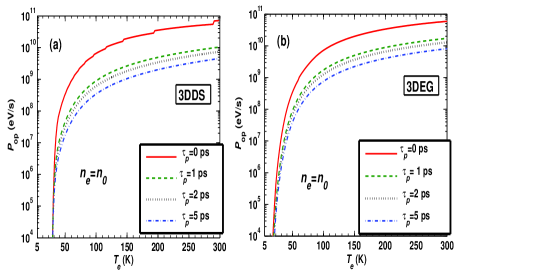
We find that the hot phonon effect reduces significantly. However, the hot phonon effect is larger for ps and smaller for higher values of . We can introduce a reduction factor = (without hot phonon effect)/(with hot phonon effect), which is always expected to be greater than . The reduction factor increases with increasing , as expected, because there is increased number of hot phonons for larger which are partially reabsorbed and hence reducing the further electron power loss. For example, for = ps, at = and K, the reduction factors are = and , respectively. For = ps, at = and K, the reduction factors, respectively, are = and . This observation indicates that hot phonon effect is sensitive at low and less sensitive at higher .
For comparison, is shown as a function of , in Fig. 3(b), for 3DEG in Cd3As2 semiconductor for = , , , and ps. It is found that without hot phonon effect (i.e =), in DEG is much larger than that in DDS in the temperature regime K. Above K, the corresponding values of are almost same. With hot phonon effect (), in DEG is larger than in DDS over the entire range of temperature considered. The difference between the values of in DEG and DDS is huge below K. However, this difference above K is small and it is increasing with . In Cd3As2 semiconductor, we find for = ps at = K, =. For = ps, it is obtained = at = K. These values of are smaller than that found in DDS. This larger reduction of in DDS Cd3As2 indicates that, at a given , hot phonon population is more in this system compared to D Cd3As2 semiconductor. This can be seen from the more broader maximum of in the former system.
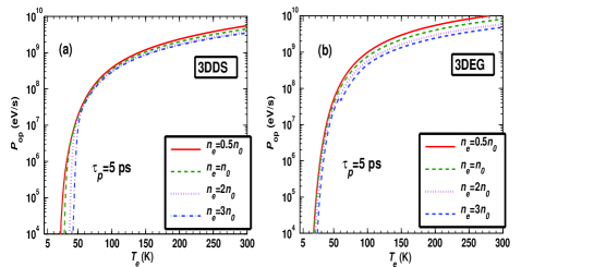
In Fig. 4(a)(4(b)) is shown as a function of for different in DDS (DEG) Cd3As2 taking =5 ps. In DDS Cd3As2 (Fig. 4(a)) is found to be smaller for larger . For about K, is found to be more sensitive to and the dependence becomes weaker at higher . However, the situation is different for DEG in Cd3As2 semiconductor. As depicted in Fig. 4(b) the sensitivity of is more in high regime than that in low range.
In Fig. 5, we show temperature dependence of hot electron cooling power due to acoustic phonons and optical phonons considering hot phonon effect (with = ps) as well as the total =. increases superlinearly in low region and then approaches , which is generic at higher . It is also found that, in this temperature range, is smaller for smaller , unlike the case of . In Fig. 5(b), we see that there is a crossover from acoustic phonon to optical phonon dominated cooling power. The at which the crossover takes place depends upon significantly. It is found that crossover takes place at , , , and K for =, , , and , respectively. Optical phonon is the active channel of power dissipation above this . The crossover temperature may depend on also. Considering =, the crossover = K may be compared with about K in InSbInSb and K in GaAsGaAs ; Prabhu bulk semiconductors noting that these samples are non-degenerate. The = K above which is dominating in Cd3As2 is closer to that in bulk InSb as optical phonon energies in these two systems are closer. It is to be noted that in InSb(GaAs) is () meV. In the neighborhood of cross over , shows a knee like behavior as found in InSbInSb and GaAsGaAs .
In the Bloch-Grüneisen (BG) regime, =(), where is the Fermi wave vector, the dependence on and are shown to be given by the power laws and where =() and =5/3(1/3) with(without) screening of electron-acoustic phonon interactionKS_Bhargv . In relatively higher () regime, disorder assisted calculations show drastic increase of cooling power due to enhanced energy transfer between electrons and acoustic phononsLundgren_2 .
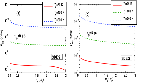
In Fig. 6(a) (6(b)) is shown as a function of for different in DDS (DEG) Cd3As2 taking = ps. In DDS Cd3As2, is found to decrease weakly with increasing . This decrease may be attributed to partial reabsorption of large number of phonons emitted by larger . The decrease is, relatively, faster(slower) at low(high) . Moreover, it is found that, compared to DEG in Cd3As2 semiconductor (Fig. 6(b)), in DDS Cd3As2 is less sensitive to . This may be attributed to differing density of states. For example, while varying from to decreases, at = K, by a factor of about in DDS (DEG) Cd3As2. At = K the respective changes are and .
Electron cooling power due to optical phonons in bulk GaAs is shown to be reduced by screening effectSD_Sarma2 . In DDS Cd3As2 also we expect the screening to reduce . Although screening effect is not considered in our calculations, the experimental measurements will be able to indicate its necessity.
We would like to mention that our numerical calculations of can be used to calculate energy relaxation time as given in section II(G). For =, the average electron energy is found to be =, , and eV at =, , and K, respectively. Consequently, taking = eV/s at = K we find energy relaxation time = ps. Alternatively, can be obtained from = , where is the electronic heat capacity. However, simple power laws can be obtained in BG regime, where is the sole contributor to electron cooling power, with regard to and dependence. Using the BG regime results, we find () and () for screened (unscreened) electron-acoustic phonon interaction.
IV Summary
In summary, we have studied optical phonon limited cooling of hot electrons in DDS Cd3As2 considering the effect of hot phonon. The dependence of electron cooling power , due to optical phonon, on electron temperature , electron density , and phonon relaxation time are investigated. is found to increase much rapidly with at low temperature regime while this increase becomes much slower in high regime. The dependence of on is weak. It shows a slow decrease with the increase of . We compare the results with those corresponding to DEG in Cd3As2 semiconductor. It is revealed that hot phonon effect is stronger in DDS Cd3As2 than in Cd3As2 semiconductor. It is also found that is more (less) sensitive to in DEG (DDS). Additionally, is compared with the acoustic phonon limited hot electron cooling power . A crossover from dominated cooling at low to dominated cooling at higher takes place at about = K for =. The crossover shifts towards higher temperature for larger . We point out that our calculations need to be tested against the experimental data. We suggest for steady state/electric field experiments in -type DDS Cd3As2 to which our present calculations will be directly related.
References
- (1) Z. Wang, Y. Sun, X. Q. Chen, C. Franchini, G. Xu, H. Weng, X. Dai, and Z. Fang, Phys. Rev. B 85, 195320 (2012).
- (2) Z. Wang, H. Weng, Q. Wu, X. Dai, and Z. Fang, Phys. Rev. B 88, 125427 (2013).
- (3) S. Borisenko, Q. Gibson, D. Evtushinsky, V. Zabolotnyy, B. Büchner, and R. J. Cava, Phys. Rev. Lett. 113, 027603 (2014).
- (4) Z. K. Liu, J. Jiang, B. Zhou, Z. J. Wang, Y. Zhang, H. M. Weng, D. Prabhakaran, S-K. Mo, H. Peng, P. Dudin, T. Kim, M. Hoesch, Z. Fang, X. Dai, Z. X. Shen, D. L. Feng, Z. Hussain, and Y. L. Chen Nat. Mater. 13, 677 (2014).
- (5) M. Neupane, S.-Y. Xu, R. Sankar, N. Alidoust, G. Bian, C. Liu, I. Belopolski, T. R. Chang, H. T. Jeng, H. Lin, A. Bansil, F. Chou, and M. Z. Hasan Nat. Commun. 5, 3786 (2014).
- (6) S. Jeon, B. B. Zhou, A. Gyenis, B. E. Feldman, I. Kimchi, A. C. Potter, Q. D. Gibson, R. J. Cava, A. Vishwanath, and A. Yazdani Nat. Mater. 13, 851 (2014).
- (7) L. P. He, X. C. Hong, J. K. Dong, J. Pan, Z. Zhang, J. Zhang, and S. Y. Li, Phys. Rev. Lett. 113, 246402 (2014).
- (8) Z. K. Liu, B. Zhou, Y. Zhang, Z. J. Wang, H. M. Weng, D. Prabhakaran, S.-K. Mo, Z. X. Shen, Z. Fang, X. Dai, Z. Hussain, and Y. L. Chen, Science 343, 864 (2014).
- (9) T. Liang, Q. Gibson, M. N. Ali, M. Liu, R. J. Cava, and N. P. Ong, Nat. Mater. 14, 280 (2015).
- (10) Y. Zhao, H. Liu, C. Zhang, H. Wang, J. Wang, Z. Lin, Y. Xing, H. Lu, J. Liu, Y. Wang, S. M. Brombosz, Z. Xiao, S. Jia, X. C. Xie, and J. Wang, Phys. Rev. X 5, 031037 (2015).
- (11) C. P. Weber, E. Arushanov, B. S. Berggren, T. Hosseini, N. Kouklin, and A. Nateprov, Appl. Phys. Lett. 106, 231904 (2015).
- (12) H. Weng, X. Dai, and Z. Fang, J. Phys. : Conds. Matt. 28, 303001 (2016).
- (13) Q. Wang, C. Z. Li, S. Ge, J. G. Li, W. Lu, J. Lai, X. Liu, J. Ma, D. P. Yu, Z. M. Liao, and D. Sun, Nano Lett. 17, 834 (2017).
- (14) W. Lu, S. Ge, X. Liu, H. Lu, C. Li, J. Lai, C. Zhao, Z. Liao, S. Jia, and D. Sun, Phys. Rev. B 95, 024303 (2017).
- (15) C. Zhu, X. Yuan, F. Xiu, C. Zhang, Y. Xu, R. Zhang, Y. Shi and F. Wang, Appl. Phys. Lett. 111, 091101 (2017).
- (16) C. P. Weber, B. S. Berggren, M. G. Masten, T. C. Ogloza, S. Deckoff-Jones, J. Madeo, M. K. L. Man, K. M. Dani, L. Zhao, G. Chen, J. Liu, Z. Mao, L. M. Schoop, B. V. Lotsch, S. S. P. Parkin, and M. Ali, J. Appl. Phys. 122, 223102 (2017).
- (17) C. Zhu, F. Wang, Y. Meng, X. Yuan, F. Xiu, H. Luo, Y. Wang, J. Li, X. Lv, L. He, Y. Xu, J. Liu, C. Zhang, Y. Shi, R. Zhang, and S. Zhu, Nat. Commun. 8, 14111 (2017).
- (18) J. Feng, Y. Pang, D. Wu, Z. Wang, H. Weng, J. Li, X. Dai, Z. Fang, Y. Shi, and L. Lu Phys. Rev. B 92, 081306 (2015).
- (19) A. Narayanan, M. D. Watson, S. F. Blake, N. Bruyant, L. Drigo, Y. L. Chen, D. Prabhakaran, B. Yan, C. Felser, T. Kong, P. C. Canfield, and A. I. Coldea Phys. Rev. Lett. 114, 117201 (2015).
- (20) H. Li, H. He, H. Z. Lu, H. Zhang, H. Liu, R. Ma, Z. Fan, S. Q. Shen, and J. Wang, Nat. Comm. 7, 10301 (2016).
- (21) Z. G. Chen, C. Zhang, Y. Zou, E. Zhang, L. Yang, M. Hong, F. Xiu, and J. Zou, Nano Lett. 15, 5830 (2015).
- (22) E. Zhang, Y. Liu, W. Wang, C. Zhang, P. Zhou, Z. Chen, J. Zou and F. Xiu, ACS Nano 9, 8843 (2015)
- (23) R. Lundgren, P. Laurell, and G. A. Fiete, Phys. Rev. B 90, 165115 (2014).
- (24) S. Das Sarma, E. H. Hwang, and H. Min, Phys. Rev. B 91, 035201 (2015).
- (25) E. M. Conwell, High field transport in semiconductors (Academic, New York, 1967).
- (26) K. Seeger, Semiconductor Physics: An Introduction, Springer Series in Solid State Sciences, 9th ed. (Springer-Verlag, Berlin Heidelberg, 2004).
- (27) J. R. Sandercock, Proc. Phys. Soc. 86, 1221 (1965); J. P. Maneval, A. Zylbersztejn, and H. F. Budd, Phys. Rev. Lett. 23 848 (1969); S. S. Kubakaddi and B. S. Krishnamurthy, Phys. Lett. A 54, 389 (1975); K. Shimomae, Y. Hirose and C. Hamaguchi, J. Phys. C: Solid State Phys., 14, 5151 (1981).
- (28) K. Hess and H. Kahlert, J. Phys. Chem. Solids 32, 2262 (1971); S. S. Kubakaddi and B. G. Mulimani, Phys. Lett. A 103, 141 (1984).
- (29) S. D. Sarma, J. K. Jain, and R. Jalabert, Phys. Rev. B 37, 6290 (1988).
- (30) S. S. Prabhu, A. S. Vengurlekar, S. K. Roy, and J. Shah, Phys. Rev. B 51, 14233 (1995).
- (31) B. K. Ridley, Rep. Prog. Phys. 54, 169 (1991).
- (32) P. J. Price, J. Appl. Phys. 53, 6863 (1982); J. Shah, A. Pinczuk, A. C. Gossard, and W. Wiegmann, Phys. Rev. Lett. 54, 2045 (1985); S. J. Manion, M. Artaki, M. A. Emanuel, J. J. Coleman and K. Hess, Phys. Rev. B 35, 9203 (1987); S. Das Sarma, J. K. Jain and R. Jalabert, Phys. Rev. B 37, 1228 (1988); Y. Ma, R. Fletcher, E. Zaremba, M. D’Iorio, C. T. Foxon, and J. J. Harris, Phys. Rev. B 43, 9033 (1991); S. S. Kubakaddi, K. Suresha, and B. G. Mulimani, Semicond. Sci. Technol. 17, 557 (2002).
- (33) S. S. Kubakaddi, Phys. Rev. B 79, 075417 (2009); R. Bistritzer and A. H. MacDonald, Phys. Rev. B 80, 085109 (2009); J. K. Viljas and T.T. Heikkila, Phys. Rev. B 81, 245404 (2010); A. C. Betz, et al., Phys. Rev.Lett. 109, 056805 (2012); J. C. W. Song, M. Y. Reizer, and L. S. Levitov, Phys. Rev. Lett. 109, 106602 (2012); A. M. R. Baker et al., Phys. Rev. B 87, 045414 (2013). R. Somphonsane, et al., Nano Lett. 13, 4305 (2013); W. Song, L.S. Levitov, J. Phys.: Condens. Matter 27, 164201(2015).
- (34) K. S. Bhargavi and S. S. Kubakaddi, Physica E 56, 123 (2014); J. Huang et al., J. Phys.: Condens. Matter 27, 164202 (2015); A. Laitinen et al., Phys. Rev. B 91, 121414(R) (2015); S. S. Kubakaddi, Physica E 95, 144 (2018).
- (35) K. Kaasbjerg, K. S. Bhargavi, and S. S. Kubakaddi, Phys. Rev. B 90, 165436 (2014).
- (36) S. Huang, M. Sanderson, J. Tian, Q. Chen, F. Wang, and C. Zhang, J. Phys. D: Appl. Phys. 51, 015101 (2018).
- (37) R. Lundgren and G. A. Fiete, Phys. Rev. B 92, 125139 (2015).
- (38) K. S. Bhargavi and S. S. Kubakaddi, Phys. Staus Solidi RRL 10, 248 (2016). \textcolorblueIn this paper a typo error to be deleted in the denominator of r.h.s of Eq.(1)
- (39) J. P. Jay-Gerin, M. J. Aubin and L. G. Caron, Phys. Rev. B 18, 4542 (1978).
- (40) J. Weszka, Phys. Stat. Sol. (b) 211, 605 (1999).
- (41) B. K. Ridley, Quantum Processes in Semiconductors, 2nd edition, Oxford science Publications,( Clarendon Press, Oxford, 1988), p. 327.
- (42) J. Z. Zhang, B. F. Zhu, and J. Huang, Phys. Rev. B 59, 13184 (1999).
- (43) V. S. Katti and S. S. Kubakaddi, J. Appl. Phys. 113, 063705 (2013).
- (44) S. Gokden, N. Balkan, and B. K. Ridley, Semicond. Sci. Technol. 18, 206 (2003).