Singlet and triplet trions in WS2 monolayer encapsulated in hexagonal boron nitride
Abstract
Embedding a WS2 monolayer in flakes of hexagonal boron nitride allowed us to resolve and study the photoluminescence response due to both singlet and triplet states of negatively charged excitons (trions) in this atomically thin semiconductor. The energy separation between the singlet and triplet states has been found to be relatively small reflecting rather weak effects of the electron-electron exchange interaction for the trion triplet in a WS2 monolayer, which involves two electrons with the same spin but from different valleys. Polarization-resolved experiments demonstrate that the helicity of the excitation light is better preserved in the emission spectrum of the triplet trion than in that of the singlet trion. Finally, the singlet (intravalley) trions are found to be observable even at ambient conditions whereas the emission due to the triplet (intervalley) trions is only efficient at low temperatures.
-
May 2018
1 Introduction
Charged excitons or trions, the three-particle complexes composed of an electron-hole () pair (exciton) and an excess carrier (electron or hole), are relevant excited states which appear in interband optical spectra of - or -type semiconductor structures such as quantum wells[1, 2] and/or atomically thin layers of semiconducting transition metal dichalcogenides (S-TMDs)[3]. In reference to a negative trion, the case being considered here, the two electrons involved in this complex may be characterized by either antiparallel or parallel alignment of their spins, thus forming a singlet- or triplet-state trion. Most of works on trions refer to their singlet configurations in which they appear as bound states (generally, below the energies of neutral excitons). The observation of triplet trions is more elusive. If the two electrons of a trion originate from the same/single conduction band valley, the exchange interaction between electrons (Pauli repulsion) makes triplet trions to be the unbound states[4, 5, 6]. The Pauli repulsion can be, however, thought to be significantly weakened in semiconductors with two valleys, such as S-TMD monolayers[7, 8, 9], which have recently attracted considerable attention[10, 11, 12]. Then, the triplet trions may involve two electrons with the same spin but each from a different valley (each electron with a different quantum number, the valley pseudospin). When taking into account the characteristic patterns of spin-orbit split bands, the observation of optically active trions in both singlet (two electrons from the same valley) and triplet (electrons from different valleys) configurations is favoured in the so-called "darkish" monolayers (see Refs [8, 9, 12] for details), WSe2[13, 14] and WS2[15, 16, 17, 18], with fundamental optically active transitions associated with the upper spin-split conduction band subbands.
In this work, we profit from an improved quality of the WS2 monolayer encapsulated in hexagonal boron nitride (hBN) flakes, in which we are able to resolve the photoluminescence (PL) signal from the singlet (intravalley) as well as triplet (intervalley) states of negative trions, and to investigate their properties. The energy separation between the singlet and triplet states is found to be close to 7 meV. The studied optical orientation appears to be more effective for the triplet than for the singlet trions and, surprisingly, it is also more effective when the excitation power is increased. Upon an increase in temperature, a quick disappearance of the triplet trion is observed while the singlet trion remains visible in the PL spectra up to room temperature.
2 Methods
The investigated samples, shown schematically in the insets of Fig. 1, contain WS2 monolayers (MLs) placed on a Si/(320 nm)SiO2 substrate or encapsulated in hBN flakes and supported by a bare Si substrate. They were obtained by two-stage polydimethylsiloxane (PDMS)-based[19] mechanical exfoliation of WS2 and hBN bulk crystals purchased from HQ Graphene. The WS2 MLs deposited on a Si/SiO2 substrate and a bottom layer of hBN in hBN/WS2/hBN heterostructures were created in the course of non-deterministic exfoliation. The assembly of hBN/WS2/hBN heterostructures was realized via succesive dry transfers of WS2 MLs and capping hBN flakes from PDMS stamps onto the bottom hBN layers of an appropriate thickness so as to benefit from intereference effects increasing the observed intensity of emission lines in the PL spectrum.
The µ-PL measurements were carried out under laser excitations provided by a laser diode (=515 nm, =2.408 eV; non-resonant, above-bandgap excitation) or a tunable dye laser adjusted at =565 nm (=2.195 eV; near-resonant, slightly above the A-exciton excitation[17]). The samples were mounted on a cold finger of a continuous flow cryostat fixed on x-y motorized positioners. The excitation light was focused by means of a 50x long-working-distance objective with a 0.5 numerical aperture providing a spot of about 1 µm diameter. The PL signal was collected via the same microscope objective, sent through a 0.5 m monochromator, and then detected by a liquid nitrogen cooled charge-coupled device (CCD camera). The polarization control of both the excitation and detected light was implemented with a set of polarization optics (including a linear polarizer, /2 and /4 wave plates) positioned in the laser and/or in the signal beam.
3 Experimental results and discussion
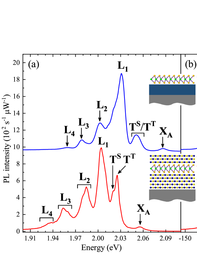
A comparison between low-temperature PL spectra measured on the WS2 monolayer deposited on SiO2/Si substrate (a "simple" structure) and on that encapsulated in hBN flakes (van der Waals heterostructure) is presented in Fig. 1. Both spectra display several emission lines with a similar characteristic pattern already reported in a number of previous works on WS2 monolayers in the "simple" [20, 21, 22, 23, 12, 24, 17, 18] and van der Waals structures [25]. In accordance with these reports, the highest energy emission peak (X) is attributed to the neutral exciton resonance. The following, lower-in-energy feature is assigned to a negative trion. A doublet structure (T and T) of this feature is not resolved in our "simple" sample but becomes apparent in the van der Waals heterostructure. Following the previous observations[15, 16, 17], the T and T emission peaks are identified as due to, correspondingly, singlet and triplet trions with two different configurations of electrons’ spins. The ability to create charged excitons in the structures under study most probably results from unintentional n-type doping of the WS2 monolayer, which is commonly reported for this material [20, 17, 18]. Notably, the (optically active) exciton (X) in WS2 monolayer is associated with the top spin-split valence band (VB) subband and the upper spin-split conduction band (CB) subband. Thus, in our case of the monolayer with a low density of remote electrons, the singlet trion involves two electrons from the same valley whereas the triplet trion comprises two electrons from different valleys - see Fig. 2(b) for a pictorial view of the intravalley singlet and intervalley triplet in a WS2 monolayer. A series of emission peaks labelled L1, L2, …, in Fig. 1 is repeatedly observed in PL spectra of WS2 (and WSe2) monolayers and attributed to recombination processes of "localized excitons"[3, 20, 26, 21, 27, 22, 28, 29, 23, 12, 24, 18, 30], though a firm character of the Ln emission series remain to be clarified in the future. Focusing on the neutral exciton peak X, we note its energy position at 2.086 eV in our "simple" structure and at 2.056 eV in the heterostructure. Those values are related to the apparent amplitudes of the exciton binding energy and the bandgap energy , (). Bearing in mind different dielectric environments of WS2 monolayers in our two samples, we expect both and to be reduced in the heterostructure as compared to the case of "simple" structure (higher polarizability of the surrounding medium for a WS2 monolayer encapsulated in hBN). A 30 meV red shift of the resonance in the heterostructure with respect to the "simple" structure indicates that the renormalization of gains over the renormalization of . Most likely, however, this gain (30 meV) represents only a small fraction of the expected changes of (and ). In similar structures but with a WSe2 monolayer, =290 meV was estimated for a monolayer placed on Si/SiO2[31] and =160 meV was extracted for the monolayer encapsulated in hBN[32]. Assuming a large (almost two times) change of also in our WS2 samples, a small difference (3 meV) in the energetic separation between X and T/T peaks observed for these two samples is surprising. This separation energy, the trion binding energy, is often assumed to be proportional to the exciton binding energy[33, 34], thought this scaling rule may not be applied to the specific case of Coulomb interaction in an anisotropic dielectric medium [14, 35, 36].
In the following, we entirely focus on the properties of negatively charged excitons (T and T) in the encapsulated WS2 monolayer. Their helicity-resolved PL spectra excited near-resonantly at an energy =2.195 eV are presented in Fig. 2(a). As schematically shown in Fig. 2(b), the appearance of trions with different spin configurations, intravalley spin-singlet T and intervalley spin-triplet T, is favourable in our sample, because the ground exciton state in monolayer WS2 is optically inactive (dark) [23, 25]. Consequently, the neutral and charged exciton complexes are excited states of the system, because the electron forming an pair is associated with the upper level in the CB [17]. An analogous situation takes place in the second tungsten-based ML, WSe2, which displays similar ordering of spin-orbit split subbands in the conduction band [23, 37, 38, 25]. In contrast, the bright MLs, MoSe2 and MoTe2, are characterised by an optically active (bright) ground-state exciton. This results in the observation of only the spin-singlet state of a charged exciton due to the Pauli exclusion principle. To analyse trions’ features in details, we fitted them with two Gaussian functions reflecting the T and T contributions, which fairly matches the experimental data (see Fig. 2(a)). We found that the linewidths of the T and T peaks are of about 5 meV, which corresponds to the recently revealed narrowing effect of encapsulation in hBN associated with the suppression of mechanisms leading to inhomogeneous broadening of excitonic emission lines [25, 39, 40].
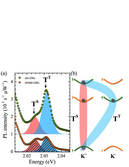
The energy separation, , between the T and T lines is found to be =70.5 meV. This value is in very good agreement with a recent assessment of =8 meV from Raman coherence measurements [41], but somewhat smaller than the value (11 meV) estimated from the deconvolution procedure of broad PL peaks [16]. As recently discussed, the amplitude of is governed by Coulomb exchange between the intravalley trion (both electrons in the same valley) and the intervalley trion (electrons in two different valleys)[42]. An additional electron in the T and T complexes formed at the same K point of the Brillouin zone occupies the same (opposite) valley for the T (T) trion (a schematic representation of possible configuration of trions is presented in Fig. 2(b)). Therefore, the coordinate parts of the wave-functions of these trions are different, they belong to different representations of the crystal symmetry group . It results in unequal exchange energy corrections for the intra- and intervalley trions, respectively (see Ref. [14] for details). Consequently, the degeneracy of the two spin configurations of the negative trion complex is lifted, higher and lower energy states are ascribed correspondingly to the intravalley (spin-singlet) and intervalley (spin-triplet) charged excitons (see Fig. 2(a)).
Next we would like to analyse in more detail the optical orientation of trions (helicity of the outgoing light with respect to the helicity of the excitation light). Both, T and T emission lines are more intense in the co-circular configuration of the excitation/emitted light as compared to the cross-circular one. This indicates a pronounced optically induced valley polarization of both excitonic transitions. Based on fitting the trions’ contribution to the PL spectrum with a combination of two Gaussian curves, we were able to determine the circular polarization degree of the emitted light defined as for each trion component, where () is the PL intensity detected in the circular polarization of the same (opposite) helicity as the excitation light. It is worth to point out that the mechanisms, which are responsible for preservation of excitonic complexes’ polarization in S-TMD monolayers have been investigated and discussed in detail in several works, [43, 44, 16]. The T line related to the spin-triplet trion displays the value of almost 50, while the T line ascribed to the spin-singlet trion is characterized by a significantly smaller , of about 16. The extracted significant difference in the efficiency of optical orientation of both trion lines is similar to that already reported in Ref. [16] (34 and 19, respectively) and indicates their different valley dephasing rates. According to Ref. [13], the fastest and hence the most efficient scattering mechanism responsible for quenching of the polarization degree of charged excitons is due to scattering of an pair between valleys, which implies that the T population feeds the T one. The process is as follow: an pair forming the T trion at the K- valley, shown in Fig. 2(b), can scatter to the opposite valley and form the T trion at the K+ point. This process is mediated by the exchange interaction towards an energetically favourable trion state. Other relaxation pathways, such as scattering of a given complex (T or T) between valleys (a simultaneous transfer of three carriers, spin flips of two electrons and a hole from one valley to another, is required) or scattering between T and T charged excitons formed at a given K± point (a spin flip of an excess electron is mandatory), are likely less efficient [13]. Therefore, each of charged exciton complexes should be characterized by a different circular polarization degree, as it can be appreciated in Fig. 2(a). Worth noting is that the value of for the neutral exciton (33, data not shown) is in our case similar to that previously reported (20 - 30) in the experiments performed on "simple" WS2 monolayers [16, 12, 30].
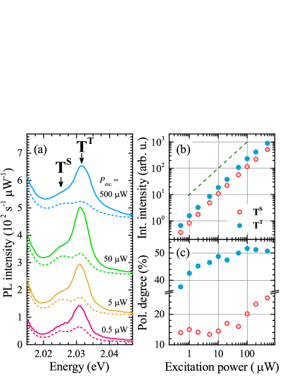
To further discuss the properties of pronounced T and T features observed in the low-temperature PL spectra of our WS2 monolayer encapsulated in hBN flakes, we will focus on the evolution of the helicity-resolved spectra with the excitation power (see Fig. 3). As illustrated in Fig. 3(a), both trions’ lines can be recognised in a whole range of the excitation power covering the change by 3 orders of magnitude (from 0.5 µW to 500 µW). The integrated intensities of the T and T peaks display a linear dependence on the excitation power (see Fig. 3(b)), as is expected for excitonic features[45]. Surprisingly, the polarization degrees of both the T and T trions, presented in Fig. 3(c), grow with increasing excitation power. A double growth of the polarization degree is seen for the intravalley T trion, while for the intervalley T complex it increases by 30 only. However, in terms of absolute values, the increases are similar and amount to about 15. As clearly visible in Fig. 3(c), there exists a distinct correlation between the changes in the polarization degree of the T and T trions. Up to about 10 µW, the polarization degree of the T complex increases with the excitation power while that of the T feature essentially remains on the same level. Beyond 10 µW, the situation inverts and now it is the T trion whose polarization degree increases whereas that of the T one progressively saturates at about 50. Worth noting is also a striking similarity between the shapes of the polarization degree versus excitation power dependences recorded for the T and T trions - with respect to the center of the figure they present mirror images one to another. In order to understand these observations one has to realize that for a given helicity of the near-resonant excitation light (addressing either the K+ or K- valley), the populations of both trion species in the complementary valley come from the intervalley scattering of photo-generated pairs. In contrast to what happens in the valley addressed by the excitation light, where, as evidenced by measurements performed in the co-circular configuration, the T complexes are being created roughly twice more efficiently than the T ones, the probabilities of converting the scattered pairs into T or T trions in the complementary valley are practically equal. That is why there is no significant difference between the intensities of the T and T contributions to the PL spectrum recorded in the cross-circular configuration (see Fig. 2(a) and dashed curves in Fig. 3(a)). By combining these two facts (approximately two times larger population of T trions in the valley addressed by the excitation light and roughly equal probabilities of creating T and T trions out of scattered eh pairs) with the values of polarization degrees observed for the T and T complexes, one can estimate that at low excitation power about 33 of photo-generated pairs is subject to the intervalley scattering. The convex (concave) shape of the polarization degree versus excitation power dependence for the T (T) trions (see Fig. 3(c)) indicates that the probabilities of creating these trions out of scattered pairs are in fact not equal, but there exists some mechanism, which gives preference to the T complexes. As can be seen, the excess amount of these trions decreases with increasing the excitation power. Last but not least, a general growth of the polarization degree with the excitation power observed for both trion species points at direct or indirect excitation-power dependence of the intervalley scattering efficiency of photo-generated pairs. Indeed, by making use of the same reasoning as presented above, one can estimate that for the highest excitation powers shown in Fig. 3(c) the amount of pairs subject to the intervalley scattering is equal to about 28. This surprisingly small change in the scattering efficiency has a profound effect on the polarization degree of both the T and T trions. To the best of our knowledge an analogous effect has not been reported so far in any S-TMD monolayer. When the excitation power is increased, a number of formed pairs grows and carriers start to occupy states characterized by larger -vectors. Consequently, one can speculate that scattering/relaxation processes become less efficient for states with larger -vectors, which enables the polarization degree of trions to increase. This supposition, though conceivable, requires, however, a theoretical justification which stays beyond the scope of the present paper.
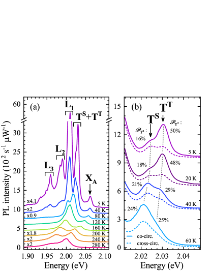
The temperature evolution of the PL spectra, excited with a moderate laser power, is shown in Fig. 4(a). As often observed[17, 18], the low energy peaks associated with "localized excitons" (L1, L2, …) are rapidly quenched with temperature and the neutral exciton emission dominates the spectra in the limit of high (room) temperature. The trion emission is also well visible, practically in a whole range of temperatures. Interestingly, each trion component displays very different behaviour. At low temperatures (up to around 20 K), the triplet (T) emission is much stronger than the singlet (T) one (see Fig. 4(b)). On the other hand, the T feature quickly disappears from the PL spectra with increasing temperature and only the T peak is observed in the temperature range above 60 K. This behaviour might be accounted in terms of efficient thermal activation/ionization of the triplet-state trion, but somewhat less efficient activation of the singlet-state trion. This reasoning is in line with the fact that the binding energy of the T trion state (energy distance to the X exciton state) is smaller than the corresponding binding energy of the T trion state. Nevertheless, a simple scheme of thermal distribution of the T, T and X states fails to account for the observed temperature evolution of the emission spectra on a quantitative level. There must be some additional effects which imply blocking of the relaxation paths between these states, in particular, likely related to an inhibition of electron spin-flip transitions involved in the T and T states. Regardless of complex physics which governs the non-thermal distribution of different excitonic complexes in our sample, which we are unable to clarify with the data in hands, it becomes apparent that the polarization degree of the T state is growing with temperature in the range when the T state progressively disappears from the spectra (see Fig. 4(b)). Thus, in agreement with our previous arguments, the polarization degree of the T trion is largely governed by the appearance of the trion triplet states. We note, however, that there must exist also other mechanisms which determine the efficiency of optical pumping in our samples. They are necessary to explain that starting from temperatures of about 60 K the polarization degree of the measured spectra progressively vanishes, reaching practically a zero level at room temperature.
Conclusions
Trion’s fine structure has been investigated in WS2 monolayers embedded between two flakes of hexagonal BN by means of helicity-resolved photoluminescence experiment. We found that at low temperatures the encapsulation of the WS2 monolayer in hBN leads to the observation of two well-resolved emission peaks due to two spin configurations of the negatively charged exciton: intervalley spin-triplet and intravalley spin-singlet. The magnitude of the splitting between them is on the order of 7 meV and both of them posses an evidently different optically induced circular polarization. An increase in temperature brings a quick disappearance of the intervalley-related line from the PL spectra, while the emission of the intravalley trion is apparent up to room temperature.
Acknowledgements
The work has been supported by the European Research Council (MOMB project no. 320590), the EC Graphene Flagship project (no. 604391), the National Science Centre (grants no. DEC-2013/10/M/ST3/00791, UMO-2017/24/C/ST3/00119), and the Nanofab facility of the Institut Néel, CNRS UGA. The support from the Fundation for Polish Science through the project "The Atomically thin semiconductors for future optoelectronics" carried out within the TEAM programme and co-financed by the European Union under the European Regional Development Fund is also acknowledged.
References
References
- [1] Kheng K, Cox R T, d’ Aubigné M Y, Bassani F, Saminadayar K and Tatarenko S 1993 Phys. Rev. Lett. 71(11) 1752
- [2] Buhmann H, Mansouri L, Wang J, Beton P H, Mori N, Eaves L, Henini M and Potemski M 1995 Phys. Rev. B 51(12) 7969
- [3] Jones A M, Yu H, Ghimire N J, Wu S, Aivazian G, Ross J S, Zhao B, Yan J, Mandrus D G, Xiao D, Yao W and Xu X 2013 Nat. Nanotechnol. 8 634
- [4] Shields A J, Pepper M, Simmons M Y and Ritchie D A 1995 Phys. Rev. B 52(11) 7841
- [5] Finkelstein G, Shtrikman H and Bar-Joseph I 1996 Phys. Rev. B 53(4) 1709
- [6] Astakhov G V, Yakovlev D R, Crooker S A, Ossau W, Christianen P C M, Rudenkov V V, Karczewski G, Wojtowicz T and Kossut J 2004 physica status solidi (c) 1 551
- [7] Ramasubramaniam A 2012 Phys. Rev. B 86(11) 115409
- [8] Liu G B, Shan W Y, Yao Y, Yao W and Xiao D 2013 Phys. Rev. B 88 085433
- [9] Kormányos A, Burkard G, Gmitra M, Fabian J, Zólyomi V, Drummond N D and Fal’ko V 2015 2D Materials 2 022001
- [10] Xu K, Wang Z, Du X, Safdar M, Jiang C and He J 2013 Nanotechnology 24 465705
- [11] Li Y, Li X, Yu T, Yang G, Chen H, Zhang C, Feng Q, Ma J, Liu W, Xu H, Liu Y and Liu X 2018 Nanotechnology 29 124001
- [12] Koperski M, Molas M, Arora A, Nogajewski K, Slobodeniuk A, Faugeras C and Potemski M 2017 Nanophotonics 6 1289
- [13] Singh A, Tran K, Kolarczik M, Seifert J, Wang Y, Hao K, Pleskot D, Gabor N M, Helmrich S, Owschimikow N, Woggon U and Li X 2016 Phys. Rev. Lett. 117(25) 257402
- [14] Courtade E, Semina M, Manca M, Glazov M M, Robert C, Cadiz F, Wang G, Taniguchi T, Watanabe K, Pierre M, Escoffier W, Ivchenko E L, Renucci P, Marie X, Amand T and Urbaszek B 2017 Phys. Rev. B 96(8) 085302
- [15] Boulesbaa A, Huang B, Wang K, Lin M W, Mahjouri-Samani M, Rouleau C, Xiao K, Yoon M, Sumpter B, Puretzky A and Geohegan D 2015 Phys. Rev. B 92(11) 115443
- [16] Plechinger G, Nagler P, Arora A, Schmidt R, Chernikov A, del Águila A G, Christianen P C, Bratschitsch R, Schüller C and Korn T 2016 Nature Communications 7 12715
- [17] Molas M R, Nogajewski K, Slobodeniuk A O, Binder J, Bartos M and Potemski M 2017 Nanoscale 9 13128
- [18] Jadczak J, Kutrowska-Girzycka J, Kapuściński P, Huang Y S, Wójs A and Bryja L 2017 Nanotechnology 28 395702
- [19] Castellanos-Gomez A, Buscema M, Molenaar R, Singh V, Janssen L, van der Zant H S J and Steele G A 2014 2D Materials 1 011002
- [20] Plechinger G, Nagler P, Kraus J, Paradiso N, Strunk C, Schüller C and Korn T 2015 Phys. Stat. Sol. RRL 9 457
- [21] Shang J, Shen X, Cong C, Peimyoo N, Cao B, Eginligil M and Yu T 2015 ACS Nano 9 647
- [22] Plechinger G, Nagler P, Arora A, Granados del Águila A, Ballottin M V, Frank T, Steinleitner P, Gmitra M, Fabian J, Christianen P C M, Bratschitsch R, Schüller C and Korn T 2016 Nano Letters 16 7899
- [23] Molas M R, Faugeras C, Slobodeniuk A O, Nogajewski K, Bartos M, Basko D M and Potemski M 2017 2D Materials 4 021003
- [24] Molas M R, Nogajewski K, Potemski M and Babiński A 2017 Scientific Reports 7 5036
- [25] Wang G, Robert C, Glazov M M, Cadiz F, Courtade E, Amand T, Lagarde D, Taniguchi T, Watanabe K, Urbaszek B and Marie X 2017 Phys. Rev. Lett. 119(4) 047401
- [26] Wang G, Bouet L, Lagarde D, Vidal M, Balocchi A, Amand T, Marie X and Urbaszek B 2014 Phys. Rev. B 90(7) 075413
- [27] Arora A, Koperski M, Nogajewski K, Marcus J, Faugeras C and Potemski M 2015 Nanoscale 7(23) 10421
- [28] Kłopotowski L, Backes C, Mitioglu A A, Vega-Mayoral V, Hanlon D, Coleman J N, Ivanov V Y, Maude D K and Plochocka P 2016 Nanotechnology 27 425701
- [29] Smoleński T, Goryca M, Koperski M, Faugeras C, Kazimierczuk T, Bogucki A, Nogajewski K, Kossacki P and Potemski M 2016 Phys. Rev. X 6 021024
- [30] Smoleński T, Kazimierczuk T, Goryca M, Molas M R, Nogajewski K, Faugeras C, Potemski M and Kossacki P 2018 2D Materials 5 015023
- [31] Raja A, Chaves A, Yu J, Arefe G, Hill H M, Rigosi A F, Berkelbach T C, Nagler P, Schüller C, Korn T, Nuckolls C, Hone J, Brus L E, Heinz T F, Reichman D R and Chernikov A 2017 Nature Communications 8 15251
- [32] Stier A V, Wilson N P, Velizhanin K A, Kono J, Xu X and Crooker S A 2018 Phys. Rev. Lett. 120(5) 057405
- [33] Stébé B and Ainane A 1989 Superlattices and Microstructures 5 545 ISSN 0749-6036
- [34] Thilagam A 1997 Phys. Rev. B 55(12) 7804
- [35] Lin Y, Ling X, Yu L, Huang S, Hsu A L, Lee Y H, Kong J, Dresselhaus M S and Palacios T 2014 Nano Letters 14 5569–5576
- [36] Kylänpää I and Komsa H P 2015 Phys. Rev. B 92(20) 205418
- [37] Zhou Y, Scuri G, Wild D S, High A A, Dibos A, Jauregui L A, Shu C, De Greve K, Pistunova K, Joe A Y, Taniguchi T, Watanabe K, Kim P, Lukin M D and Park H 2017 Nature Nanotechnology 12 856
- [38] Zhang X X, Cao T, Lu Z, Lin Y C, Zhang F, Wang Y, Li Z, Hone J C, Robinson J A, Smirnov D, Louie S G and Heinz T F 2017 Nature Nanotechnology 12 883
- [39] Cadiz F, Courtade E, Robert C, Wang G, Shen Y, Cai H, Taniguchi T, Watanabe K, Carrere H, Lagarde D, Manca M, Amand T, Renucci P, Tongay S, Marie X and Urbaszek B 2017 Phys. Rev. X 7(2) 021026
- [40] Wierzbowski J, Klein J, Sigger F, Straubinger C, Kremser M, Taniguchi T, Watanabe K, Wurstbauer U, Holleitner A W, Kaniber M, Müller K and Finley J J 2017 Scientific Reports 7 12383
- [41] Jakubczyk T, Nogajewski K, Molas M R, Bartos M, Langbein W, Potemski M and Kasprzak J 2018 2D Materials 5 031007
- [42] Yu H, Liu G B, Gong P, Xu X and Yao W 2014 Nature Communications 5 3876
- [43] Mak K F, He K, Shan J and Heinz T F 2012 Nat. Nanotechnol. 7 494
- [44] Hanbicki A T, Kioseoglou G, Currie M, Hellberg C S, McCreary K M, Friedman A L and Jonker B T 2016 Scientific Reports 6 18885 article
- [45] Klingshirn C F 2012 Springer-Verlag Berlin Heidelberg