Predicting Scattering Scanning Near-field Optical Microscopy of
Mass-produced Plasmonic Devices
Abstract
Scattering scanning near-field optical microscopy enables optical imaging and characterization of plasmonic devices with nanometer-scale resolution well below the diffraction limit. This technique enables developers to probe and understand the waveguide-coupled plasmonic antenna in as-fabricated heat-assisted magnetic recording heads. In order validate and predict results and to extract information from experimental measurements that is physically comparable to simulations, a model was developed to translate the simulated electric field into expected near-field measurements using physical parameters specific to scattering scanning near-field optical microscopy physics. The methods used in this paper prove that scattering scanning near-field optical microscopy can be used to determine critical sub-diffraction-limited dimensions of optical field confinement, which is a crucial metrology requirement for the future of nano-optics, semiconductor photonic devices, and biological sensing where the near-field character of light is fundamental to device operation.
I Introduction
Today’s optic, photonic, and plasmonic devices incorporate light into nanoscale devices that enable diverse new functionality for chemical or biological sensing and imaging Jeanmaire and Van Duyne (1977), precision light sources Painter et al. (1999); Oulton et al. (2009); Zhu et al. (2015), silicon photonics-based communications and signal processing Yariv and Yeh (2007), and data storage Stipe et al. (2010); Challener et al. (2009). These devices are often critically dependent on the behavior of light well below the diffraction limit, and therefore require robust near-field characterization techniques, linked with numerical predictions and validations, to design and fabricate functioning devices. This requirement becomes even more essential when such devices are to be manufactured in massive quantities that require process quality control. In fact, future hard disk drives (HDDs) will rely on near-field optical heaters for data storage, and the successful development and production of novel HDD magneto-optical write heads is largely contingent on the ability to reliably predict and validate the near-field behavior of as fabricated devices by direct experimental characterization. The technical improvements to scattering scanning near-field optical microscopy that we have developed for HDD write head optical antenna characterization are potentially extensible and beneficial to any field of study involving the direct optical measurement of photonic modes arising in proximity to nanoscale features.
II Heat Assisted Magnetic Recording Background
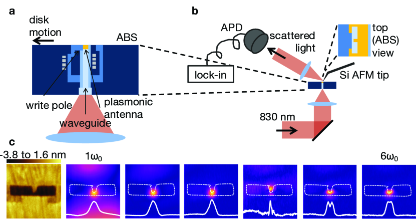
Despite alternative technology developments, most of the world’s increasing data storage demands are still satisfied by HDDs. To improve efficiency, the HDD industry has encountered and worked to overcome fundamental limitations preventing the further areal density growth on a disk of magnetic material Stipe et al. (2010); Challener et al. (2009); Lu and Charap (1994); Weller and Moser (1999); Zhou et al. (2014a). Currently used magnetic media cannot support smaller bit sizes (known as the superparamagnetic limit, smaller bits are less stable), but magnetically harder media has proven too difficult to write (alter magnetization) using traditional magnetic write head strengths/capabilities. In order for data to be recorded into this media, a local spot on the disk with dimensions of the desired bit size (10s of nanometers) must be heated close to its Curie temperature resulting in a significant drop of its magnetic coercivity, thus allowing the magnetic polarization to be switched under the applied field. The chosen method for locally heating the magnetic media in under-development devices is a plasmonic antenna, which focuses far-field optical light into high-intensity and rapidly decaying near-field optical energy, which is directed onto the recording medium (Figure 1a). The high-intensity near-field energy is capable of heating the magnetic media (only a few nanometers away) to the desired temperature while the rapid decay of the evanescent field ensures that the thermal gradient in the media is large so the resulting bit size is comparable to the size of the antenna and its near-field “spot.” During drive operation the media is a fast-rotating disk, and as the disk rotates, the magnetic grains in the heated spot experience an applied magnetic field from the write pole, thereby switching their magnetization. Upon further disk rotation, the recorded bit is removed from the near-field hot spot, cools, and the magnetization is therefore “frozen” into the media. This technology is known as heat-assisted magnetic recording (HAMR), and it is capable of achieving the desired smaller bit sizes and higher areal densities Stipe et al. (2010); Challener et al. (2009).
Designing, developing, and fabricating the HAMR technology has numerous challenges associated with the newly integrated laser, photonic, and plasmonic elements in addition to the magnetic elements already present. While electromagnetic simulations are immensely powerful and able to guide design and predict results, experimental characterization techniques are necessary to verify modeling results when compared to empirical observations of as-fabricated devices, which can be subjected to many variations, and to determine failure mechanisms. In HAMR, the introduction of a plasmonic antenna generating a deep subwavelength near-field spot calls for a characterization technique capable of investigating the properties and consistency of this crucial feature of the HAMR head’s performance. Former work has demonstrated scattering scanning near-field optical microscopy (sSNOM) to be a top candidate for this task Zhou et al. (2014a); Hillenbrand and Keilmann (2000); Dorfmüller et al. (2009); Imura et al. (2004); Taubner et al. (2005); Rang et al. (2008); Esteban et al. (2008); Schnell et al. (2010); Zhou et al. (2014b).
III Scattering Scanning Near-field Optical Microscopy Background
SNOM was originally developed as a probe system with an aperture in a diaphragm Ash and Nicholls (1972); Lewis et al. (1984), which later was traded for a tapered optical fiber coated with metal such as gold, silver, or aluminum Pohl et al. (1984); Betzig and Trautman (1992); Betzig and Chichester (1993). Propagating far-field light inside the fiber is converted to near-field radiation by the angled metal coating and then illuminates the sample. This probe also serves to convert the sample-interacted near-field back into propagating far-field light, which would be observed back through the optical fiber. However, the resolution limit of apertured SNOM is determined by the dimensions of the aperture and the excitation wavelength so that as the aperture shrinks, the amount of electromagnetic energy coupled through the aperture and transmitted to the far-field falls off precipitously according to the Bethe limit () Bethe (1944). (Bethe’s analytical near-the-hole solutions were later corrected by Bouwkamp Bouwkamp (1950), and a modern discussion is provided by Novotny et al. Novotny and Hecht (2012)) As a result, for small aperture sizes, the near-field signal accessible using an aperture probe falls below the background and noise thresholds for the technique, thus limiting resolution of apertured SNOM to 50 nm for visible or near-infrared light. Because the HAMR plasmonic antennas are generally smaller than this size, a technique offering better resolution is necessary.
In sSNOM, the resolution of the SNOM technique is increased by incorporating an atomic force microscopy (AFM) scan probe tip that scatters, rather than transmits, the near-field light into the far-field, thus causing the sharpness of the AFM probe to determine the resolution rather than the size of the aperture and the wavelength Wickramasinghe and Williams (1990); Zenhausern et al. (1995); Lahrech et al. (1996); Knoll and Keilmann (1999). For sub-ten-nanometer tip radii, the scattering cross-section of light is still more than sufficient to beat the signal-to-noise and signal-to-background limits when using a lock-in amplifier to detect the light scattered from the tip Hillenbrand and Keilmann (2000). In the case of metallic or metal-coated tips, the tip both generates the probing near-field (through the “lightning rod” or “nanofocusing” effect)Martin et al. (2001); Stockman (2004) and performs the function of a dipole scatterer by converting the sample-interacted near-field radiation back into far-field light that can be collected by an objective Zenhausern et al. (1995); Lahrech et al. (1996); Knoll and Keilmann (1999). However, for HAMR plasmonic antennas (as well as for other general plasmonic structures), the near-field is generated by the sample (excited by an external source), and so tips with minimal signal disruption while still maintaining high scattering cross-sections are desired Dorfmüller et al. (2009). In this work, uncoated silicon tips with a typical radius of 5-15 nm and optically accessible tip apexes were used.
Given the large amount of background scattered light that is generally present in sSNOM measurements, the signal specific to the tip apex can be extracted through the use of a lock-in amplifier tuned to the fundamental and higher harmonics of the AFM tip cantilever’s resonant oscillation frequency Hillenbrand and Keilmann (2000); Bek et al. (2006). Prior work has demonstrated that the lower order harmonics include both the propagating and evanescent components of the scattered light, while the higher order harmonics have a stronger dependence on the near-field strength and hence contain higher contrast near-field information Hillenbrand and Keilmann (2000). The sSNOM system used to measure the HAMR plasmonic antennas (Figure 1b) in this work uses this lock-in driven technique and is capable of capturing up to three harmonics simultaneously during AFM measurements (Figure 1c).
IV Predicting Behavior of Mass-produced Plasmonic Devices
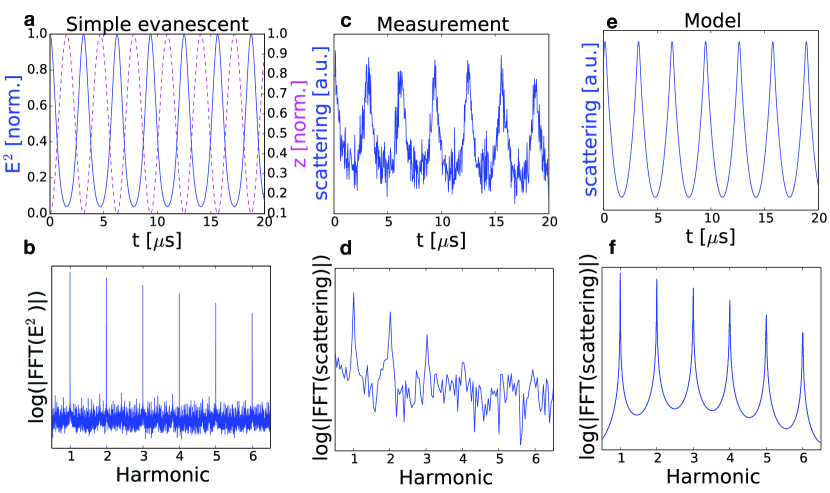
In order to use sSNOM to guide the design and development of HAMR devices, we developed a model to map the electric field data from electromagnetic simulations into the expected harmonic mappings generated by the sSNOM system. The first stage began with a few general approximations. It was assumed that the position of the AFM tip varied sinusoidally in time with the resonant frequency of the cantilever (), that the evanescent electric field followed an exponential decay with increasing distance from sample surface (), and that the scattering was proportional to intensity (). As expected, the model yields maximum scattering intensity when the tip is closest to the surface (Figure 2a, here = 300 kHz), and a fast Fourier transform (FFT) of the scattered field yields harmonics that decay exponentially in intensity with increasing order. Using the sSNOM system and oscilloscope capabilities of the lock-in amplifier software, a scattering signal similar in shape to that of the simple evanescent approximation was observed when the tip was hovered (oscillating) over the center feature of the plasmonic antenna containing the most intense near-field signal (Figure 2c). Despite the noise present in this data, a numerical FFT still reveals several harmonics (Figure 2d). It is worth noting that this FFT is performed through numerical analysis of the captured time-domain oscilloscope trace, not by the lock-in amplifier hardware. The lock-in harmonic acquisition during imaging was performed with sufficiently long time constants in order to improve the signal-to-noise ratio in the higher harmonics significantly above the threshold apparent in this post-processed FFT trace.
Because the sSNOM system and HAMR devices are considerably more complex than the simple evanescent model, further improvements to the model were made to better match experimental conditions. To substitute for the simple evanescent electric field assumption (), data from electromagnetic simulations were introduced to account for the actual field expected for the as-designed dimensions of the HAMR plasmonic antenna. The tip-sample interaction was then accounted for in two stages. The first stage weights each 1 nm 1 nm -column (where the column is aligned normal to the surface of the sample) of simulated electric field data by a scattering parameter : Schnell et al. (2010); Knoll and Keilmann (1999, 2000); Bouhelier et al. (2003)
| (1) |
which yields the scattering parameter adjusted electric field. The scattering parameter is derived from a spherical probe and image dipole interaction and is defined by the following set of equations: Ash and Nicholls (1972); Zenhausern et al. (1995); Knoll and Keilmann (1999)
| (2) | ||||
where is the effective polarizability of the tip-sample combination, is the polarizability of the silicon tip (approximated here as a sphere), is the free space wavelength of the incident light, and and are the complex dielectric functions of the tip and sample, respectively. was allowed to vary based on the material (either gold, oxide, or magnetic material) located directly below the -column being computed.
After applying the scattering transformation to the electric field, the second stage accounted for the shape of the tip. Planar slices of the resulting weighted electric field parallel to the air-bearing surface (ABS), which is the surface facing the rotating magnetic media containing the plasmonic antenna (in the plane), were serially convolved with two matrices with each representing different components of the shape of the AFM tip. One matrix was designed as a cone to represent the shape of the tip’s shaft, and the other matrix was designed as a top-hat to represent the shape of the end of the tip. After these convolutions, for a 1 nm 1 nm -column positioned directly above the plasmonic antenna, it can be seen that the modeled time-dependent scattered field (Figure 2e) more closely matches the shape of the measured scattered field of the sSNOM signal (Figure 2c) than does the scattered field resulting from the simple evanescent model (Figure 2a). Similarly, a FFT of this modeled sSNOM signal (Figure 2f) mimics the behavior of the measured signal from the lock-in amplifier (Figure 2d) yielding smooth harmonic spikes, and when performed over the entire plane, yields the desired modeled near-field harmonic mappings.
V Effects of the AFM Tip’s Shape
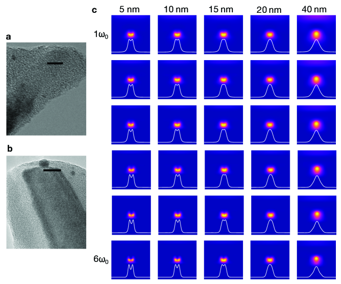
Development of the sSNOM model required further investigation of the AFM tip’s local shape interacting with the high-intensity near-field. Based on manufacturer specifications, our experience, and previous transmission electron microscopy (TEM) images, it was assumed that most tips used in these experiments contained a 5-15 nm radius, where the sharper tips (5 nm radius, Figure 3a) gave a sSNOM signal with better resolution than average (10 nm radius, Figure 3b) or blunter (15 nm radius) tips. Furthermore, TEMs of tips imaged post-scanning revealed several nanometers of material built up on the tip, including in the region separating the silicon tip from the sample. Therefore, the corresponding change in tip-sample separation was accounted for in the sSNOM model in addition to the tip’s radius. The TEM images also revealed the angled nature of the used tip’s shaft as well as the flat top-hat nature of its end.
Both the shape of the tip’s shaft as well as its end were incorporated into the sSNOM model through the two convolution matrices described above. The shaft was approximated as a cone with a half-angle of 9∘, and the tip end was approximated as a top-hat (step function in cylindrical coordinates) with variable radius. Radii of 5, 10, and 15 nm represented the range of usual tips while radii of 20 and 40 nm represented more extreme cases of blunt tips (Figure 3c). Based on the developed sSNOM model and previous experience with these tips, a radius of 15 nm was used in the model for correlation with the experimental data. Further improvement of the model is possible through the use of a three-dimensional volumetric convolution, rather than two-dimensional planar convolution used in this work, of the conical tip shaft matrix (including the tip’s angled rather than vertical approach) with the scattered field, which is expected to more accurately model the physical configuration and may increase the far-field contribution to the .
VI Effects of the AFM Tip’s Distance of Closest Approach
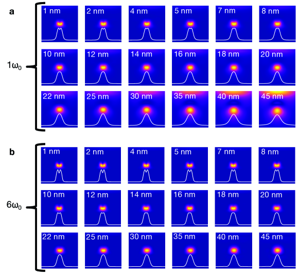
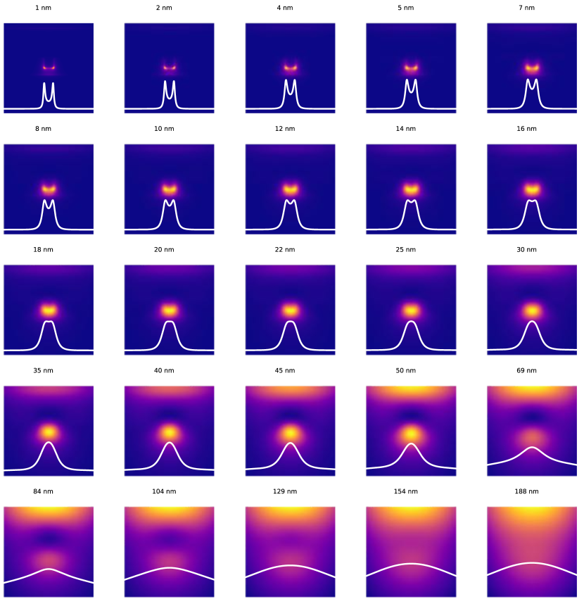
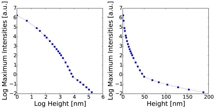
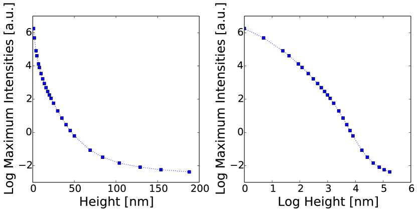
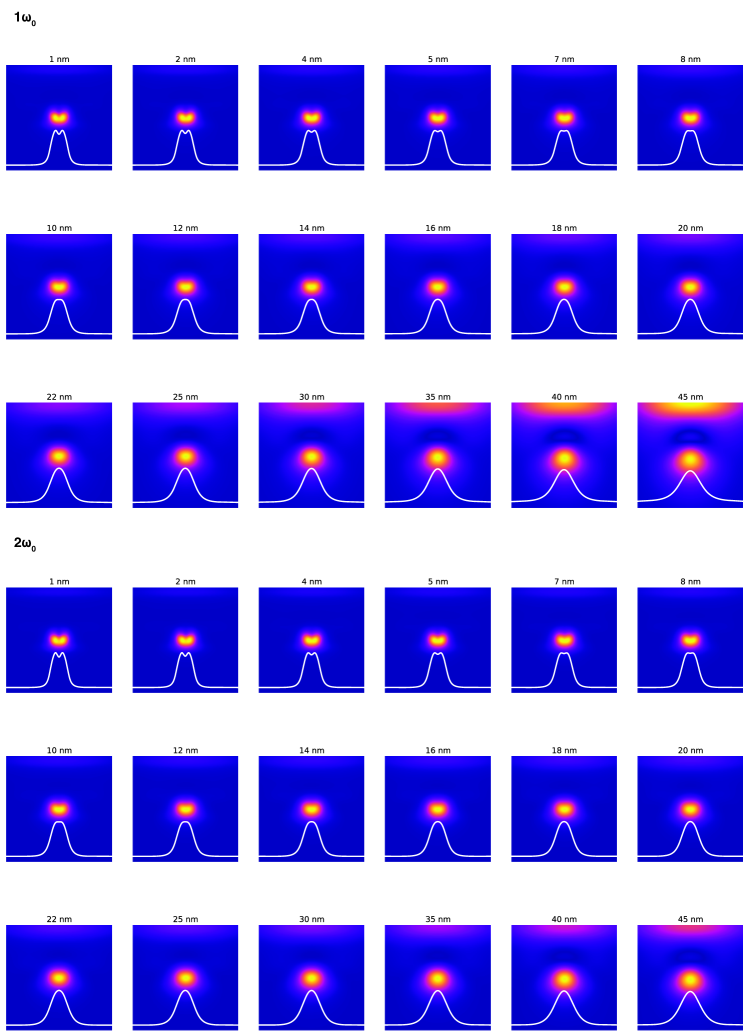
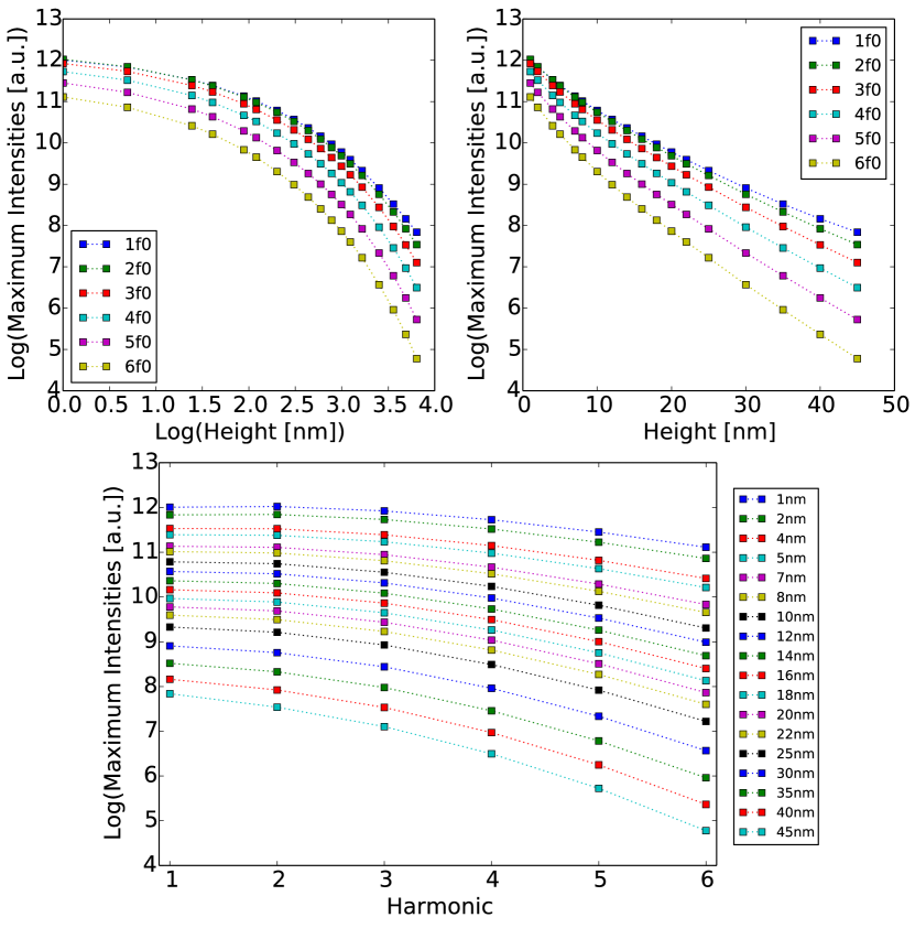
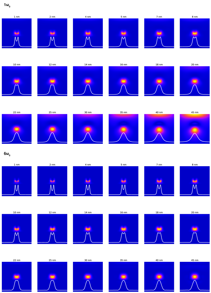
Further investigation of the mechanical AFM behavior of the sSNOM system was performed in order to determine the tip’s distance of closest approach (DCA) to the sample. In the sSNOM model, the DCA value was set as the minimum height (and cutoff) for the FFTs of the scattered signal. It was found that the chosen DCA had a significant effect on the sSNOM model’s results (Figure 4). A smaller DCA (tip approaches much closer to the ABS) incorporates much more of the dominant near-field signal (as opposed to the weaker far-field signal) into the FFT, which becomes evident in the harmonic maps for the fundamental frequency (, Figure 4a) when compared with the higher frequency (Figure 4b). Maximum intensity plots are also included for all investigated harmonics and heights as well as additional harmonic maps in the Supplemental Information (Figures S1-S3).
Estimation of tip DCA was also performed with a mechanical model of tapping mode AFM, which solves the equation of motion for the cantilever numerically as it encounters tip-sample forces modeled to include van der Waals attraction, capillary adhesion due to a water layer, and Pauli hard sphere repulsion Chen et al. (2004). When inputting the tip radius, free amplitude, and amplitude setpoint (see Supplementary Information), and using the measured phase signal as a check for accuracy, the model shows that the cantilever was oscillating in the repulsive regime indicating that the tip approaches the surface very closely and experiences repulsive contact with the sample at the bottom of most oscillations.
VII Results
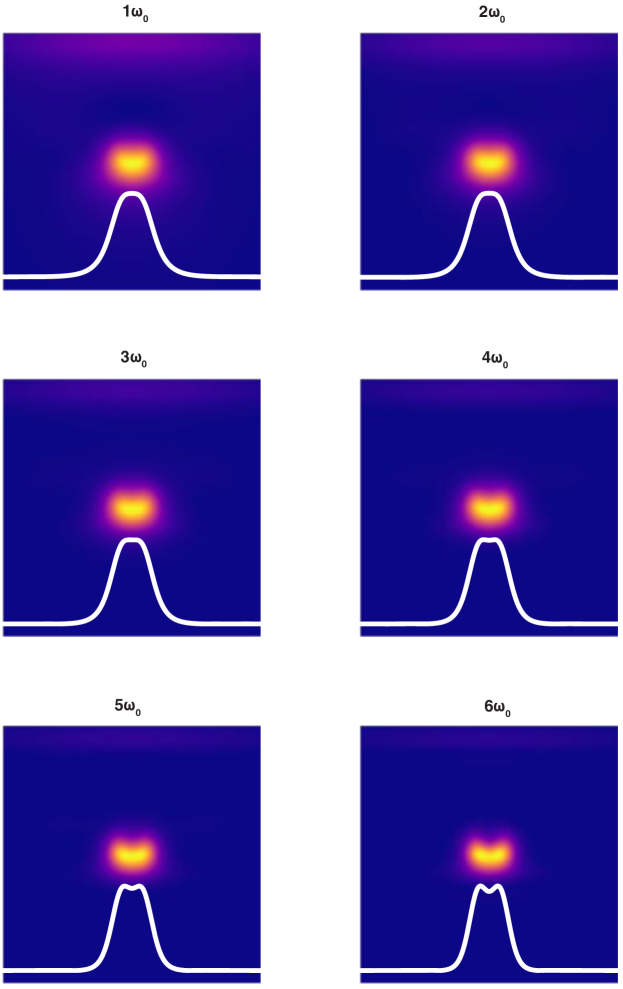
Accounting for the thickness of material collected by the tips during scans (5 nm in Figure 3a,b) as well as other complex effects due to the water meniscus between the tip and the sample surface Chen et al. (2004); Calleja et al. (2002), and comparing the experimentally measured data with the sSNOM model’s results, a DCA of 8 nm was chosen together with a tip radius of 15 nm to represent the best fit of the sSNOM model to the experimental measurements and expectations. A “good fit” between the harmonic maps generated by the sSNOM model and the experimental data was established when a bifurcated near-field signal was observed in the higher order harmonics (, ) but not in the lower order harmonics (). The visible near-field bifurcation requirement for the higher harmonics ruled out the possibility of the experimental tip having a radius of 20 nm or larger since no bifurcation was evident, even in the (Figure S4), when the chosen distance of closest approach was 1 nm (the closest possible in the present model). In addition, good qualitative agreement between the experimental and modeled near-field maps using smaller tip radii (15 nm) required DCA values exceeding expectations and so were ruled out by the AFM mechanical model (Figures S5-S9). Since the sSNOM model’s results show significant dependence on the DCA, incorporating simulated electric field data with topographic sensitivity (the presented simulations assumed a planar surface) would more closely match the experimental conditions revealed by the recessed nature of the waveguide relative to the antenna seen in the AFM image and could improve the model.
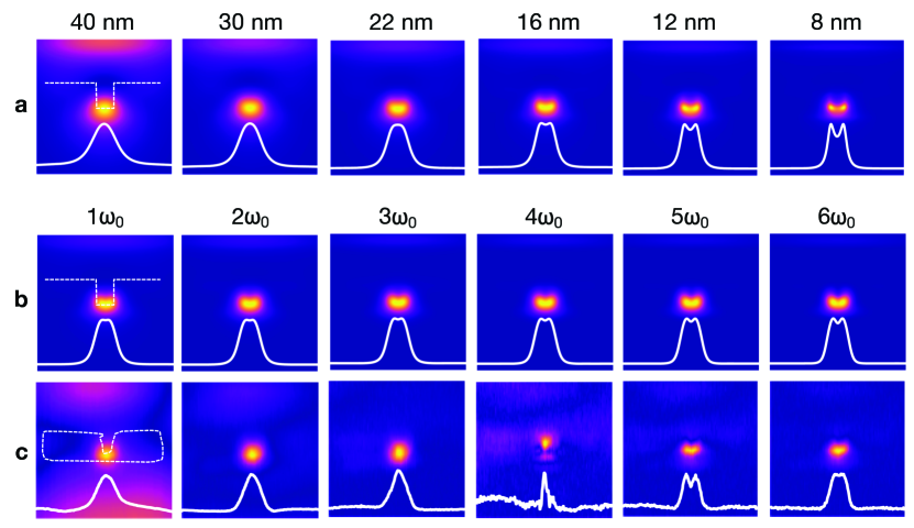
Slices of the simulated electric field intensity at different heights of interest (Figure 5a, with further details included in the Supplemental Information are compared to the corresponding harmonics from the sSNOM model results using a tip radius of 15 nm and a DCA of 8 nm (Figure 5b) and the experimentally measured harmonic maps (Figure 5c). From this comparison, it can be seen that higher harmonics, such as and , are more representative of the near-field in the region that would be occupied by the magnetic media during drive operation than their lower order harmonic counterparts. The nature of the higher order harmonics in which this relationship was found signified the prescribed rapid change in near-field intensity closer to the plasmonic antenna. The strange behavior exhibited by the measured was likely caused by a non-sinusoidal feature at the bottom of the tip’s oscillation due the tip’s possible contact with and/or repulsion by the sample surface during its motion. The non-sinusoidal motion of the tip was not accounted for in the present sSNOM model, but it could be introduced upon further mechanical characterization of the sSNOM-tip system and its interaction with the sample. An introduction of a sharp change in the peak scattering would surely become evident in one or more of the higher order harmonics in the presence of non-sinusoidal tip oscillation. In the case of this experiment, this feature was found in the , and it is also expected to have been present in the , etc. This observation as well as the AFM mechanical model results and the flat nature of the post-scanning tips suggests that the scan parameters cause significant tip interaction with the sample likely leading to the tip’s top-hat shape. Scan parameters for typical non-contact tip operation involve small oscillation amplitudes that fail to sweep sufficient evanescent field variation and are not capable of performing the desired full characterization of the plasmonic antenna’s near-field. For this reason, large oscillation amplitudes were used that resulted in greater tip-sample interactions.
In conclusion, sSNOM is a useful technique capable of characterizing HAMR heads for next-generation hard disk drives. The development of a sSNOM model to translate from simulated electric field data was necessary in order to derive meaning from the measured near-field harmonics. Furthermore, the same model approach can be applied to other plasmonic structures across many disciplines and applications.
VIII Methods
Steady state electromagnetic modeling of the plasmonic system was performed using the FDTD method in Lumerical.
sSNOM measurements were performed with the AIST-NT CombiScope 1000-SPM and tips from Nanosensors (ATEC-NC). The auto non-contact/tapping default mode was used with the 160 m cantilevers (300 kHz resonance), 80 nm oscillation amplitude, and 87 percent set point. An 830 nm laser (diode: Sanyo DL8142-201) was polarized (Thorlabs LPVIS100-MP) and directed with free space optics into the microscope. The microscope’s bottom objective (Olympus ULWD MSPlan 50) mount was piezo tuned in three dimensions first for coarse alignment and then for optimal coupling of the laser spot into the waveguide once the tip was hovered over the plasmonic antenna. A 50 objective (Mitutoyo NIR M Plan Apo NIR 50, 378-825-5) was precisely aligned with piezo scanners (in objective’s plane, manual in ) and used to collect the scattered light, which was then observed by an APD (Thorlabs APD120A). The resulting signal passed through a lock-in amplifier (Zurich Instruments HF2LI), and data was collected through the AIST-NT software.
IX Acknowledgements
L.M.O. acknowledges the National Institutes of Health Biotechnology Training Grant (T 32 GM008347) and the National Science Foundation Graduate Research Fellowship Program (00039202). Work performed at the Molecular Foundry (TEM images and AFM mechanical model) was supported by the Office of Science, Office of Basic Energy Sciences, of the U.S. Department of Energy under contract no. DE-AC02-05CH11231.
References
- Jeanmaire and Van Duyne (1977) D. L. Jeanmaire and R. P. Van Duyne, Journal of Electroanalytical Chemistry 84, 1 (1977).
- Painter et al. (1999) O. Painter, R. K. Lee, A. Scherer, A. Yariv, J. D. O’Brien, P. D. Dapkus, and I. Kim, Science 284, 1819 (1999).
- Oulton et al. (2009) R. F. Oulton, V. J. Sorger, T. Zentgraf, R.-M. Ma, C. Gladden, L. Dai, G. Bartal, and X. Zhang, Nature 461, 629 (2009), arXiv:0509168v1 [quant-ph] .
- Zhu et al. (2015) H. Zhu, Y. Fu, F. Meng, X. Wu, Z. Gong, Q. Ding, M. V. Gustafsson, M. T. Trinh, S. Jin, and X.-Y. Zhu, Nature Materials 14, 636 (2015).
- Yariv and Yeh (2007) A. Yariv and P. Yeh, Photonics, 6th ed. (Oxford University Press, Inc., New York, New York, 2007).
- Stipe et al. (2010) B. C. Stipe, T. C. Strand, C. C. Poon, H. Balamane, T. D. Boone, J. A. Katine, J.-L. Li, V. Rawat, H. Nemoto, A. Hirotsune, O. Hellwig, R. Ruiz, E. Dobisz, D. S. Kercher, N. Robertson, T. R. Albrecht, and B. D. Terris, Nature Photonics 4, 484 (2010).
- Challener et al. (2009) W. A. Challener, C. Peng, A. V. Itagi, D. Karns, W. Peng, Y. Peng, X. Yang, X. Zhu, N. J. Gokemeijer, Y.-T. Hsia, G. Ju, R. E. Rottmayer, M. A. Seigler, and E. C. Gage, Nature Photonics 3, 303 (2009).
- Lu and Charap (1994) P.-L. Lu and S. H. Charap, Journal of Applied Physics 75, 5768 (1994).
- Weller and Moser (1999) D. Weller and A. Moser, IEEE Transactions on Magnetics 35, 4423 (1999).
- Zhou et al. (2014a) N. Zhou, X. Xu, A. T. Hammack, B. C. Stipe, K. Gao, W. Scholz, and E. C. Gage, Nanophotonics 3, 141 (2014a).
- Hillenbrand and Keilmann (2000) R. Hillenbrand and F. Keilmann, Physical Review Letters 85, 3029 (2000).
- Dorfmüller et al. (2009) J. Dorfmüller, R. Vogelgesang, R. T. Weitz, C. Rockstuhl, C. Etrich, T. Pertsch, F. Lederer, and K. Kern, Nano Letters 9, 2372 (2009).
- Imura et al. (2004) K. Imura, T. Nagahara, and H. Okamoto, Journal of Physical Chemistry B 108, 16344 (2004).
- Taubner et al. (2005) T. Taubner, F. Keilmann, and R. Hillenbrand, Optics Express 13, 8893 (2005).
- Rang et al. (2008) M. Rang, A. C. Jones, Z. Fei, Z. Y. Li, B. J. Wiley, X. Younan, and M. B. Raschke, Nano Letters 8, 3357 (2008).
- Esteban et al. (2008) R. Esteban, R. Vogelgesang, J. Dorfmüller, a. Dmitriev, C. Rockstuhl, C. Etrich, and K. Kern, Nano Letters 8, 3155 (2008).
- Schnell et al. (2010) M. Schnell, A. Garcia-Etxarri, J. Alkorta, J. Aizpurua, and R. Hillenbrand, Nano Letters 10, 3524 (2010).
- Zhou et al. (2014b) N. Zhou, Y. Li, and X. Xu, Optics Express 22, 18715 (2014b).
- Ash and Nicholls (1972) E. A. Ash and G. Nicholls, Nature 237, 510 (1972).
- Lewis et al. (1984) A. Lewis, M. Isaacson, A. Harootunian, and A. Muray, Ultramicroscopy 13, 227 (1984), arXiv:arXiv:1011.1669v3 .
- Pohl et al. (1984) D. W. Pohl, W. Denk, and M. Lanz, Applied Physics Letters 44, 651 (1984).
- Betzig and Trautman (1992) E. Betzig and J. K. Trautman, Science 257, 189 (1992).
- Betzig and Chichester (1993) E. Betzig and R. J. Chichester, Science 262, 1422 (1993).
- Bethe (1944) H. A. Bethe, Physical Review 66, 163 (1944).
- Bouwkamp (1950) C. J. Bouwkamp, Philips Research Reports 5, 321 (1950).
- Novotny and Hecht (2012) L. Novotny and B. Hecht, in Principles of Nano-Optics (Cambridge University Press, Cambridge, UK, 2012) 2nd ed., Chap. 6, pp. 170–183.
- Wickramasinghe and Williams (1990) H. K. Wickramasinghe and C. C. Williams, “Apertureless near field optical microscope,” (1990).
- Zenhausern et al. (1995) F. Zenhausern, Y. Martin, and H. K. Wickramasinghe, Science 269, 1083 (1995).
- Lahrech et al. (1996) A. Lahrech, R. Bachelot, P. Gleyzes, and A. C. Boccara, Optics Letters 21, 1315 (1996).
- Knoll and Keilmann (1999) B. Knoll and F. Keilmann, Nature 399, 7 (1999).
- Martin et al. (2001) Y. C. Martin, H. F. Hamann, and H. K. Wickramasinghe, Journal of Applied Physics 89, 5774 (2001).
- Stockman (2004) M. I. Stockman, Physical Review Letters 93, 137404 (2004).
- Bek et al. (2006) A. Bek, R. Vogelgesang, and K. Kern, Review of Scientific Instruments 77, 043703 (2006).
- Knoll and Keilmann (2000) B. Knoll and F. Keilmann, Optics Communications 182, 321 (2000).
- Bouhelier et al. (2003) A. Bouhelier, M. R. Beversluis, and L. Novotny, Applied Physics Letters 82, 4596 (2003).
- Chen et al. (2004) L. Chen, L. C. Chin, P. D. Ashby, and C. M. Lieber, Nano Letters 4, 1725 (2004).
- Calleja et al. (2002) M. Calleja, M. Tello, and R. García, Journal of Applied Physics 92, 5539 (2002).
X Supplemental Information
This supplemental information contains additional modeled near-field mappings as well as other graphs to more fully show how the modeled results change with different values used for the input parameters (tip radius, distance of closest approach – DCA) and support paper conclusions.
X.1 Additional Mappings for the Parameters Chosen in the Main Text (15 nm radius, 8 nm DCA)
![[Uncaptioned image]](/html/1802.05259/assets/x7.png)
![[Uncaptioned image]](/html/1802.05259/assets/x8.png)
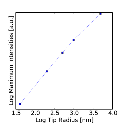
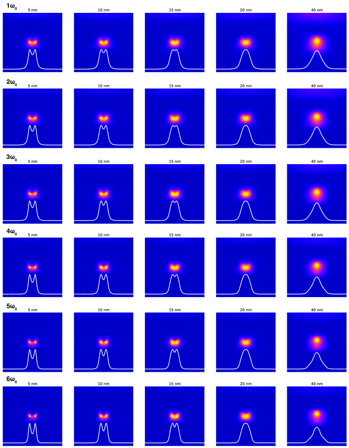
X.2 Figures for Observing Trends in the Maximums of Each Mapping as a Function of DCA Height, Tip Radius, and Harmonic
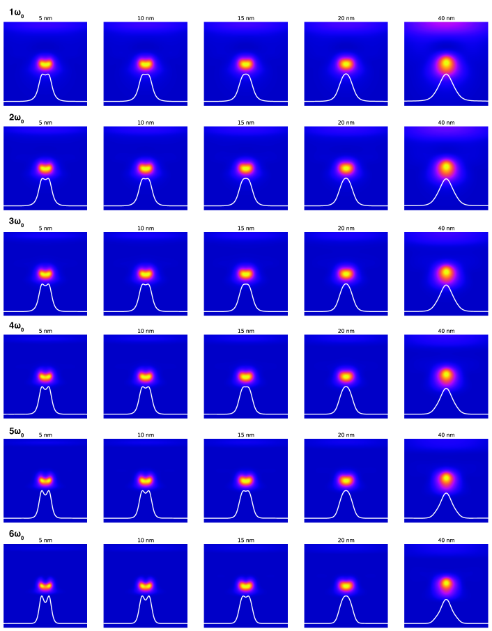
X.3 Near-field Mappings for Other Modeled Tip Radii
![[Uncaptioned image]](/html/1802.05259/assets/x11.png)

X.4 Near-field Mappings for Other Modeled Distances of Closest Approach
X.5 Simulated Electric Field Intensity