2D-3D crossover in a dense electron liquid in silicon
Abstract
Doping of silicon via phosphine exposures alternating with molecular beam epitaxy overgrowth is a path to Si:P substrates for conventional microelectronics and quantum information technologies. The technique also provides a new and well-controlled material for systematic studies of two-dimensional lattices with a half-filled band. We show here that for a dense ( cm-2) disordered two-dimensional array of P atoms, the full field angle-dependent magnetostransport is remarkably well described by classic weak localization theory with no corrections due to interaction effects. The two- to three-dimensional cross-over seen upon warming can also be interpreted using scaling concepts, developed for anistropic three-dimensional materials, which work remarkably except when the applied fields are nearly parallel to the conducting planes.
pacs:
72.15.Rn, 73.50.Jt, 71.10.Ay, 81.15.-zI Introduction
The possibility of using single phosphorus (P) atoms in silicon as qubit hosts has driven the development of a fabrication technology for deterministic placement of the dopants which is very different from ordinary ion implantation/annealing paradigms. Hydrogen-passivated surfaces of Si(100) wafers are edited using a scanning tunneling microscope tip which removes protons, leaving behind exposed regions of silicon which can selectively bind phosphine (PH3) molecules to incorporate P in the semiconductor. Subsequent annealing and silicon deposition then yield encapsulated two-dimensional P structures; iteration of all steps in this process can provide three-dimensional devicesSchofield:2003fk ; Scappucci:2015fk .
Important components of any integrated electronic device technology are highly conducting sheets which can serve as current vias or capacitance/shielding plates, and this is accomplished by simply exposing large unpassivated areas of Si to phosphine. The result is very heavily doped two-dimensional silicon, with typically 1/180 P atoms/Si atom. For comparison, the solubility limit of P in bulk CZ-grown Si is 1/450 – 1/250 impurities/Si atomsChiou:2000fk ; McKibbin:2014ng , and the highest densities for activated subsurface ion implanted layers correspond to 1/80 P/SiSolmi:1996fv . Furthermore, for the two-dimensional electron gases produced in Si MOSFETs the carrier densities are typically 1012–1013 cm-2, corresponding to 1/5–1/5 electrons/Si, where we assume an inversion layer thickness of 10 nm. Typical parameters for some 2D systems appear in Table 1 and it is apparent the -layer technique produces the densest 2D systems while retaining the coherence characteristics.
| 2D system | |||||
|---|---|---|---|---|---|
| [nm] | [nm] | [cm-2] | [cm-3] | [nm] | |
| Ge:P -layerScappucci:2015fk | 5 | 184 | 0.63 | 0.45 | 1.49 |
| Current work | 15 | 320 | 2.8 | 0.28 | 10 |
| Si MOSFETWheeler:1981fk | 48 | 252 | 0.07 | 0.007 | 10 |
| QW 2DHGSimmons:2001td | 26 | 61 | 4.510-4 | 2.2510-5 | 20 |
| GrapheneLara-Avila:2011zl | 50 | 900 | 0.005 | 0.005 | 1 |
Beyond their potential for conventional and quantum electronics, the P -layers are of fundamental physical interest because they realise a disordered two-dimensional Hubbard model where the sites are provided by the P dopants. The unprecedented high density allows access to what should be the simple (disordered) Fermi liquid regime for large t/U where t is the hopping integral and U is the on-site Coulomb interaction, where classical weak-localization (WL) theory should become exact.
We have consequently set out to test this hypothesis, taking advantage not only of high quality -layers of phosphorus in silicon, but also of a modern vector magnet which allows fields to be applied in arbitrary directions under software control. The density of dopants in the conducting slab in our sample corresponds to a typical interimpurity spacing of 1.5 nm which is approximately the Bohr radius for P in Si. Theoretical estimatesSaraiva:2015fk ; Le:2017eh of the Hubbard model parameters for Si:P show for inter-impurity spacing of 0.75 nm the unscreened on-site energy meV would be similar to the tunnelling rate . Additionally some reduction of is expected due to screening and hence it is likely that the experimental regime that we study here is well described by the metallic regime of the Hubbard modelGeorges:1996dmft . On this backdrop, the focus of this study is a full temperature, magnitude and angle-dependent magnetoconductance (MC) set of experiments showing unprecedentedly rigorous demonstration of the validity of WL theory in two dimensions, including the remarkably simple formula where the in-plane field component, due to the thickness of the finite -layer, simply increases the inelastic scattering rate to be inserted into the Hikami-Larkin-Nagaoka WL formulaHikami:1980vn form (which is valid in the limit of zero thickness and depends only on the perpendicular component):
| (1) |
where is the inelastic scattering time and is the additional phase-breaking time due to . Mensz and WheelerMensz:1987fk originally demonstrated the applicability of Equation 1 for silicon MOSFETs in tilted fields, and Mathur and BarangerMathur:2001fr later added substantial theoretical justification.
The form of the Hikami-Larkin-Nagaoka formula with , where and are not interchangeable, is qualitatively different from anisotropic three-dimensional metals where the field components are interchangeable. We have exploited the vector magnet to explore the growth of this difference on cooling, and have discovered another remarkably simple form which characterizes all data except those with B nearly parallel to the planes:
| (2) |
In the limit where the dephasing length is short compared to the magnetic length (where is the magnetic flux quantum), the power-mean approaches unity, meaning that conductances affected by scattering parallel and perpendicular to the plane simply add as for parallel resistor shunts. In the opposite limit, becomes very large, meaning that whichever conductance is larger, namely that due either to in-plane or out-of-plane scattering, dominates entirely. For isotropic, three-dimensional disordered metals, the power law is confined to vary between 1 and 4, i.e. values larger than 4 are not allowed.
We also find a collapse of the tilted-field MC onto the perpendicular-field MC by using an angle-dependent anisotropic scaling. We associate with a power-law approximation of Hikami’s WL expression, and the scaling parameter with the effective anisotopy of the system. Together, we show that they map the WL correction at arbitrary field angles and magnitudes for a given system.
II Device fabrication and experimental setup
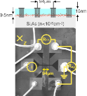
Our test device was grown by saturation-dosing of PH3 on a Si(100) flat surface, annealing for 2 minutes at 350 C, then overgrowing 15 nm of silicon at 250 C without the use of a locking layerHagmann:2018ul ; Keizer:2015fk . This is similar to the work by Goh et al.Goh:2006ye . The finished -layer was processed into Hall bars, with mesa dimensions 9420 . Scanning tunnelling microscopy (STM) measurements yielded a nominal sheet density of 21014 cm-2, and the measured Hall sheet density was 2.81014 cm-2 in the temperature range measured. The device was mounted in a dilution refrigerator with a 3D vector magnet capable of a field magnitude of 2 T in all directions. The base temperature was 13 mK (22 mK with the field sweeping). Transverse and longitudinal resistance were measured for linear field sweeps, with the magnetic field out of plane (), in plane ( and ), and for angular sweeps at a field magnitude of 2 T in all three planes. The temperature was varied from 22 mK to 30 K. Additionally, angular sweeps were performed at 22 mK with different field magnitudes, from 2 T to 0.1 T. The current in all magnetoresistance (MR) measurements was 114 nA. The current modulation frequency in all measurements was 7.6 Hz. The main axes of the magnetic field were finely adjusted by applying a maximum in-plane field in the X and Y directions and minimizing the hall effect. An optical image and cross section of the sample appear in Figure 1.
III Results
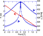
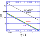
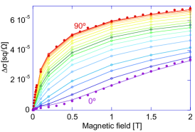
Figure 1 shows magnetotransport (MT) curves with the field out of plane (transverse and longitudinal MR) and in plane (longitudinal MR). The fitted longitudinal MT is according to Hikami et al. Hikami:1980vn and Dugaev and Khemlnitskii Dugaev:1985fv . The resulting layer thickness following Sullivan et al.Sullivan:2004lr is nm, with a negligible temperature dependence. There was no measurable difference between the MR with the field in both in-plane directions. Figure 1 shows the temperature dependence of the transport parameters derived from the fits. We see that the conductivity scales as , as expected Altshuler:1980hh . The phase coherence length has a strong temperature dependence, and much like previous results in different material systems and thicknesses it saturates at low temperaturePolley:2011ly ; Cheung:1994mk ; Fournier:2000qq ; Ihn:2008hp ; Ki:2008ye ; Lin:2002rm . We do not take this as an indication that the actual sample temperature saturates, since the magnitude of the zero-field peak caused by the superconducting transition of the aluminum contacts Polley:2011ly ; Caplan:1965fk is still temperature-dependent at these low temperatures. The mean free path is only weakly temperature dependent, and as the temperature increases tends towards . We expect the WL approximation to break down as a result. The experimental values of are shown in Figure 1 and we find that they are proportional to as expected, with a weak temperature dependenceMensz:1987fk . The proportionality coefficient is orders of magnitude lower than in previous MOSFET results, meaning that the in-plane field in our work has a larger phase-breaking effect. We attribute this to a rougher interface of the -layer compared with the MOSFETMensz:1987uq .
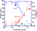
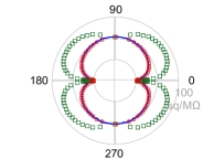
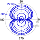
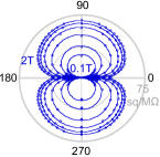
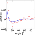
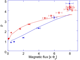
Figure 2 shows (hereafter referred to as ) at 22 mK and 2 T as a function of the field angle in the ZX plane (blue). The sum of caused by a parallel field and a perpendicular field at the appropriate magnitudes is shown in green. The traces intersect at 0∘, 90∘, 180∘ and 270∘ (measured from the plane), since only one field component is nonzero. At other angles this is clearly not the case. The red trace is a -mean of the perpendicular and parallel field MC, where the fitted value of is . The -mean fits at a temperature range of 22 mK – 30 K are shown in Figure 2; the quality of the fits remain good, and decreases as the temperature rises. and -mean fits at 22 mK, for different field magnitudes, are shown in Figure 2, and we see that increases with the magnitude of the field. Figure 2 shows that the normalized deviation between the tilted-field measurement and the -mean fit remains within 5%. The symbols in Figure 3 are the experimental -values, obtained from Figures 2 and 2, as a function of the number of magnetic flux quanta through the maximal area enclosed before dephasing, i.e. . Separate sets of points are shown for measurements where the field is varied (blue) and where was varied by changing the temperature (red).
l-1ptb-2pt
l0ptb-2pt
l23ptt1pt
IV Discussion
To understand the origin of the -mean we begin by considering the isotropic 3D case, where the MC depends only on the magnitude of Kawabata:1980fk ; Kawabata:1980kx ; Yamanouchi:1967rm ; Rosenbaum:1981fv . At low and high fields it can be approximated by a local power law
| (3) |
where , respectively. For intermediate fields the relation also holds for and a which depends on the field , so that the degree of non-linearity of the MC is encoded in . Let be the angle between the field and an arbitrarily chosen plane in an isotropic sample, so and ; then by using Equation 3 the -mean relation holds identically:
A corresponding theory for anisotropic 3D samples, where depends also on the angle of the field w.r.t. a reference plane in the sample, was discussed by Mauz et al. Mauz:1997fb . A one-parameter scaling rule for the magnetic field was deduced by which for all angles collapses onto a single scaling curve:
| (5) |
where the anisotropy enters only through the effective field , related to the physical field by the angle-dependent scale factor . determines the effectiveness of a field at angle in disrupting WL relative to that of a perpendicular field.
Following [Mauz:1997fb, ] we define a scaling for our single quasi-two-dimensional layer as
| (6) |
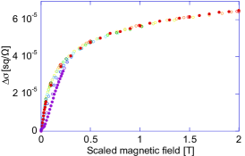
where denotes the effective anisotropy ratio, which can be approximately taken as constant over the angle and field ranges in the experiment (see Supplementary). We find a similar scaling collapse in our experimental data, as shown in Figure 4: MC curves taken at a full range of angles collapse onto the perpendicular field MC, which is well fitted by the expression derived in [Hikami:1980vn, ]. The temperature dependence of appears in the inset, showing that the system becomes more isotropic as the temperature increases. We have also found that to a good approximation this same scaling collapse is empirically obeyed in Mathur’s theory for a single layer with finite layer roughness and finite temperature Mathur:2001fr . For large angles we see
| (7) | |||||
We see that if is taken to be the log-derivative of then
Additionally, if were a power-law (Eq. 3) then it would follow that
In that case the p-mean relation (Equation 2) would hold as a result of scaling and power-law dependencies. Interestingly we find that even though does not follow a power-law dependence, the empirical value of is modified such that the -mean rule still applies and we can regard as describing the interplay between and the vector field in the 2D case.
r3ptb21pt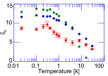
We see that, provided a local power law exists, the -mean is intrinsic to the isotropic bulk case. Furthermore, in the 2D case we successfully describe the tilted-field MC using the Hikami formula and a scaled field, and derive the -mean from that scaling. We can now make several observations regarding the power law, and . The ansatz in Equation 3 helped to demonstrate the -mean relation for strictly field-magnitude related MC. We can show that for a particular field angle this power-law relation emerges directly from our scaling and -mean observations. We define a ‘crossing angle’ where the influence of the parallel and perpendicular fields, applied separately, is equal: , where
| (8) |
At this angle the -mean exponent can be conveniently expressed as
| (9) |
provided Equation 2 holds at the crossing point (which is empirically found to be the case, see Figure 2). At the crossing angle we have, using Equation (5),
| (10) | |||||
and hence
| (11) |
i.e. the easily-measurable directly quantifies the MC anisotropy.
Using Equation 6 we see that . Once again using the empirical validity of Equation 2 at the crossing point, we see that
| (12) |
This expression for does not rely on the power-law assumption of Equation 3. It then follows that
| (13) |
i.e. it emerges that encodes a power-law behavior of the MC scaling function at the crossing angle similar to Equation 3.
can be related, at high fields, to , and (the elastic, inelastic and phase-breaking times, respectively) through an asymptotic approximation, i.e. at grazing angles (see Supplementary)
| (14) |
where is the diffusion constant and is the digamma function. The values for Equation 14 appear in the inset of Figure 4 (green circles) and we find the good agreement with the fitted data to be consistent with our understanding of : a large anisotropy results in a that is close to the plane, making the asymptotic approximation in our calculation valid.
Equations 11 and 12 give a full vector-characterization of anisotropic 2D-like WL. Given the results of a perpendicular- and parallel field MC measurement (e.g. the squares and triangles in Figure 1, respectively), then the crossing angle can be found, for arbitrary magnetic fields, by interpolation. Both and can then be calculated, and using Equations 5 and 6 or 2, respectively, a full angle and field-magnitude map of is constructed.
can also give an indication to the layer thickness; a natural interpretation of the scaling collapse in Equations 5 and 6 is that the MC is determined by the magnetic flux through an angle-dependent phase-breaking area. Taking the effective phase-breaking length perpendicular to the field as , we might guess that the scaling approach would be valid until angles are reached such that the projection of becomes comparable to the layer thickness, . Thus the breakdown of scaling gives a second – independent – estimate of , which yields at 22 mK.
V Conclusions
We have taken advantage of modern vector magnet and sample preparation technologies to revisit the problem of weak localization in silicon, where we have now implemented a two-dimensional half-filled disordered Hubbard model with t/U of order unity. To the best of our knowledge, the experiments represent the first attempt to examine the entire temperature and vector field dependence of the conductance for the realization of such a model, and we find astonishingly precise agreement with forty year-old theory, incorporating the effects of interface roughness but neglecting Coulomb interactions. The MC in a tilted field is found to be a -mean of the MCs in the parallel and perpendicular field components separately. In analogy to the dependence of on the magnitude of in the three-dimensional case of KawabataKawabata:1980fk , we can regard as a generalised measure of the sensitivity of to the varying vector in the two-dimensional case.
There is a scaling collapse of the MC onto a single function of an angle-dependent effective magnetic field. Such a scaling form has previously been proposed for anisotropic 3D systems Mauz:1997fb , but it is interesting that it holds also in the almost purely two-dimensional system formed by our -layer. Scaling is well obeyed for all field directions except when the field is very nearly in-plane. At these angles a crossover occurs to a different regime dominated by the parallel field; the out-of-plane confinement dominates the response to the field and the anisotropic 3D assumption breaks down.
Supplementary information:
Dependence of the scaling parameter on
Relying on the empirical validity of the scaling ansatz for a range of fields and angles we can extract a dependence of the scaling parameter on the system parameters. The scaling ansatz enables us to obtain an expression for the vector magentoconductance in terms of the perperndicular magnetoconductance Hikami:1980vn and the scaling function
where represents the dephasing strength of the parallel magnetic field, as has been discussed in several microscopic derivations Dugaev:1985fv ; Mensz:1987fk ; Mathur:2001fr and is the rescaled effective magnetic field. We can now try to compare the magentoconductances assuming that , an assumption which yielded a good description to as described in the main text with Eq. (11). For low temperatures we find that the crossing angle is relatively small. Equating and and numerically extracting the dependence of on temperature even for very small angles yields a good approximation to the dependences depicted in the inset of Figure 4(b).
In order to obtain insight into the dependence of on the physical parameters we proceed with approximating each of the Digamma functions which appear above in the expressions for and . For small angles and the values of relevant for Figure 4(b), can be expanded close to i.e. where
whereas the other Digamma functions are approximated by an asymptotically as logarithms since they possess large numerical arguments.
where we find that it is sufficient to take the zero’th order approximation in the Taylor expansion for the last term. By equating and and extracting we immediately obtain
which can also be expressed in terms of the microscopic relaxation times as
| (15) |
This expression reveals the dependence of the scaling parameter on the microscopic parameters and strengthens our assertion that the anisotropy of the system is highest at low temperature. This dependence is plotted in Figure 4(b) and while it works well to qualitatively describe the dependence for a large range of temperatures it is understandably less accurate for high temperature where the crossing angles are large.
We note that according to this derivation also observes a dependence on the magnetic field. We argue that this manifests the approximate nature of the scaling ansatz where is taken constant. The constant is determined by a fit and is mostly influenced by medium field strengths data. The reason is that influence of is most important at medium range fields because at small fields the magnetoconductance is small and at large fields the magnetoconductance varies slowly with fields. In practice this typical scaling factor, when applied to all measured angles and fields performs well. We also see that the dependence of with temperature, i.e. is consistent with trend that we find here.
References
- [1] S. R. Schofield, N. J. Curson, M. Y. Simmons, F. J. Rueß, T. Hallam, L. Oberbeck, and R. G. Clark. Atomically Precise Placement of Single Dopants in Si. Physical Review Letters, 91:136104, 2003.
- [2] Giordano Scappucci, Wolfgang M. Klesse, LaReine A. Yeoh, Damien J. Carter, Oliver Warschkow, Nigel A. Marks, David L. Jaeger, Giovanni Capellini, Michelle Y. Simmons, and Alexander R. Hamilton. Bottom-up assembly of metallic germanium. Scientific Reports, 5:12948, 08 2015.
- [3] Herng‐Der Chiou. Phosphorus Concentration Limitation in Czochralski Silicon Crystals. Journal of The Electrochemical Society, 147(1):345–349, 2000.
- [4] S. R. McKibbin, C. M. Polley, G. Scappucci, J. G. Keizer, and M. Y. Simmons. Low resistivity, super-saturation phosphorus-in-silicon monolayer doping. Applied Physics Letters, 104(12):123502, 2014.
- [5] S. Solmi, A. Parisini, R. Angelucci, A. Armigliato, D. Nobili, and L. Moro. Dopant and carrier concentration in Si in equilibrium with monoclinic SiP precipitates. Physical Review B, 53:7836–7841, March 1996.
- [6] R. G. Wheeler. Magnetoconductance and weak localization in silicon inversion layers. Physical Review B, 24:4645–4651, October 1981.
- [7] M.Y. Simmons, A.R. Hamilton, M. Pepper, E.H. Linfield, P.D. Rose, and D.A. Ritchie. Metallic behaviour and localisation in 2D GaAs hole systems. Physica E: Low-dimensional Systems and Nanostructures, 11(2–3):161–166, 2001. Proceedings of the Rutherford Memorial Workshop on Semiconductor Nanostructures, Qeenstown, New Zealand, 5-9 February 2001.
- [8] Samuel Lara-Avila, Alexander Tzalenchuk, Sergey Kubatkin, Rositza Yakimova, T. J. B. M. Janssen, Karin Cedergren, Tobias Bergsten, and Vladimir Fal’ko. Disordered Fermi Liquid in Epitaxial Graphene from Quantum Transport Measurements. Physical Review Letters, 107:166602, October 2011.
- [9] A. L. Saraiva, A. Baena, M. J. Calderón, and B. Koiller. Theory of one and two donors in silicon. Journal of Physics: Condensed Matter, 27(15):154208, 2015.
- [10] Nguyen H. Le, Andrew J. Fisher, and Eran Ginossar. Extended hubbard model for mesoscopic transport in donor arrays in silicon. Phys. Rev. B, 96:245406, Dec 2017.
- [11] Antoine Georges, Gabriel Kotliar, Werner Krauth, and Marcelo J. Rozenberg. Dynamical mean-field theory of strongly correlated fermion systems and the limit of infinite dimensions. Rev. Mod. Phys., 68:13–125, Jan 1996.
- [12] Shinobu Hikami, Anatoly I. Larkin, and Yosuke Nagaoka. Spin-orbit interaction and magnetoresistance in the two dimensional random system. Progress of Theoretical Physics, 63(2):707–710, 1980.
- [13] P. M. Mensz and R. G. Wheeler. Magnetoconductance due to parallel magnetic fields in silicon inversion layers. Physical Review B, 35:2844–2853, February 1987.
- [14] H. Mathur and Harold U. Baranger. Random Berry phase magnetoresistance as a probe of interface roughness in Si MOSFETs. Phys. Rev. B, 64:235325, Nov 2001.
- [15] Joseph A. Hagmann, Xiqiao Wang, Pradeep Namboodiri, Jonathan Wyrick, Roy Murray, M. D. StewartJr., Richard M. Silver, and Curt A. Richter. High resolution thickness measurements of ultrathin Si:P monolayers using weak localization. Applied Physics Letters, 112(4):043102, 2018.
- [16] Joris G. Keizer, Sebastian Koelling, Paul M. Koenraad, and Michelle Y. Simmons. Suppressing Segregation in Highly Phosphorus Doped Silicon Monolayers. ACS Nano, 9(12):12537–12541, 12 2015.
- [17] K. E. J. Goh, L. Oberbeck, M. Y. Simmons, A. R. Hamilton, and M. J. Butcher. Influence of doping density on electronic transport in degenerate Si:P -doped layers. Physical Review B, 73:035401, January 2006.
- [18] V. K. Dugaev and D. E. Khemlnitskii. Magnetoresistance of metal films with low impurity concentrations in a parallel magnetic field. Soviet Physics Journal of Experimental and Theoretical Physics, 59:1038, 1985.
- [19] D. F. Sullivan, B. E. Kane, and P. E Thompson. Weak localization thickness measurements of Si:P delta-layers. Applied Physics Letters, 85(26):6362–6364, 2004.
- [20] B. L. Altshuler, D. Khmel’nitzkii, A. I. Larkin, and P. A. Lee. Magnetoresistance and Hall effect in a disordered two-dimensional electron gas. Physical Review B, 22:5142–5153, December 1980.
- [21] Craig M. Polley, Warrick R. Clarke, and Michelle Y Simmons. Comparison of nickel silicide and aluminium ohmic contact metallizations for low-temperature quantum transport measurements. Nanoscale Research Letters, 6:538, October 2011.
- [22] R. Cheung, L.J. Geerligs, J. Caro, A.H. Verbruggen, K. Werner, and S. Radelaar. Weak localisation and correlation effects in a two dimensional hole gas in Si/Si1−xGex heterostructures. Physica B: Condensed Matter, 194:1225–1226, 1994.
- [23] P. Fournier, C.J. Lobb, and R.L. Greene. Saturation of the phase coherence length at low temperatures in Pr1.95Ce0.05CuO4. Physica C: Superconductivity, 341:1941–1942, 2000.
- [24] T. Ihn, D. Graf, F. Molitor, C. Stampfer, and K. Ensslin. Phase-coherent transport in a mesoscopic few-layer graphite wire. Physica E: Low-dimensional Systems and Nanostructures, 40(6):1851–1854, 2008. 13th International Conference on Modulated Semiconductor Structures.
- [25] Dong-Keun Ki, Dongchan Jeong, Jae-Hyun Choi, Hu-Jong Lee, and Kee-Su Park. Inelastic scattering in a monolayer graphene sheet: A weak-localization study. Physical Review B, 78:125409, September 2008.
- [26] J. J. Lin, Y. L. Zhong, and T. J. Li. Effect of annealing on electron dephasing in three-dimensional polycrystalline metals. Europhysics Letters, 57(6):872, 2002.
- [27] Sandor Caplan and Gerald Chanin. Critical-Field Study of Superconducting Aluminum. Physical Review, 138:A1428–A1433, May 1965.
- [28] P. M. Mensz, R. G. Wheeler, C. T. Foxon, and J. J. Harris. Determination of spatial potential fluctuations in si and gaas inversion layers by weak localization. Applied Physics Letters, 50(10):603–605, 1987.
- [29] A. Kawabata. Theory of negative magnetoresistance in three-dimensional systems. Solid State Communications, 34(6):431–432, 1980.
- [30] Arisato Kawabata. Theory of negative magnetoresistance i. application to heavily doped semiconductors. Journal of the Physical Society of Japan, 49(2):628–637, 1980.
- [31] Chikako Yamanouchi, Kanji Mizuguchi, and Wataru Sasaki. Electric Conduction in Phosphorus Doped Silicon at Low Temperatures. Journal of the Physical Society of Japan, 22(3):859–864, 1967.
- [32] T. F. Rosenbaum, R. F. Milligan, G. A. Thomas, P. A. Lee, T. V. Ramakrishnan, R. N. Bhatt, K. DeConde, H. Hess, and T. Perry. Low-Temperature Magnetoresistance of a Disordered Metal. Physical Review Letters, 47:1758–1761, Dec 1981.
- [33] C. Mauz, A. Rosch, and P. Wölfle. Dimensional crossover of weak localization in a magnetic field. Physical Review B, 56:10953–10962, November 1997.