Pathway towards programmable wave anisotropy in cellular metamaterials
University of Minnesota, Minneapolis, MN 55455, USA
∗sgonella@umn.edu
Published article: Phys. Rev. Appl. 9 (1), 014014 (2018)
https://doi.org/10.1103/PhysRevApplied.9.014014 )
In this work, we provide a proof-of-concept experimental demonstration of the wave control capabilities of cellular metamaterials endowed with populations of tunable electromechanical resonators. Each independently tunable resonator comprises a piezoelectric patch and a resistor-inductor shunt, and its resonant frequency can be seamlessly re-programmed without interfering with the cellular structure’s default properties. We show that, by strategically placing the resonators in the lattice domain and by deliberately activating only selected subsets of them, chosen to conform to the directional features of the beamed wave response, it is possible to override the inherent wave anisotropy of the cellular medium. The outcome is the establishment of tunable spatial patterns of energy distillation resulting in a non-symmetric correction of the wavefields.
INTRODUCTION
Cellular solids are porous media known to display unique combinations of complementary mechanical properties, such as high stiffness and high strength at low densities [1]. Lattice materials—cellular solids with ordered architectures—are obtained by spatially tessellating a fundamental building block (unit cell) comprising simple slender structural elements such as beams, plates or shells. Advances in additive manufacturing have recently propelled a resurgence of architected cellular solids as mechanical metamaterials with unprecedented functionalities at multiple scales [2, 3, 4, 5]. Examples include fully-recoverable, energy absorbing lattices with bucklable struts [6, 7], pentamode fluid-like materials that behave as “unfeelability” cloaks [8], lattices with negative Poisson’s ratio [9], negative thermal expansion [10], and smart lattices with programmable stiffness [11].
Lattice structures also display unique dynamic properties. They commonly feature Bragg-type bandgaps as a result of their periodicity and occasionally subwavelength bandgaps for special unit cell designs or in the presence of internal resonators, thus behaving as frequency-selective stop-band filters for acoustic [12], elastic [13, 14, 15, 16, 17, 18, 19] and electromagnetic waves [20]. They also display elastic wave anisotropy, which manifests as pronounced beaming of the energy according to highly directional patterns [21, 22, 13, 23, 24, 25, 26, 27, 28, 29, 30]. This behavior can be attributed to the fact that, at the cell scale, elastic waves are forced to propagate along the often tortuous pathways dictated by the links/struts. The spatial characteristics, symmetry landscape and frequency dependence of the anisotropic patterns are dictated by the unit cell’s architecture [31, 32] and are usually irreversibly determined during the design and fabrication stages. To endow cellular solids with functional flexibility and active spatial wave management capabilities, we need our structural systems to be tunable or programmable [33, 34, 35, 36, 37, 38, 39, 40, 41, 42]. To ensure that geometry and material requirements imposed by other functional constraints are preserved during the tuning process, it is especially important to devise minimally invasive tunability strategies [43].
In this work, we propose and implement a strategy for tailorable spatial wave management in architected cellular solids, based on the interplay between the inherent anisotropy of the underlying lattice medium and the resonant behavior of tunable resonators strategically located on selected lattice links. Let us recall here that a resonator attached to a structural medium interacts with an incident propagating wave by distilling from the wave spectrum an interval of frequencies comprised within the neighborhood of its resonant frequency [44, 45]. This behavior can be explained by invoking the destructive interference mechanisms between the incident wave and the wave that the resonator re-radiates, which experiences a 180o phase shift for frequencies immediately above resonance [46]. As a result, by tuning the resonators as to induce distillation at frequencies for which the lattice displays anisotropic directional wavefields, and by activating selected spatial subsets of resonators located along the dominant energy beams of the directional fields, we can override selected spatial wave features. The result is a smart lattice structure whose spatial wavefields can be programmed to display several complementary pattern corrections that relax the symmetry of the response. For this task, we resort to resonators consisting of thin, minimally invasive piezoelectric patches shunted with resistor-inductor (RL) circuits to realize resonant RLC units, adapting and perfecting a framework previously established for beams, plates and waveguides [47, 48, 49, 50, 51, 52, 45, 53, 54]. The resonant frequency of each electromechanical resonator can be seamlessly varied by modifying the electrical impedance of the corresponding shunting circuit, which is carried out by simply tuning one of the circuit components.
EXPERIMENTAL SETUP
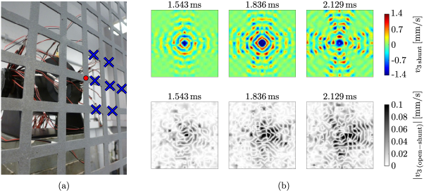
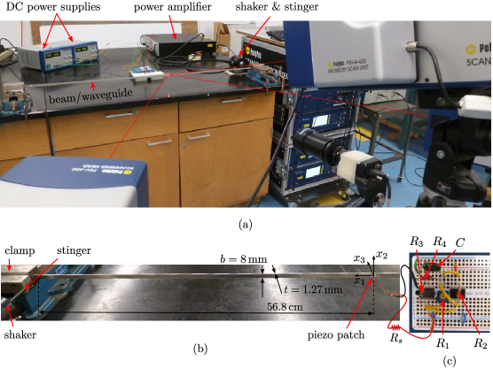
Our experimental setup is illustrated in Fig. 1a.
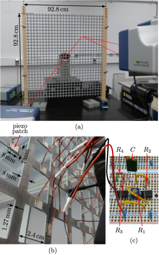
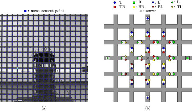
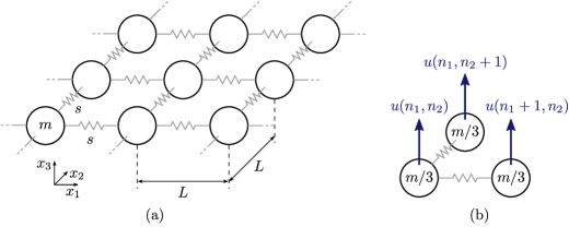
The cellular medium of choice is a square lattice specimen, comprising 2929 unit cells, manufactured out of a -thick 6061 aluminum plate (Young’s modulus , density , Poisson’s ratio ) using water jet cutting. The characteristic length of the unit cell is , and the width of a lattice link is . The out-of-plane motion of points on the front face of the specimen that correspond to a pre-determined scanning grid is measured via a 3D Scanning Laser Doppler Vibrometer (3D-SLDV). The excitation signals are imparted through an electromechanical shaker and a stinger, connected to the lattice node at the center of the specimen. A detail of the rear face of the specimen near the actuation location, shown in Fig. 1b, highlights the presence of multiple piezoelectric patches ( wafers made of PZT-5A) bonded to the structure. A total of 28 patches are located as to form a ring around the excitation point. All the patches are wired, but only up to seven (or eight) are simultaneously activated—i.e. connected to a RL circuit—during each experiment. Eight synthetic inductors (Antoniou circuits) are built on a solderable breadboard to serve as equivalent inductors for the eight required shunting circuits; one of them is shown in Fig. 2c. Synthetic inductors are a staple in the shunting literature due to their compact dimensions (even for large values of inductance), versatility and tunability [56]. DC power supplies are used to power the Op-Amps in the Antoniou circuits. To seamlessly program the synthetic inductor (and consequently the characteristics of the resonator), the resistor in each circuit is a tunable potentiometer; modifying changes the equivalent inductance and, therefore, the resonant frequency , where is the capacitance of the piezo patch. The circuit components are selected as to allow the resonators to be tuned at any frequency in the interval from to . Series resistors are required to introduce enough damping to alleviate the effects of circuit instabilities [57]. More details on the experimental setup, on the circuits and on their tuning are reported in the Supplemental Material [55].
NUMERICAL AND EXPERIMENTAL WAVE RESPONSE
The default wave response of the pristine lattice is illustrated in Fig. 2.
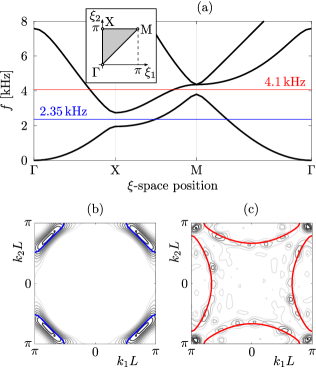
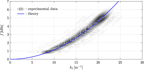
The band diagram of an infinite lattice having the same cell dimensions, geometry and material properties as our specimen is shown in Fig. 2a; this result is obtained through a Bloch analysis of a unit cell modeled with plate finite elements (implementing Mindlin’s plate model) limited to wave vectors sampled along the contour of the Irreducible Brillouin Zone (IBZ) [13]. We are especially interested in frequencies where the appearance of partial bandgaps suggests pronounced wave anisotropy. In the low-frequency range shown in Fig. 2a, these frequencies are approximately and . The blue lines in Fig. 2b mark the Cartesian iso-frequency contour obtained by slicing the first dispersion surface at , and highlight how, at this frequency, waves are predominantly allowed to propagate along directions that are -oriented with respect to the horizontal axis. Iso-frequency contours provide information analogous to the slowness curves [58], whereby proximity to the origin implies high phase velocity, and vice versa. The iso-frequency contour of the second surface at displays complementary features: wave speeds are now much higher along the horizontal and vertical directions.
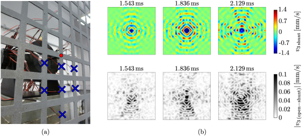
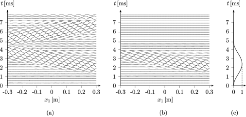
In Fig. 3, we report the out-of-plane velocity snapshots (at two time instants) of the measured transient response of our lattice specimen. The excitation signals are 13-cycle bursts with carrier frequencies corresponding to and , respectively. Note that, at this stage, all patches are in their open circuit configuration.
The response at (Fig. 3a) shows that, at this frequency, the wavefields feature four highly-beamed packets propagating along -oriented directions, as predicted by the iso-frequency contour in Fig. 2b. On the other hand, the wavefields corresponding to (Fig. 3b) feature packets propagating mainly along the vertical and horizontal directions—consistent with the predictions of Fig. 2c. In Figs. 2b-c, to further demonstrate the excellent agreement between the results from the unit cell analysis and the laser-acquired experimental data, we superimpose to the iso-frequency contours the spectral lines of the lattice response at the same frequencies, obtained from the experimentally acquired wavefields through a 2D Discrete Fourier Transform procedure (2D-DFT; see the SM section for details on the reconstruction procedure). This comparison also highlights how the presence of the open circuit (non-shunted) patches has minimal influence on the characteristics of the medium in this low-frequency regime.
WAVE-RESONATOR INTERACTION
To elucidate the mechanisms behind the wave-resonator interaction in the specific case where the resonator comprises a piezoelectric patch shunted with a RL circuit, we resort to a simple one dimensional experiment. The specimen is a -long and -wide beam with the same thickness and material properties as the lattice specimen. The beam is clamped at both ends, and the excitation is imparted near one of the clamps. Approximately at the center of the beam, we bond a single piezoelectric patch (identical to those used in the lattice experiment). A schematic of the beam, with illustration of the location where the response is measured by the 3D-SLDV system, is shown in Fig. 4a (the setup for this experiment is shown in Fig. S7 and discussed in the Supplemental Material [55]).
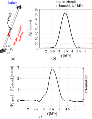
The beam is excited via a 9-cycle burst with carrier frequency . Boundary reflections are eliminated through a time-filtering procedure, also discussed in [55]. In Fig. 4b, we compare the frequency spectra of the out-of-plane velocity signals recorded in the open circuit case (gray line) and in the shunted case (black line). These signals have been obtained by averaging the response at multiple measurement points located after the resonator. The patch-circuit system is tuned as to resonate around , although a small error in pinpointing the frequency is often expected. We observe that, as predicted, the resonator causes wave attenuation/distillation in the neighborhood of the tuning frequency. The amplitude of attenuation is small compared to other instances reported in the literature on shunted systems due to the fact that here the wave packet is purely incident and interacts with the resonator only once. Stronger attenuation results usually arise from multiple wave-resonator interactions, as in steady-state conditions or when we can aggregate the effects of multiple transient packets bouncing back and forth between the structure’s boundaries [45]. The action of the resonator can be better visualized by subtracting the shunted spectrum from the open circuit one; this differential plot is shown in Fig. 4c. Notably, most of the attenuation is recorded right above the expected resonance. This behavior can be qualitatively explained using arguments of phase delay and wave interference. Specifically, when a propagating wave interacts with a resonator, a fraction of the energy is stored in the resonator and re-radiated into the structure, possibly with a phase shift. This wave can interact constructively or destructively with the incident wave, according to their relative phase [44, 46, 59]; above resonance, where incident and re-radiated wave are in opposition of phase, destructive interference mechanisms result in signal attenuation. This effect becomes less pronounced as we move away from resonance, the resonator becomes progressively less engaged and the portion of the reradiated energy drops, ultimately dictating the width of the bandgap. Note that, while this effect is precisely observed for continuous harmonic excitation (which explains why the onset of resonant bandgaps in the frequency domain can be pinpointed experimentally with great accuracy in steady state conditions), its signature is blurrier for burst excitations with compact support where issues of packet delay and distortion may contaminate the inference.
ANISOTROPY OVERRIDING
At this stage, we know how the lattice responds to bursts at several frequencies of interest and how a traveling wave interacts with an electromechanical resonator based on a shunted piezo patch. Therefore, we have all the ingredients to investigate the influence of strategically placed, properly tuned resonators on specific wave features of the anisotropic response of the lattice. A numerical demonstration of this strategy for an idealized lattice of springs and masses with mass-in-mass nodes, which can be seen as a purely mechanical analog of our system, is reported in the Supplemental Material [55]. Despite the pronounced modeling differences, these simulations are insightful in that they allow to freely explore the parameter space of the population of resonators far beyond the constraints of the experiments. Back to our experiments, we first consider the lattice response at , shown in Fig. 3a. Our goal is to override one of the four -oriented packets propagating from the excitation point. In our first test, we shunt eight patches located along the path of the packet propagating towards the bottom-left corner of the domain. The selected patches, located on the links highlighted by cross-shaped markers in Fig. 5a, are connected to the synthetic inductors on the circuit board through series resistors with resistance .
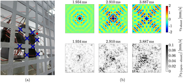
Each resonator is tuned at (see the Supplemental Material for details on the tuning procedure [55]); we choose this lower tuning frequency rather than the nominal to compensate for the shift in resonance caused by the large value of (necessary to avoid circuit instabilities). The response of the lattice at three distinct time instants is shown in the top row of Fig. 5b. At first glance, we do not detect any macroscopic modification with respect to the open circuit response of Fig. 3a. To further explore the data and reveal potential higher-order correction effects in the shunted response, in the bottom row of Fig. 5b, we report the differential wavefields obtained by subtracting the shunted response from the open circuit one at the considered time instants. Upon this operation, an asymmetric pattern consistent with our expectations unfolds. As predicted, properly-tuning a selected subset of resonators produces a frequency-distillation (and consequently an amplitude correction) of the wave packet in the spatial neighborhood of the activated resonators: packets traveling from the source towards the bottom-left corner of the domain carry the strongest signature of shunting. In Fig. 6, we report the velocity time histories recorded at four characteristic locations on the specimen’s surface—one point in each quadrant of the scanned area (top-right, bottom-right, bottom-left and top-left).
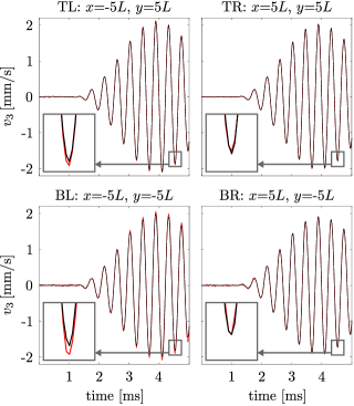
These results confirm that waves propagating towards the bottom-left corner are the most affected by the resonators and indeed experience wave attenuation. These and other results in this Section, albeit representing an unequivocal proof of concept of the anisotropy overriding capabilities of shunted lattices, reflect effects that are one order of magnitude smaller than the amplitude of the wave response. Stronger attenuation results could ostensibly be attainable through refinements of the experimental setup, e.g., by using a larger number of simultaneously activated resonators or by working with improved circuitry with reduced parasitic resistance. These technological improvements will be addressed in future investigations.
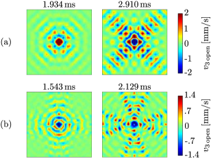
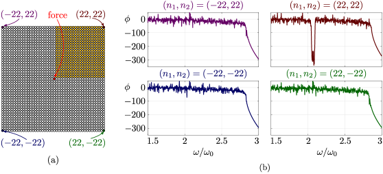
To demonstrate the tunability of our metamaterial system, we re-program the lattice by shunting a different set of patches and re-tuning the circuits as to override the wave packet propagating, still at , towards the top-left corner of the domain. Note that re-tuning is needed since each patch has a slightly different capacitance. This experiment is illustrated in Fig. 7.
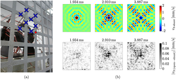
In this second scenario, we again manage to override the desired feature of the anisotropic wave pattern.
We now shift our attention towards the wave response at —characterized by complementary wave patterns propagating along the vertical and horizontal directions as illustrated in Fig. 3b. By shunting seven patches located on the links immediately to the right of the excitation point as indicated in Fig. 8a, we program the system to override the right-going wave packet. Note that, in this case, the resonators are tuned exactly at , since the required series resistance seems not to produce any appreciable shift in resonance frequency.
The differential wavefields in Fig. 8b show that the right-going horizontal feature is indeed the one being attenuated by the resonators. An additional result targeting another direction of propagation is reported for completeness in the Supplemental Material.
CONCLUSIONS
In this work, we have demonstrated that the frequency-selective anisotropic wave patterns intrinsically established in cellular metamaterials can be corrected by resorting to clouds of strategically placed, tunable electromechanical resonators and by selecting objective-specific spatial activation strategies. We have shown that we can achieve levels of programmability that allow to override the anisotropy of the wave response along different directions and at different frequencies. It is reasonable to assume that results similar to those shown in this proof-of-concept study for a simple square lattice would be achievable in more complex two- and three-dimensional architected cellular solids, albeit requiring even more complex electromechanical control systems. Integrated manufacturing of the electromechanical resonators, improved circuitry [60], or the adoption of less invasive resonators capable of offering a stronger coupling while simultaneously allowing the activation of more than seven or eight resonators could increase the tangibility of the observed effects. This kind of developments will eventually pave the way towards families of smart lattices with programmable spatial wave control capabilities such as wave steering, energy channeling and re-routing, and spatial filtering.
ACKNOWLEDGEMENTS
We acknowledge the support of the National Science Foundation (grant CMMI-1266089). PC acknowledges the support of the University of Minnesota through the Doctoral Dissertation Fellowship. We also thank Davide Cardella for his contribution during the initial stages of the project.
- [1] N. A. Fleck, V. S. Deshpande, and M. F. Ashby. Micro-architectured materials: past, present and future. Proc. R. Soc. A, 466(2121):2495–2516, 2010.
- [2] T. A. Schaedler, A. J. Jacobsen, A. Torrents, A. E. Sorensen, J. Lian, J. R. Greer, L. Valdevit, and W. B. Carter. Ultralight metallic microlattices. Science, 334(6058):962–965, 2011.
- [3] X. Zheng, H. Lee, T. H. Weisgraber, M. Shusteff, J. DeOtte, E. B. Duoss, J. D. Kuntz, M. M. Biener, Q. Ge, J. A. Jackson, S. O. Kucheyev, N. X. Fang, and C. M. Spadaccini. Ultralight, ultrastiff mechanical metamaterials. Science, 344(6190):1373–1377, 2014.
- [4] L. R. Meza, A. J. Zelhofer, N. Clarke, A. J. Mateos, D. M. Kochmann, and J. R. Greer. Resilient 3d hierarchical architected metamaterials. Proc. Natl. Acad. Sci. U.S.A., 112(37):11502–11507, 2015.
- [5] C. Coulais, E. Teomy, K. de Reus, Y. Shokef, and M. van Hecke. Combinatorial design of textured mechanical metamaterials. Nature, 535:529–532, 2016.
- [6] S. Shan, S. H. Kang, J. R. Raney, P. Wang, L. Fang, F. Candido, J. A. Lewis, and K. Bertoldi. Multistable architected materials for trapping elastic strain energy. Adv. Mater., 27(29):4296–4301, 2015.
- [7] D. Restrepo, N. D. Mankame, and P. D. Zavattieri. Phase transforming cellular materials. Extreme Mech. Lett., 4:52–60, 2015.
- [8] T. Bückmann, M. Thiel, M. Kadic, R. Schittny, and M. Wegener. An elasto-mechanical unfeelability cloak made of pentamode metamaterials. Nat. Commun., 5:4130, 2014.
- [9] R. Lakes. Advances in negative poisson’s ratio materials. Adv. Mater., 5(4):293–296, 1993.
- [10] Q. Wang, J. A. Jackson, Q. Ge, J. B. Hopkins, C. M. Spadaccini, and N. X. Fang. Lightweight mechanical metamaterials with tunable negative thermal expansion. Phys. Rev. Lett., 117(17):175901, 2016.
- [11] Y. Song, P. C. Dohm, B. Haghpanah, A. Vaziri, and J. B. Hopkins. An active microarchitectured material that utilizes piezo actuators to achieve programmable properties. Adv. Eng. Mater., 18(7):1113–1117, 2016.
- [12] S. Krödel and C. Daraio. Microlattice metamaterials for tailoring ultrasonic transmission with elastoacoustic hybridization. Phys. Rev. Applied, 6(6):064005, 2016.
- [13] A. S. Phani, J. Woodhouse, and N. A. Fleck. Wave propagation in two-dimensional periodic lattices. J. Acoust. Soc. Am., 119(4):1995–2005, 2006.
- [14] E. Baravelli and M. Ruzzene. Internally resonating lattices for bandgap generation and low-frequency vibration control. J. Sound Vib., 332(25):6562–6579, 2013.
- [15] S. Krödel, T. Delpero, A. Bergamini, P. Ermanni, and D. M. Kochmann. 3d auxetic microlattices with independently controllable acoustic band gaps and quasi-static elastic moduli. Adv. Eng. Mater., 16(4):357–363, 2014.
- [16] L. Junyi and D.S. Balint. A parametric study of the mechanical and dispersion properties of cubic lattice structures. Int. J. Solids Struct., 91:55–71, 2016.
- [17] M. Miniaci, A. Krushynska, A. B. Movchan, F. Bosia, and N. M. Pugno. Spider web-inspired acoustic metamaterials. Appl. Phys. Lett., 109(7):071905, 2016.
- [18] K. H. Matlack, A. Bauhofer, S. Krödel, A. Palermo, and C. Daraio. Composite 3d-printed metastructures for low-frequency and broadband vibration absorption. Proc. Natl. Acad. Sci. U.S.A., 113(30):8386–8390, 2016.
- [19] F. Warmuth, M. Wormser, and C. Körner. Single phase 3d phononic band gap material. Sci. Rep., 7:3843, 2017.
- [20] V. F. Chernow, H. Alaeian, J. A. Dionne, and J. R. Greer. Polymer lattices as mechanically tunable 3-dimensional photonic crystals operating in the infrared. Appl. Phys. Lett., 107(10):101905, 2015.
- [21] R. S. Langley. The response of two-dimensional periodic structures to point harmonic forcing. J. Sound. Vib., 197(4):447–469, 1996.
- [22] M. Ruzzene, F. Scarpa, and F. Soranna. Wave beaming effects in two-dimensional cellular structures. Smart Mater. Struct., 12(3):363, 2003.
- [23] J. Wen, D. Yu, G. Wang, and X. Wen. Directional propagation characteristics of flexural wave in two-dimensional periodic grid-like structures. J. Phys. D: Appl. Phys., 41(13):135505, 2008.
- [24] G. Carta, M. Brun, A.B. Movchan, N.V. Movchan, and I.S. Jones. Dispersion properties of vortex-type monatomic lattices. Int. J. Solids Struct., 51(11):2213–2225, 2014.
- [25] P. Celli and S. Gonella. Laser-enabled experimental wavefield reconstruction in two-dimensional phononic crystals. J. Sound. Vib., 333(1):114–123, 2014.
- [26] Y-F. Wang, Y-S. Wang, and C. Zhang. Bandgaps and directional propagation of elastic waves in 2d square zigzag lattice structures. J. Phys. D: Appl. Phys., 47(48):485102, 2014.
- [27] G. Trainiti, J.J. Rimoli, and M. Ruzzene. Wave propagation in undulated structural lattices. Int. J. Solids Struct., 97:431–444, 2016.
- [28] A. J. Zelhofer and D. M. Kochmann. On acoustic wave beaming in two-dimensional structural lattices. Int. J. Solids Struct., 115-116:248–269, 2017.
- [29] R. Ganesh and S. Gonella. Experimental evidence of directivity-enhancing mechanisms in nonlinear lattices. Appl. Phys. Lett., 110(8):084101, 2017.
- [30] G. Lefebvre, T. Antonakakis, Y. Achaoui, R. V. Craster, S. Guenneau, and P. Sebbah. Unveiling extreme anisotropy in elastic structured media. Phys. Rev. Lett., 118(25):254302, 2017.
- [31] P. Celli and S. Gonella. Low-frequency spatial wave manipulation via phononic crystals with relaxed cell symmetry. J. Appl. Phys., 115(10):103502, 2014.
- [32] D. Krattiger, R. Khajehtourian, C. L. Bacquet, and M. I. Hussein. Anisotropic dissipation in lattice metamaterials. AIP Adv., 6(12):121802, 2016.
- [33] M. Ruzzene and A. Baz. Control of wave propagation in periodic composite rods using shape memory inserts. J. Vib. Acoust., 122(2):151–159, 2000.
- [34] S. Shan, S. H. Kang, P. Wang, C. Qu, S. Shian, E. R. Chen, and K. Bertoldi. Harnessing multiple folding mechanisms in soft periodic structures for tunable control of elastic waves. Adv. Funct. Mater., 24(31):4935–4942, 2014.
- [35] M. A. Nouh, O. J. Aldraihem, and A. Baz. Periodic metamaterial plates with smart tunable local resonators. J. Intell. Mater. Syst. Struct., 27(13):1829–1845, 2016.
- [36] R. Zhu, Y. Y. Chen, M. V. Barnhart, G. K. Hu, C. T. Sun, and G. L. Huang. Experimental study of an adaptive elastic metamaterial controlled by electric circuits. Appl. Phys. Lett., 108(1):011905, 2016.
- [37] R. Zhu, Y. Y. Chen, Y. S. Wang, G. K. Hu, and G. L. Huang. A single-phase elastic hyperbolic metamaterial with anisotropic mass density. J. Acoust. Soc. Am., 139(6):3303–3310, 2016.
- [38] C. Croënne, M. Ponge, B. Dubus, C. Granger, L. Haumesser, F. Levassort, J. O. Vasseur, A. Lordereau, M. P. Thi, and A. C. Hladky-Hennion. Tunable phononic crystals based on piezoelectric composites with 1-3 connectivity. J. Acoust. Soc. Am., 139(6):3296–3302, 2016.
- [39] Z. Wang, Q. Zhang, K. Zhang, and G. K. Hu. Tunable digital metamaterial for broadband vibration isolation at low frequency. Adv. Mater., 28(44):9857–9861, 2016.
- [40] M. Ouisse, M. Collet, and F. Scarpa. A piezo-shunted kirigami auxetic lattice for adaptive elastic wave filtering. Smart Mater. Struct., 25(11):115016, 2016.
- [41] Y. Chen, T. Li, F. Scarpa, and L. Wang. Lattice metamaterials with mechanically tunable poisson’s ratio for vibration control. Phys. Rev. Applied, 7(2):024012, 2017.
- [42] O. R. Bilal, A. Foehr, and C. Daraio. Reprogrammable phononic metasurfaces. Adv. Mater., 29(39):1700628, 2017.
- [43] P. Celli and S. Gonella. Tunable directivity in metamaterials with reconfigurable cell symmetry. Appl. Phys. Lett., 106(9):091905, 2015.
- [44] Z. Liu, X. Zhang, Y. Mao, Y. Y. Zhu, Z. Yang, C. T. Chan, and P. Sheng. Locally resonant sonic materials. Science, 289(5485):1734–1736, 2000.
- [45] D. Cardella, P. Celli, and S. Gonella. Manipulating waves by distilling frequencies: a tunable shunt-enabled rainbow trap. Smart Mater. Struct., 25(8):085017, 2016.
- [46] F. Lemoult, N. Kaina, M. Fink, and G. Lerosey. Wave propagation control at the deep subwavelength scale in metamaterials. Nat. Phys., 9(1):55–60, 2013.
- [47] N. W. Hagood and A. von Flotow. Damping of structural vibrations with piezoelectric materials and passive electrical networks. J. Sound Vib., 146(2):243–268, 1991.
- [48] F. Casadei, M. Ruzzene, L. Dozio, and K. A. Cunefare. Broadband vibration control through periodic arrays of resonant shunts: experimental investigation on plates. Smart Mater. Struct., 19(1):015002, 2010.
- [49] L. Airoldi and M. Ruzzene. Design of tunable acoustic metamaterials through periodic arrays of resonant shunted piezos. New J. Phys., 13(11):113010, 2011.
- [50] F. Casadei, T. Delpero, A. Bergamini, P. Ermanni, and M. Ruzzene. Piezoelectric resonator arrays for tunable acoustic waveguides and metamaterials. J. Appl. Phys., 112(6):064902, 2012.
- [51] A. Bergamini, T. Delpero, L. De Simoni, L. De Lillo, M. Ruzzene, and P. Ermanni. Phononic crystal with adaptive connectivity. Adv. Mater., 26(9):1343–1347, 2014.
- [52] J. Wen, S. Chen, G. Wang, D. Yu, and X. Wen. Directionality of wave propagation and attenuation in plates with resonant shunting arrays. J. Intell. Mater. Syst. Struct., 27(1):28–38, 2016.
- [53] C. Sugino, S. Leadenham, M. Ruzzene, and A. Erturk. An investigation of electroelastic bandgap formation in locally resonant piezoelectric metastructures. Smart Mater. Struct., 26(5):055029, 2017.
- [54] M. Collet, M. Ouisse, and F. Tateo. Adaptive metacomposites for vibroacoustic control applications. IEEE Sens. J., 96(7):2145–2152, 2014.
- [55] See Supplemental Material (in tail of this document) for a more detailed account on the experimental setups and for additional results. It includes Ref. [61, 62].
- [56] G. Wang, S. Chen, and J. Wen. Low-frequency locally resonant band gaps induced by arrays of resonant shunts with antoniou’s circuit: experimental investigation on beams. Smart Mater. Struct., 20(1):015026, 2011.
- [57] F. dell’Isola, C. Maurini, and M. Porfiri. Passive damping of beam vibrations through distributed electric networks and piezoelectric transducers: prototype design and experimental validation. Smart Mater. Struct., 13(2):299, 2004.
- [58] D. Tallarico, N. V. Movchan, A. B. Movchan, and D. J. Colquitt. Tilted resonators in a triangular elastic lattice: Chirality, bloch waves and negative refraction. J. Mech. Phys. Solids, 103:236–256, 2017.
- [59] Y. Jin, B. Bonello, R. P. Moiseyenko, Y. Pennec, O. Boyko, and B. Djafari-Rouhani. Pillar-type acoustic metasurface. Phys. Rev. B, 96:104311, 2017.
- [60] E. A. Flores Parra, A. Bergamini, L. Kamm, P. Zbinden, and P. Ermanni. Implementation of integrated 1d hybrid phononic crystal through miniaturized programmable virtual inductances. Smart Mater. Struct., 26(6):067001, 2017.
- [61] submission id: submit/2163362 F. A. C. Viana and V. Steffen Jr. Multimodal vibration damping through piezoelectric patches and optimal resonant shunt circuits. J. Braz. Soc. Mech. Sci. Eng., 28:293–310, 2006.
- [62] H. H. Huang, C. T. Sun, and G. L. Huang. On the negative effective mass density in acoustic metamaterials. Int. J. Eng. Sci., 47(4):610–617, 2009.
Supplemental material (SM)
ADDITIONAL DETAILS ON THE LATTICE EXPERIMENT
In this Section, we report additional details on the experimental setup used to measure the response of the square lattice. Both signal generation and acquisition are performed through a 3D Scanning Laser Doppler Vibrometer system (3D-SLDV, Polytec PSV-400-3D). The 13-cycle burst signals are generated in MATLAB by windowing (Hann window) a sinusoidal signal, and by appending a “relaxation time” (the relaxation time, whose length is 150 times the burst length, is needed to allow the lattice structure to attain an undeformed state between consecutive measurements). The frequency of the sinusoid is the carrier frequency of the burst. The signals generated by the SLDV system have an amplitude of and are amplified through a Brüel & Kjær Type Power Amplifier, whose gain is set to . The amplified signal is then transmitted to an electromechanical shaker (Brüel & Kjær Type ), that uses a stinger to impart the excitation to the center node of the specimen. In-plane and out-of-plane velocities are measured at all the locations highlighted by blue square markers in Fig. S1a.
Due to the excitation configuration, we are only interested in the out-of-plane motion of the lattice. As for the acquisition procedure, measurements are repeated multiple times (5 times when the carrier frequency of the excitation signal is at and 10 times at ) and averaged at each measurement location to eliminate noisy features from the response. As for the vibrometer channel, we select a range and DC coupling. We select a sampling frequency and sampling points; as a result, the time step is and the total acquisition time is . An internal trigger is used to make sure there is no phase lag between the time histories recorded at different scanning points.
As we already mentioned in the main article, the square lattice is cut from a -thick 6061 aluminum plate via water jet cutting. The material properties of 6061 Al are: Young’s modulus , density , Poisson’s ratio . The lattice comprises unit cells with characteristic dimension ; the width of a lattice link is . A total of 28 piezoelectric patches (STEMiNC, part number SMPL7W8T02412WL) are bonded to the lattice links in the neighborhood of the excitation location, as shown in Fig. S1b (the patches are the light gray rectangles). In this schematic, patches are labeled according to the subset(s) to which they belong. Sets T, R, B, L are used to target the upward-, rightward-, downward-, leftward- propagating wave packets of the anisotropic wavefield at , respectively. Sets TR, BR, BL, TL are used to target the packets of the anisotropic wavefield at propagating towards the top-right, bottom-right, bottom-left and top-left corners of the lattice, respectively. The patches are carefully bonded to the lattice with a 2-part epoxy glue (3M Scotch-Weld 1838 B/A).
Two wires, one per electrode, stem from each piezoelectric patch as shown in the yellow-boxed detail of Fig. S2. This multitude of wires is connected to an intermediate breadboard (boxed in red),
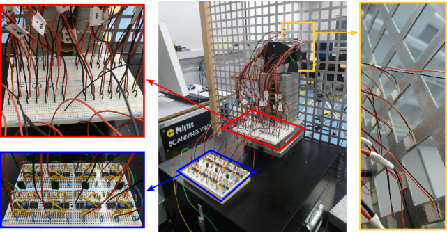
where the wires coming from the synthetic inductors (built on solderable breadboards as shown in the blue box) and from the patches are connected.
ADDITIONAL DETAILS ON THE CIRCUITRY
One of the Antoniou circuits, built on a solderable breadboard (Adafruit ADA571), is shown in Fig. S3a and schematically depicted in Fig. S3b.
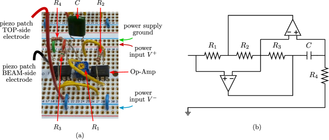
Solderable breadboards are chosen due to their improved reliability with respect to conventional ones. Each circuit comprises two operational amplifiers (TI OPA445AP), powered by two DC power supplies (BK Precision 1667) connected in series as to generate a voltage; it also comprises three conventional resistors (, , ), a potentiometer (, Copal Electronics CT6EP102-ND) and a Mylar-type capacitor (). The parameters we choose are , , , , while can be varied between and . The equivalent inductance of the Antoniou circuit is given by
| (S1) |
Given our choice of circuit parameters, can range between and . Once an Antoniou circuit is connected to a piezoelectric patch with capacitance , the resonant frequency of the patch-circuit system can be calculated as
| (S2) |
The 28 piezoelectric patches bonded to our lattice specimen do not all have the same capacitance; their average capacitance is . Using this average value and the formula in Eq. S2, we can estimate that each electromechanical resonator can be tuned between and .
To make sure that each one of the eight Antoniou circuits works properly, we test them electrically one by one before using them to shunt the piezo patches. This test is performed by connecting a synthetic inductor in series with a test resistor () and a test capacitor (, value chosen in the neighborhood of the piezo capacitance). The frequency response function of this resonant circuit, obtained in response to a multitone signal (exciting all frequencies in the – range) as the transfer function between the input voltage () and the voltage across the resistor (), is shown in Fig. S4.
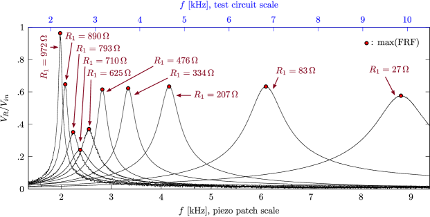
Each curve in this plot represents the response of the circuit for a specific value of . Increasing causes the resonant frequency of the circuit to decrease. This plot is characterized by two frequency scales. The original scale obtained from the experimental data is the “test circuit scale”. The other one, the “piezo patch” scale, is obtained by multiplying the frequency values of the test circuit scale by the correcting factor . The latter scale gives us an idea regarding the resonance frequency of the patch-circuit system for different values. Fig. S4 shows that for the amplitude of the resonance peak is constant and approximately equal to 0.6. For , on the other hand, the amplitude of the resonance peak is not constant; moreover, the lines corresponding to these values of are considerably more noisy, thus indicating a less stable behavior. In light of these considerations and by looking at the piezo patch scale, we can understand that resonators tuned at (the frequency corresponding to one of the two anisotropic wave patterns of interest) will be less effective than resonators tuned at (corresponding to the other anisotropic wave pattern of interest).
To tune the circuits, and to make sure that each shunt-patch system is properly tuned at the desired frequency, we are typically required to test each synthetic inductor electrically (using the same test circuit discussed above) every time we want to re-program our system. The main drawback of this electrical tuning procedure is that it heavily relies on the knowledge of the precise values of the patch capacitance [F. A. C. Viana and V. Steffen Jr, J. Braz. Soc. Mech. Sci. Eng. 28, 293 (2006)]. Moreover, since all patches have a different capacitance, it is extremely inconvenient to re-test a circuit electrically every time we want to use it to shunt a different patch. In this work, we bypass this inconvenience by exploiting the electrical instabilities that arise during the shunting process to precisely tune the electromechanical resonators. When connecting a synthetic inductor to a piezoelectric patch in the absence of a series resistor , the system is unstable, and this instability manifests as a self-excited vibration of the patch at the resonant frequency of the patch-circuit system. An audible manifestation of this instability is “screaming”—a single-pitch noise coming from the patch. Instabilities should be avoided because they are usually associated with a temperature increase that could damage the circuit components. This behavior, seldom discussed in the literature, has also been documented by dell’Isola et al. [F. dell’Isola, C. Maurini and M. Porfiri, Smart Mater. Struct. 13, 299 (2004)]. For example, the blue line in Fig. S5 represents the frequency spectrum of the signal recorded at a point of the beam when the only excitation causing it to vibrate is the self-driven instability-based vibration of the patch (no external excitation is provided). Note that the power necessary to generate these vibrations is provided by the DC power supplies that power the operational amplifiers in the synthetic inductors.
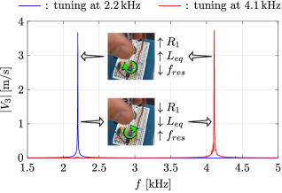
Since the peak in this frequency response corresponds precisely to the frequency at which the patch-shunt system is tuned, we can accurately tune the circuit at the desired frequency by acting on the potentiometer and by monitoring the position of this instability peak. The red line corresponds to a tuning frequency of . If we want to change the tuning frequency from to , we increase the value of (rotating the potentiometer clockwise) and, therefore, we increase while decreasing the resonant frequency of system. This way, we can move the instability peak towards lower frequencies until it is positioned at the desired value, as shown by the blue line in Fig. S5. Note that, to avoid the afore-mentioned overheating of the circuit components, it is suggested not to keep shunt and circuit connected without for more than few seconds.
When using the electromechanical resonators to control elastic waves, we need to use a large enough series resistance in the shunting circuit in order to avoid instabilities. The value of we use in the experiments at is , while the one for the experiments at is . When we target waves with carrier , we tune the circuits as to resonate at . This is done to counteract the fact that series resistors of cause a shift of the resonance peak towards higher frequencies (while no noticeable shift was noticed when tuning at ).
ISO-FREQUENCY CONTOURS RECONSTRUCTION
In Section 3 of the main article, we compared theoretical and experimentally-reconstructed iso-frequency contours, or slowness curves. The reconstruction procedure is illustrated in Fig. S6.
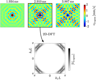
First of all, we excite the lattice structure (with all patches in their open circuit configuration) with a 13-cycle burst signal with carrier frequency . Three time instants of the out-of-plane lattice response (velocity ) are shown as wavefields in Fig. S6. We then select a time instant where the wavefield is fully developed while displays minimal boundary reflections (). Time instant , for example, is not suitable due to the fact that the wavefield is not yet well developed. On the other hand, is not suitable either due to the fact that, at this time instant, boundary reflections have started to kick in. The 2D array representing the selected wavefield data is then analyzed through the spectrum of a 2D Discrete Fourier Transform. The result of this procedure is shown at the bottom of Fig. S6; in this plot, the contours correspond to discrete values of the spectral amplitude . Since the burst excites a band of frequencies, it is impossible to reconstruct a single iso-frequency contour line. However, due to the fact that the burst is designed to give higher spectral amplitude to the carrier frequency, in this case, it is safe to assume that the experimentally-reconstructed slowness curve should go through the highest-amplitude contours. The same procedure is repeated for .
ADDITIONAL DETAILS ON THE WAVE-RESONATOR INTERACTION EXPERIMENTS
The interaction between an elastic wave and an electromechanical resonator comprising a piezoelectric patch and a resistor-inductor shunt is investigated by means of a simple one-dimensional experiment. The setup is similar to the one used to study the behavior of the lattice, and is illustrated in Fig. S7a.
The specimen is a long and wide beam carved out from the same 6061 Al sheet used to manufacture the lattice specimen (thickness ). As illustrated in Fig. S7b, a single piezoelectric patch (same as those used in the lattice experiment) is attached to the rear side of the beam, away from the point where the stinger is attached. The circuit used in this experiment is slightly different from those used in the lattice case. In particular, all circuit parameters are identical except for , which is instead of . This circuit allows to tune the resonant frequency of the electromechanical resonator from to .
The space-time evolution of a wave packet generated by a 9-cycle burst with carrier , recorded along a portion of the beam spanning to the left and to the right of the patch, is reported in Fig. S8a.
The response presents two main features. For , we can see a leftward-propagating wave traveling from the source to the opposite clamp; for , we can see a packet propagating towards the source due to boundary reflections. In order to exclude the effects of the boundary from our data and to be able to treat this as a pure propagating wave problem (i.e. lifting the possibility for standing waves to be established in the beam due to interference of incident and reflected waves), we apply the time-domain filter shown in Fig. S8c and obtain the filtered space-time data shown in Fig. S8b. Since the separation between the two packets is not very pronounced, filtering will slightly affect the signal for values of towards the left of the domain.
To evaluate the influence of the piezoelectric patch in its open circuit state on the beam response, we probe the beam with multiple 5-cycle burst signals centered at 1, 1.5, 2, 2.5, 3, 3.5, 4, 4.5, 5 and . In this case, we decided to use 5-cycle bursts to improve the separation between incident and reflected waves and to assure that the signals are not distorted by our filtering procedure. For each burst, we apply the 2D Discrete Fourier Transform to the recorded space-time data, and obtain a frequency versus wavenumber representation for the considered signal. By normalizing the response obtained for each burst and patching all the results together, we can reconstruct the dispersion relation as shown in Fig. S9.
In this plot, the experimental data is reported as contours (there are 10 sets of contours, each one for one of the excitation signals mentioned above), where the darker lines correspond to larger values of the spectral amplitude , which represents the Fourier transform of the out-of-plane velocity . This reconstructed dispersion portrait is compared to the theoretical dispersion curve for an Euler-Bernoulli beam without piezoelectric patches, i.e.
| (S3) |
where the Young’s modulus of 6061 aluminum is , its density is , the second moment of area is and the cross-sectional area is (the values given to and are those of the actual beam). The values of obtained from Eq. S3 are then normalized by , to obtain units of consistent with those obtained from the experimental data. The reconstructed and calculated dispersion relations match well, and such agreement suggests that the effect of the physical presence of the piezoelectric patch on the wave response of the beam is negligible. This strengthens the claim made in the article that the electromechanical resonators obtained by shunting the piezo patch with RL circuits are minimally invasive when the shunting circuits are open, making the all-open configuration a fair representation of the default behavior of the pristine lattice.
A NUMERICAL DEMONSTRATION OF ANISOTROPY OVERRIDING
In this Section, we provide a numerical demonstration of anisotropy overriding—the strategy for spatial wave manipulation in cellular periodic structures that we introduced in this work. The aim of this strategy is to leverage the interplay between the default anisotropically-propagating wave patterns of the cellular medium and the dynamics of resonators strategically placed at selected nodes of the lattice. Our starting point is the selection of a periodic cellular medium featuring anisotropic wave patterns at selected frequencies. We then consider a finite-size medium featuring the selected architecture and we introduce resonators in a subset of cells concentrated in certain subregion(s) of the lattice domain, in order to “override” only selected features of the anisotropic wave patterns. The main advantage of this approach is that a large number of resonators is not required to achieve significant wave focusing results.
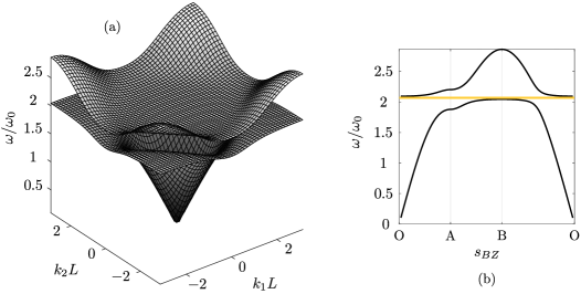
A square lattice of springs and masses
To illustrate the principles and potential of the anisotropy overriding approach, we adopt the simplest two-dimensional periodic structure—a square lattice of springs and point masses. As shown in Fig. S10a, the lattice is uniform—all springs have stiffness , all point masses have mass and are equally spaced (the inter-mass distance along both and is ).
Therefore, the position vector indicating a generic mass is , where and are integer indices. As it is extensively done in the literature, we compute the wave response of this periodic structure through a Bloch-based unit cell analysis. The unit cell used for our calculations is illustrated in Fig. S10b. Considering values of mass of instead of is necessary to obtain the exact configuration shown in Fig. S10a, upon the application of Bloch’s periodic boundary conditions. Each mass has a single out-of-plane degree of freedom, i.e. it can move vertically as illustrated by the arrows in Fig. S10b; the displacement of the mass is labeled . Hence, the springs have to be intended as constraining the vertical motion of the masses. As a result, upon application of Bloch’s conditions, the characteristic equation leads to a mono-branch dispersion relation which corresponds to a single mode of wave propagation:
| (S4) |
where is the angular frequency, while and are the Cartesian components of the wave vector. The dispersion surface for parameters is shown in Fig. S11a, where we used a normalization factor for , and for and .
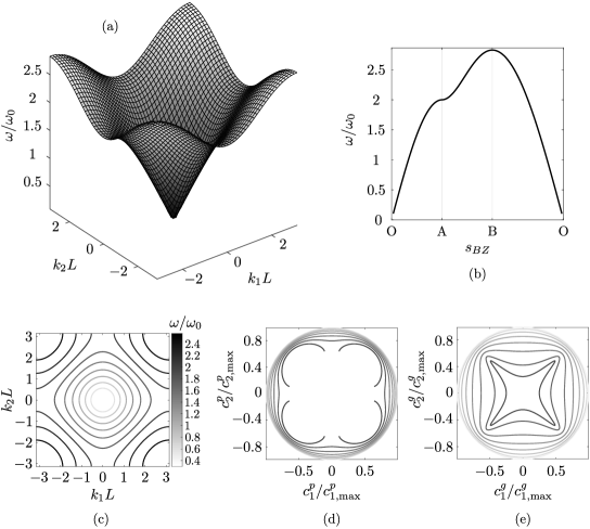
The response is more compactly represented by the band diagram in Fig. S11b, where is a coordinate spanning the contour of the IBZ of the lattice. In the reciprocal lattice coordinate system, the coordinates of the corners of the IBZ are O , A , B . As the frequency increases, we record a transition from isotropic to anisotropic wave behavior. This aspect is clearly indicated by the iso-frequency contours of the dispersion surface, shown in Fig. S11c, and by the phase and group velocity contours in Fig. S11d and Fig. S11e, respectively. This anisotropy is correlated to the arising of partial bandgaps along the and directions (denoted by the absence of points along those directions for some of the iso-frequency contours), which cause the waves to predominantly propagate along -oriented directions for frequencies greater than .
A square lattice of springs, masses and resonators
To understand the influence of localized resonators on the wave response of the spring-mass lattice introduced in the previous Section, we consider a variation of the same lattice comprising an out-of-plane spring-mass resonator for each mass. This simple model is similar in nature to the one-dimensional “mass-in-mass” one introduced by Huang et al. [H. H. Huang et al, Int. J. Eng. Sci. 47(4), 610–617 (2009)]. All resonators in the periodic lattice are characterized by stiffness and mass . The lattice is sketched in Fig. S12a, while the unit cell with all its degrees of freedom is shown in Fig. S12b.
To preserve the characteristics of the original structure, the unit cell comprises a single resonator located at the mass. Upon the application of Bloch’s conditions, the response of the infinite lattice reduces to a two degree of freedom problem. The two resulting dispersion surfaces can be computed by solving the following equation for :
| (S5) |
and by selecting only the positive roots. The dispersion surface obtained with parameters , and is shown in Fig. S13a.
The band diagram in Fig. S13b features a thin locally-resonant bandgap, highlighted in yellow, whose onset matches the resonant frequency of the resonator . The parameters of the resonator are chosen as to induce a locally resonant bandgap in a frequency region where the response of the lattice without resonators is strongly anisotropic (recall that, from Fig. S11, anisotropy is observed above ). This choice is motivated by the fact that we want our resonators to interact with the anisotropic wave patterns inherent to the baseline architecture without resonators.
Anisotropy overriding: partial bandgaps through strategically-located resonators
We now have all the ingredients necessary to introduce our spatial wave manipulation strategy, which is inherently applicable only to finite-sized structures. To do so, we consider an array of 4545 masses and we place resonators on selected masses. Throughout this analysis, the excitation is always applied at the center of the lattice, i.e., at the point corresponding to , while the response is sensed at the four corners of the lattice, i.e. at , , and . These characteristic points are color coded in the sketch of the lattice in Fig. S14a. In this sketch, and in the following ones in this Section, the yellow masses feature resonators while the white ones do not.
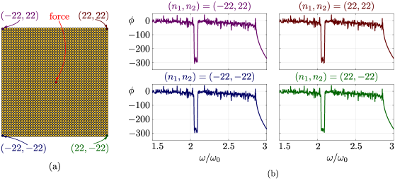
Fig. S14b represents the steady state response of the lattice with omnipresent resonators shown in Fig. S14a. The response is given in terms of transmissibilities obtained by normalizing the displacement recorded at the four corners of the lattice by the displacement of the excitation point. As expected, all four corners display a bandgap in their transmissibility; this attenuation region matches the one observed in the unit cell analysis of the same configuration (Fig. S13b). Note that the cut-off observed at , which is consistent with the absence of modes above that frequency in the dispersion relation, is due to the discrete nature of our model (which has a finite number of degrees of freedom). In Fig. S15, on the other hand, we report the response of a lattice where the only masses featuring resonators (yellow masses in Fig. S15a) are located in the top-right quadrant.
As shown in Fig. S15b, this modification of the lattice causes the appearance of a partial bandgap along the direction connecting the excitation point to the mass, while the responses along the other directions are not significantly affected by the presence of the resonators. Clearly, placing resonators in other sub-regions would produce partial bandgaps along other directions.
Our strategy relies on the mutual interaction between the inherent anisotropy of the response of a periodic medium and the partial bandgaps generated by strategically placing resonators as in Fig. S15. To harness the strongest anisotropy, we excite the lattice with a burst signal with carrier frequency . To maximize the influence of the resonators on the transient wave, and recalling that the onset of a locally-resonant bandgap coincides with the resonators’ natural frequency, we tune them at the carrier frequency of the burst. Recall, from Fig. S11, that this frequency corresponds to a propagation pattern with beaming along -oriented directions for a lattice without resonators. The response of a 4545 pristine lattice, shown in Fig. S16a, to a signal whose time evolution and frequency spectrum are shown in Fig. S16b, is reported in Figs. S16c-d.
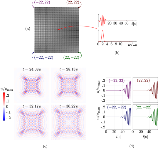
The wavefields show an “x-shaped” response that is consistent with the unit cell analysis prediction, and their main feature is represented by four spatially confined packets propagating along the -oriented directions. Our goal is to remove one (or multiple) of these packets through the introduction of resonators and the activation of partial bandgaps. An example of the application of this strategy is shown in Fig. S17, where all the masses in the top-right quadrant of the domain feature resonators.
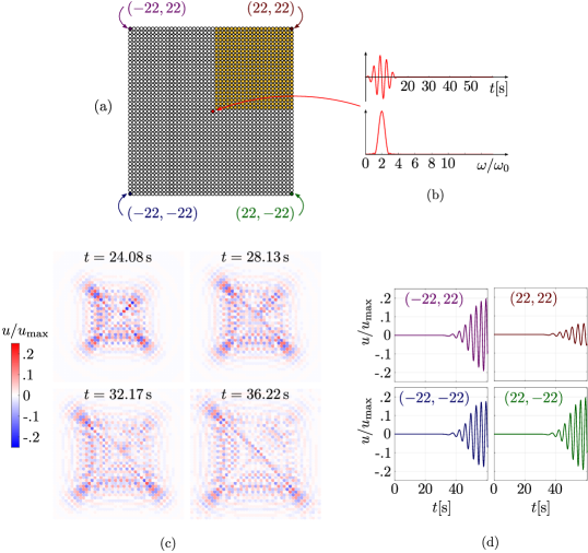
The wavefields in Fig. S17c and the time histories at the corner nodes in Fig. S17d show that, as expected, the top-right portion of the domain is significantly de-energized by the presence of the resonators. As a result, one of the four original packets is attenuated and the wave response loses its two-fold symmetry. Note that other wave focusing scenarios can be obtained by introducing resonators in other portions of the domain. It is worth pointing out that the amount of distinct wave focusing effects achievable with this strategy is symbiotic to the richness of anisotropic characteristics of the considered cellular medium. In the case of the mono-modal spring mass lattice discussed in this section, the wave focusing scenarios that can be produced are inevitably limited.
Minimizing the number of resonators
So far, we have shown the effectiveness of the anisotropy overriding strategy in the context of lattice structures where entire quadrants of the domain feature resonators. Deploying large numbers of resonators may, however, be impractical in experimental applications. With these constraints in mind, we are now interested in understanding how the number of resonators impacts the achievable symmetry modification of the anisotropic patterns, thus determining some lower bounds that can be valuable in designing effective—yet parsimonious—wave control strategies. To carry out this parametric analysis, we only introduce resonators in a square portion of the domain (with varying number of masses per side labeled by N) whose bottom left corner is fixed to the mass. Some of the considered square sub-domains are highlighted by yellow boxes in Fig. S18.
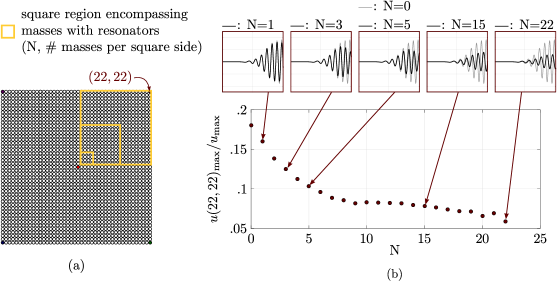
The comparison between different configurations is carried out by plotting the maximum displacement recorded at the top-right corner, (normalized by the maximum displacement recorded in the whole domain, ) against the number of masses per each side of the square subdomain featuring resonators. This trend is illustrated in Fig. S18b. For N smaller than 10, the amplitude of the displacement decreases exponentially with N, while for N greater than 10, the decrease is much less pronounced. This suggests that introducing more than 1010 resonators does not produce any significant advantage in terms of attenuation. Most importantly, the exponential nature of the first part of the curve highlights how we can obtain significant attenuation effects and therefore obtain the desired wave patterns even with a limited number of resonators.
ADDITIONAL RESULTS ON ANISOTROPY OVERRIDING
In this Section, we report one last anisotropy overriding scenario. As in Fig. 8, we consider the response to a 13-cycle burst with carrier frequency . We shunt the patches belonging to the marked links in Fig. S19a and, as shown in Fig. S19b, we alter the packet propagating downwards from the excitation location.