High Quality Factor Surface Fabry-Perot Cavity of Acoustic Waves
Abstract
Surface acoustic wave (SAW) resonators are critical components in wireless communications and many sensing applications. They have also recently emerged as subject of study in quantum acoustics at the single phonon level. Acoustic loss reduction and mode confinement are key performance factors in SAW resonators. Here we report the design and experimental realization of a high quality factor Fabry-Perot SAW resonators formed in between tapered phononic crystal mirrors patterned on a GaN-on-sapphire material platform . The fabricated SAW resonators are characterized by both electrical network analyzer and optical heterodyne vibrometer. We observed standing Rayleigh wave inside the cavity, with an intrinsic quality factor exceeding at ambient conditions.
I Introduction
In last decades, surface acoustic wave (SAW) devices have found wide use in analog signal processing Morgan (2010); Campbell (2012), wireless communications Campbell (1998); Hashimoto (2000) and a range of sensing applications Wohltjen (1984); Länge et al. (2008). Recently, SAW based quantum acoustics have received considerable attention for their flexibility in coupling with various quantum systems, including the superconducting qubits Chu et al. (2017); Gustafsson et al. (2014), NV centers in diamond Golter et al. (2016), quantum dots Schuetz et al. (2017), and is potential for building hybrid quantum networks Schütz (2017). Despite their significance in classical and quantum information processing, achieving low loss resonator and efficient mode confinement are still challenging.
By analogy to optics, an acoustic resonator can be constructed in the form of Fabry-Perot (FP) cavity in which the SAW is bounced between two mirrors and confined in between. Unlike optics where highly reflective mirrors can be patterned from a high-refractive-index waveguiding layer, unsuspended, directly etched acoustic reflectors are often insufficient in producing high enough reflectivity to prevent coupling to bulk acoustic modes Staples et al. (1974). By shorting interdigital transducers (IDT), the SAW can be confined more gently because of the small velocity contrast between the region with and without metal cladding Chen and Haus (1985). This gentle confinement however requires a large number of IDTs and hence very large device area for high reflectivity which in turn could cause SAW suffering from the Ohmic loss of the metal, leading to limited quality factor. Recently, such FP type SAW resonators have been demonstrated in the context of quantum acoustics utilizing superocnducting electrodes, with Q reaching 0.5 million but the devices are limited to operate only at cryogenic temperatures Manenti et al. (2016).
Recently it was shown that it is feasible to confine SAW with phononic band gap structuresLiu et al. (2014); Wang et al. (2015). Challenges remain in achieving full acoustic confinement and bringing the quality factor of such acoustic resonators to the value of their suspended counter part, which is fragile and requires micromachining processing. Here we report a SAW FP cavity formed by surface patterned phononic crystal (PnC) mirrors which provide high reflectivity with a much reduced mirror length, thus enabling high-Q room temperature SAW resonators. By harnessing the engineered band gap of phononic structure Khelif and Adibi (2015); Laude (2015); Maldovan (2015); Zen et al. (2014); Benchabane et al. (2015), we design the cavity for the Rayleigh surface modes. The device is fabricated by GaN-on-sapphire material system, and the cavity modes are excited by intracavity IDTs. The microwave reflection spectrum shows very high Q resonances with predicted free spectral range (FSR) , indicating the strong confinement of SAW modes and enhanced coupling to the IDTs. In addition, the cavity acoustic field is also probed by a custom-built optical vibrometer, allowing for the identification of the confined SAW modes. The demonstrated devices pave a new direction for the study of strong phonon-matter interaction as an analogue to the cavity quantum electrodynamics Soykal et al. (2011) and the cavity optomechanics Okada et al. (2017). The demonstrated high Q resonators are also promising for sensing applications based on surface acoustic wave devices.
II Design
The acoustic FP resonators are patterned from Gallium Nitride (GaN) (0001) epitaxially grown on c-plane sapphire substrate Bruch et al. (2015). GaN is a piezoelectric material with low mechanical damping Rais-Zadeh et al. (2014). Due to its lower acoustic shear velocity than that of the sapphire substrate, the acoustic waves can be guided by the GaN layer, where an acoustic cavity can be further formed by lateral confinement through a pair of PnC acoustic mirrors, schematically shown in Fig. 1(a). IDTs are directly placed within the cavity atop the GaN layer to excite SAW. At cavity resonances, standing waves are built-up within the excitation bandwidth of the IDTs. Within the cavity, the coupling between acoustic waves and the IDTs are enhanced and therefore the number of IDT electrodes can be minimized (5 pairs are utilized in a typical device). To avoid the scattering loss to the substrate, we adapted a tapered mirror design which is first proposed in Ref. Wang et al. (2015) for achieving efficient acoustic wave transitions in the phononic crystals .
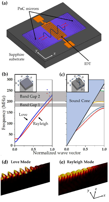
The unit cell of the PnC structure, a square pillar with a centered elliptical hole in GaN layer, is shown in the inset of Fig. 1(c), where is the period of the square lattice for both and directions, is the thickness of GaN layer, , are the major and minor radius of the elliptical hole respectively. Finite element method (FEM) simulation is performed to determine geometrical parameters of PnC unit cell using published material elastic and piezoelectric coefficientsPedrós et al. (2005). By gradully increasing the aspect ratio of elliptical PnC hole, larger phononic band gap and better comfinement of SAW can be obtained. The band structure of optimized PnC unit cell is shown in Fig. 1(c), in which the parameters are chosen to be , , , . As a comparison, the band structure for a unit cell without hole is shown in Figure 1b. The band structures are obtained by calculating the eigenmode of the PnC unit cell for different wave vectors along direction. The lightly shaded area of the band diagram represent the sound cone, in which region surface modes may coupled with bulk modes and therefore are considered to be lossy. Grey shaded areas in Figs. 1(b) and (c) indicate two phonon band gaps for wave-vectors along direction, while gap-free Rayleigh mode and Love mode are supported on flat surface without PnC structure.
The performance of PnC resonator is then analyzed with FEM simulation. Due to the relatively large transverse dimension (width) of the cavity, the resonator could be approximated to have translational symmetry along transverse () direction. Hence we only simulate one period in direction with periodical boundary condition applied. 40 periods of elliptical holes are placed on each side of cavity regime with a length of . The size of PnC holes is linearly tapered from to within 7 periods starting from the cavity mirror interface. While the simulation shows that love mode resonances are supported in both band gap 1 and band gap 2, Rayleigh mode resonances with good confinement are only found in band gap 1. At the frequency regime of band gap 2, Rayleigh wave is scattered by the PnC holes at cavity boundary, which induce a coupling between SAW and bulk mode in the sound cone, therefore prevent a strong confinement of surface mode. Hence the frequency range of band gap 1 (180 MHz to 200MHz) is chosen to design the SAW FP cavity. The modal profiles of the simulated eigenmodes are given in Figs. 1(d) and (e), including both Love modes (with mainly in-plane displacement) and Rayleigh modes (with mainly out-of-plane displacement).
III Fabrication and characterization
The device fabrication starts from the growth of GaN on c-plane sapphire wafers by metal-organic chemical vapour depositon (MOCVD) Bruch et al. (2015). To fabricate the PnC resonator, a layer of is deposited with plasma-enhanced chemical vapor deposition (PECVD). The PnC structures are patterned with electron beam lithography (EBL) using polymethyl methacrylate (PMMA) resist, followed by a lift-off process to deposit a thin layer of chromium. After liftoff, the pattern are transferred to layer by florine-based reactive ion-etching (RIE), then subsequently transferred to GaN layer by chlorine-based RIE. A second EBL process is carried on using a bi-layer PMMA resist to deposit the IDTs by a lift-off process (50nm chromium and 50nm gold).
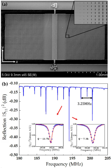
A scanning electron microscope (SEM) image of the fabricated device is shown in Fig. 2(a). The size of cavity regime is wide (in direction) and long (in direction), with a pair of PnC mirrors on the ends of cavity. Each mirror contains a square lattice PnC with elliptical holes whose dimensions are identical with the simulation. The inset shows the first eight columns of PnC holes. A chip with several fabricated devices is placed on a printed circuit board (PCB) with SMA connectors and wire bonded for the electrical characterization.
The reflection spectrum around the working frequency of the resonator is recorded with a vector network analyzer. As shown in Fig. 2(b), a series of Lorentzian-shaped dips is clearly observed, indicating a group of well confined resonance modes supported in the cavity. All modes share an approximately same free spectral range (around , as marked in the figure), suggesting that they have similar group velocities but the modes within one FSR should have different modal profiles. Based on group veolcity of Rayleigh mode (the confirmation of mode type is made through vibrometer measurement and will be discussed later) from simulation, the effective cavity length could be estimated as , which matches well with the vibrometer measurement. We attribute the resonances between each pair of main resonance dips to high-order modes along the thickness direction. They have lower extinction ratios comparing to mian resonances since the coupling between these modes and IDTs is relatively weak. Lorentzian fitting is then applied to all mode. The resonance with highest quality factor has a central frequency of , with a loaded Q of . Because all the modes are weakly coupled to the external circuit, the intrinsic Q is nearly the same with loaded Q. This quality factor is more than one order of magnitude larger than the previous work on GaN SAW resonator, while the product () is improved by a factor of three Wang et al. (2015) and becomes comparable to the suspended GaN PnC resonators Wang et al. (2014). Nevertheless, this measured is still below the theoretical prediction Rais-Zadeh et al. (2014), suggesting we have not yet reached the material limited qualty factor. The quality factor can be further improved by further reducing the radiation and the metal losses, for example, by increasing the cavity length in direction or by eliminating the radiation loss at IDT-electrode interfaces.
The resonance at , on the other hand, have the largest extinction ratio among all observed modes and is selected to analyze the coupling efficiency between IDTs and SAW. According to input-output fomula Aspelmeyer et al. (2014), the amplitude reflection of a cavity could be written as
| (1) |
where is the frequency detuning from the resonance frequency, and , are the internal and external coupling coefficient. In our case, represents the intrinsic loss in cavity (including all the losses except the loss to microwave channel), describes the coupling strength between microwave and SAW through the IDTs. The value of internal and external coupling coefficient could be extracted from the Lorentzian fitting: , . If we consider the IDTs at resonance frequency as a lumped element in transmission line, the amplitude reflection is , where is the characteristic source impedance and is the effective impedance of IDT and resonator. If and are fixed, we have . Here is found to be . Since the IDTs should be effectively considered as parallel connected component in circuit, the external coupling coefficient is propotional to the area of IDTs. By further increasing the area of IDTs, a critical coupling between microwave and acoutic cavity could be reached. In this work 5 pairs of IDT fingers are sufficient to excite SAW.
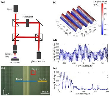
A custom-built optical heterodyne vibrometer Shen et al. (2017) is then applied to assess and identify the modal profile of the resonator. A simplified scheme of the optical heterodyne vibrometer is shown in Fig. 3(a). The mode with central frequency of with largest extinction is chosen to be the imaged. Due to the limited field of view of the vibrometer, we select three different scan locations to assess the vibration mode: a square near the center of cavity (red box in Fig. 3b), a line scan inside the cavity (blue line) and a line scan extending outside the cavity into the PnC mirror along axis (yellow line). The measurement results are shown in Figs. 3(c), (d) and (e) respectively. From Figs. 3(c) and (d), we confirm that a well confined Rayleigh mode with sinusoidal out-of-plane displacement is obtained. Love mode have not been observed under the vibrometer, due to the low excitation efficiency of IDTs for Love mode. And Fig. 3(e) shows a smooth and fast attenuation of direction displacement amplitude after the acoustic wave enters PnC regime, indicating that 100 periods of elliptical holes we use is redundant. A PnC mirror with 20 periods of PnC holes would be sufficient to confine high Q acoustic mode within the cavity, reducing the mirror length to less than .
IV Conclusion
In conclusion, we have designed and fabricated high-Q SAW Fabry-Perot resonators at the frequency around , with highest -factor about . Through vibrometer measurement, confined Rayleigh mode is directly visualized inside the cavity and evanescent wave observed at the phononic crystal mirror. Our approach can also be extended to other frequencies and may achieve even higher , particularly at cryogenic temperatures or with other materials. The demonstrated high-Q resonator is compatible with the sensing applications (such as mass sensor Luo et al. (2013) and gyroscope Jose et al. (2002)) and also is promising for the study of strong phonon-matter interaction, especially when the device is advanced to operate at tens of GHz under cryogenic condition.
Acknowledgment: We acknowledge useful discussions with M.-H. Shen. This work is supported by DARPA/MTO’s PRIGM: AIMS program through a grant from SPAWAR (N66001-16-1-4026), the Laboratory of Physical Sciences through a grant from Army Research Office (W911NF-14-1-0563), an Air Force Office of Scientific Research (AFOSR) MURI grant (FA9550-15-1- 0029) and a NSF MRSEC grant (1119826). H.X.T. acknowledges support from a Packard Fellowship in Science and Engineering. The authors thankand Dr. Michael Rooks, Michael Power, James Agresta, and Christopher Tillinghast for assistance in device fabrication.
References
- Morgan (2010) D. Morgan, Surface acoustic wave filters: With applications to electronic communications and signal processing (Academic Press, 2010).
- Campbell (2012) C. Campbell, Surface acoustic wave devices and their signal processing applications (Elsevier, 2012).
- Campbell (1998) C. Campbell, Surface acoustic wave devices for mobile and wireless communications (Academic press, 1998).
- Hashimoto (2000) K.-y. Hashimoto, Surface acoustic wave devices in telecommunications (Springer, 2000).
- Wohltjen (1984) H. Wohltjen, Sens. Actuators 5, 307 (1984).
- Länge et al. (2008) K. Länge, B. E. Rapp, and M. Rapp, Anal. Bioanal. Chem. 391, 1509 (2008).
- Chu et al. (2017) Y. Chu, P. Kharel, W. H. Renninger, L. D. Burkhart, L. Frunzio, P. T. Rakich, and R. J. Schoelkopf, Science (2017), 10.1126/science.aao1511.
- Gustafsson et al. (2014) M. V. Gustafsson, T. Aref, A. F. Kockum, M. K. Ekström, G. Johansson, and P. Delsing, Science 346, 207 (2014).
- Golter et al. (2016) D. A. Golter, T. Oo, M. Amezcua, I. Lekavicius, K. A. Stewart, and H. Wang, Phys. Rev. X 6, 041060 (2016).
- Schuetz et al. (2017) M. J. Schuetz, J. Knörzer, G. Giedke, L. M. Vandersypen, M. D. Lukin, and J. I. Cirac, arXiv preprint arXiv:1705.04860 (2017).
- Schütz (2017) M. J. A. Schütz, “Universal quantum transducers based on surface acoustic waves,” in Quantum Dots for Quantum Information Processing: Controlling and Exploiting the Quantum Dot Environment (Springer International Publishing, Cham, 2017) pp. 143–196.
- Staples et al. (1974) E. Staples, J. Schoenwald, R. Rosenfeld, and C. Hartmann, in 1974 Ultrasonics Symposium (IEEE, 1974) pp. 245–252.
- Chen and Haus (1985) D.-P. Chen and H. A. Haus, IEEE Trans. Sonics Ultrason 32, 395 (1985).
- Manenti et al. (2016) R. Manenti, M. J. Peterer, A. Nersisyan, E. B. Magnusson, A. Patterson, and P. J. Leek, Phys. Rev. B 93, 041411 (2016).
- Liu et al. (2014) T.-W. Liu, Y.-C. Tsai, Y.-C. Lin, T. Ono, S. Tanaka, and T.-T. Wu, AIP Adv. 4, 124201 (2014).
- Wang et al. (2015) S. Wang, L. C. Popa, and D. Weinstein, in 2015 28th IEEE International Conference on Micro Electro Mechanical Systems (MEMS) (2015) pp. 1028–1031.
- Khelif and Adibi (2015) A. Khelif and A. Adibi, Phononic Crystals: Fundamentals and Applications (Springer, 2015).
- Laude (2015) V. Laude, Phononic crystals: artificial crystals for sonic, acoustic, and elastic waves, Vol. 26 (Walter de Gruyter GmbH & Co KG, 2015).
- Maldovan (2015) M. Maldovan, Nat. Mater. 14, 667 (2015).
- Zen et al. (2014) N. Zen, T. A. Puurtinen, T. J. Isotalo, S. Chaudhuri, and I. J. Maasilta, Nat. Commun. 5, 3435 (2014), article.
- Benchabane et al. (2015) S. Benchabane, O. Gaiffe, R. Salut, G. Ulliac, V. Laude, and K. Kokkonen, Appl. Phys. Lett. 106, 081903 (2015).
- Soykal et al. (2011) O. O. Soykal, R. Ruskov, and C. Tahan, Phys. Rev. Lett. 107, 235502 (2011).
- Okada et al. (2017) A. Okada, F. Oguro, A. Noguchi, Y. Tabuchi, R. Yamazaki, K. Usami, and Y. Nakamura, arXiv preprint arXiv:1705.04593 (2017).
- Bruch et al. (2015) A. W. Bruch, C. Xiong, B. Leung, M. Poot, J. Han, and H. X. Tang, Appl. Phys. Lett. 107, 141113 (2015).
- Rais-Zadeh et al. (2014) M. Rais-Zadeh, V. J. Gokhale, A. Ansari, M. Faucher, D. Théron, Y. Cordier, and L. Buchaillot, J. Microelectromech. Syst. 23, 1252 (2014).
- Pedrós et al. (2005) J. Pedrós, F. Calle, J. Grajal, R. J. Jiménez Riobóo, Y. Takagaki, K. H. Ploog, and Z. Bougrioua, Phys. Rev. B 72, 075306 (2005).
- Wang et al. (2014) S. Wang, L. C. Popa, and D. Weinstein, in Proc. Solid-State Sens., Actuators, Microsyst. Workshop (Hilton Head) (2014) pp. 72–75.
- Aspelmeyer et al. (2014) M. Aspelmeyer, T. J. Kippenberg, and F. Marquardt, Rev. Mod. Phys. 86, 1391 (2014).
- Shen et al. (2017) Z. Shen, W. Fu, R.-S. Cheng, H. Townley, C.-L. Zou, and H. X. Tang, “A high frequency scanning vibrometer for phase sensitive visualization of guided surface acoustic wave modes,” (2017), submitted.
- Luo et al. (2013) J. Luo, P. Luo, M. Xie, K. Du, B. Zhao, F. Pan, P. Fan, F. Zeng, D. Zhang, Z. Zheng, and G. Liang, Biosens. and Bioelectron. 49, 512 (2013).
- Jose et al. (2002) K. Jose, W. Suh, P. Xavier, V. Varadan, and V. Varadan, Wave Motion 36, 367 (2002).