All-electrical manipulation of silicon spin qubits with tunable spin-valley mixing
Abstract
We show that the mixing between spin and valley degrees of freedom in a silicon quantum bit (qubit) can be controlled by a static electric field acting on the valley splitting . Thanks to spin-orbit coupling, the qubit can be continuously switched between a spin mode (where the quantum information is encoded into the spin) and a valley mode (where the the quantum information is encoded into the valley). In the spin mode, the qubit is more robust with respect to inelastic relaxation and decoherence, but is hardly addressable electrically. It can however be brought into the valley mode then back to the spin mode for electrical manipulation. This opens new perspectives for the development of robust and scalable, electrically addressable spin qubits on silicon. We illustrate this with tight-binding simulations on a so-called “corner dot” in a silicon-on-insulator device where the confinement and valley splitting can be independently tailored by a front and a back gate.
SiliconZwanenburg et al. (2013) is an attractive material for solid-state quantum bits (qubits) owing to its mature technology and very long spin coherence times.Tyryshkin et al. (2012) As a matter of fact, high fidelity single qubits and two qubit gates have already been demonstrated in silicon.Veldhorst et al. (2015a); Takeda et al. (2016); Veldhorst et al. (2014)
The spin of electrons and holes in silicon quantum dots (QDs) is routinely manipulated with radio-frequency (RF) magnetic fields (Electron Spin Resonance).Veldhorst et al. (2014, 2015b); Laucht et al. (2015) RF magnetic fields can, however, hardly be applied locally. In the prospect of controlling a large number of qubits, it may be less demanding to manipulate spins with the RF electric field from a local gate (Electric Dipole Spin Resonance or EDSR). This calls for a mechanism that couples the orbital motion of the electron with its spin. One possible strategy is to introduce micro-magnets that create a gradient of magnetic field in the QD, giving rise to an effective spin-orbit interaction.Pioro-Ladrière et al. (2008); Kawakami et al. (2014) However, in order to achieve compact and simple designs, it is more attractive to rely on the “intrinsic“ spin-orbit coupling (SOC) of the host material. SOC-mediated EDSR has first been demonstrated for electrons and holes in III-V QDs,Nowack et al. (2007); Nadj-Perge et al. (2010); Pribiag et al. (2013) then for holes in silicon QDs.Maurand et al. (2016) It is much more challenging for electrons in silicon QDs, because SOC is very weak in the conduction band of Si.Huang et al. (2017) Yet SOC-mediated EDSR has been achieved very recently in the “corner dots” of silicon-on-insulator (SOI) nanowire channels.Corna et al. (2018)
The underlying mechanism relies on the extraordinary rich and complex physics of electrons in silicon.Zwanenburg et al. (2013); Nestoklon et al. (2006) Bulk silicon is an indirect bandgap material with six degenerate conduction band valleys. This degeneracy is completely lifted in silicon QDs. Structural and electric confinement indeed leaves only two low-lying valleys and separated by a valley splitting energy ,Sham and Nakayama (1979); Saraiva et al. (2009); Friesen and Coppersmith (2010); Culcer et al. (2010) which ranges from a few eVs to a few meVs.Goswami et al. (2007); Yang et al. (2013); Corna et al. (2018); Mi et al. (2017) At a critical magnetic field , the spin down state of valley crosses the spin up state of valley , and get mixed by the weak SOC.Hao et al. (2014); Scarlino et al. (2017) This allows for electrically driven transitions between the state and the mixed / state, thanks to the existence of a non-zero dipole matrix element between and .Corna et al. (2018) However, the spin relaxation time and spin coherence time are expected to be shorter near that anti-crossing due to the enhanced coupling of the spin to electric noise and phonons.Yang et al. (2013); Huang and Hu (2014)
The valley splitting can be controlled over a wide range by external electric fields.Goswami et al. (2007); Yang et al. (2013) This is particularly the case in SOI devices, which feature an additional substrate back gate, but also holds in carefully designed multi-gate planar structures. In this letter, we show with tight-binding simulations how multiple gates can be efficiently used to tune the silicon QD and sweep it across the anti-crossing point. The qubit can then be adiabatically switched between one “valley” modeSchoenfield et al. (2017) that can be manipulated with RF electric fields, and one “spin” modeLoss and DiVincenzo (1998) whose evolution is much less sensitive to electric noise and phonons. Such a scheme allows for the implementation of robust and electrically addressable silicon spin qubits.Kloeffel et al. (2013) We first review the theory of SOC-mediated EDSR, then discuss the control of the valley splitting, and finally present the spin manipulation protocol.
The theory of spin-orbit mediated EDSR in the conduction band of silicon has been discussed in Ref. Corna et al., 2018. We recall the main elements here.Yang et al. (2013); Huang and Hu (2014)
We consider a silicon QD strongly confined along the direction so that the low-energy levels belong to the valleys. In the absence of valley coupling, the ground-state level is fourfold degenerate (twice for spins and twice for valleys). Valley couplingZwanenburg et al. (2013); Sham and Nakayama (1979); Saraiva et al. (2009); Friesen and Coppersmith (2010); Culcer et al. (2010) splits this level into two spin-degenerate states and with energies and , separated by the valley splitting energy ( is the spin index). The remaining spin degeneracy can be lifted by an external magnetic field . The energy of state is , where is the gyro-magnetic factor of the electrons (the spin being quantified along ).
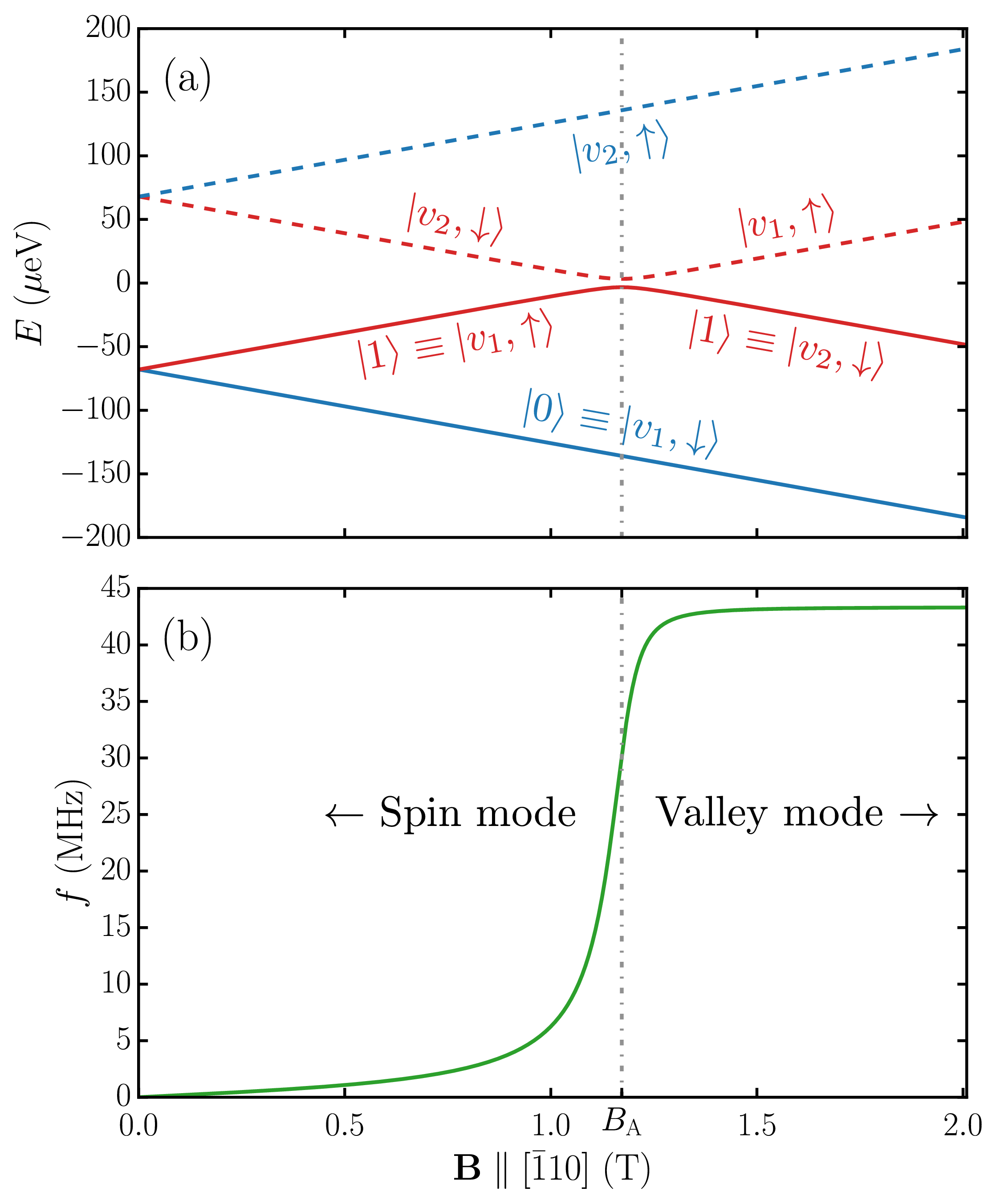
The energy of the spin-valley states is plotted as a function of in Fig. 1a. The states and are mixed by SOC and anti-cross at magnetic field . The energy of the upper (dashed red) and lower (solid red) branch of the anti-crossing read:
| (1) |
where is the matrix element of the spin-orbit coupling Hamiltonian between valleys and . The eigenstates of the upper and lower branch are, respectively:
| (2a) | ||||
| (2b) | ||||
with:
| (3a) | ||||
| (3b) | ||||
and:
| (4) |
Note that at , which highlights the strong mixing between spin and valley degrees of freedom near the anti-crossing. Although the states and do not anti-cross, we must for consistency account for a very small mixing by SOC (otherwise the Rabi frequency would not vanishCorna et al. (2018) when ) and introduce:
| (5a) | ||||
| (5b) | ||||
where , , and (, whatever ).
We are specifically interested in making a qubit based on states and . Qubit rotations are driven by a RF modulation on a front gate voltage . The Rabi frequency for the resonant transition between states and is then:
| (6) |
where is the amplitude of the RF signal ( meV hereafter), is the derivative of the total potential in the device with respect to , and is the gate coupling matrix element between valleys and .
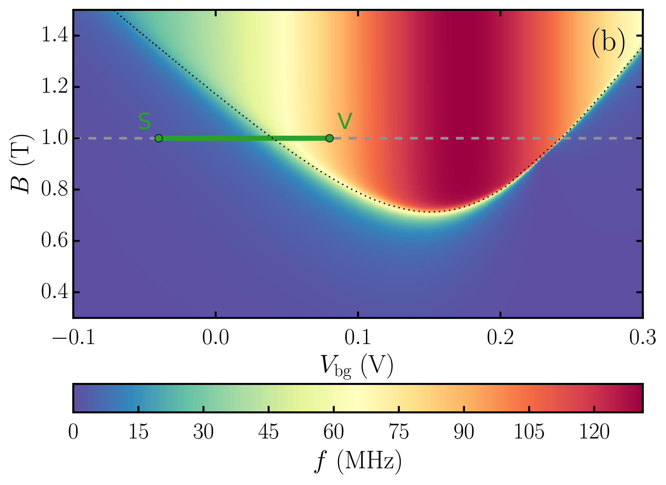
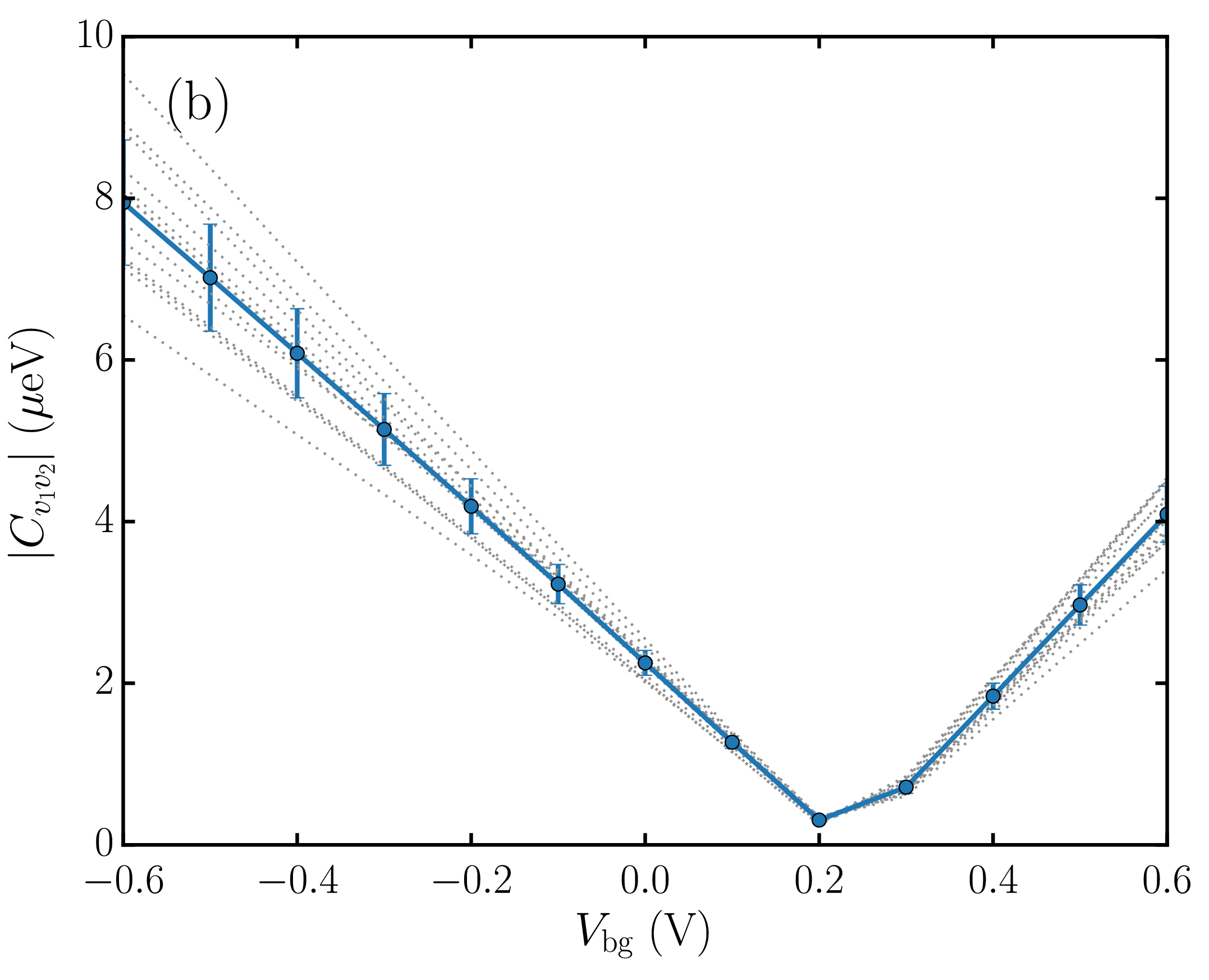
is plotted as a function of magnetic field in Fig. 1b, for values of , and extracted from tight-binding simulations on the device of Fig. 2 (see later discussion). For , , so that the device is an almost “pure spin” qubit,Loss and DiVincenzo (1998) which is hardly addressable electrically. When increasing , admixes a growing fraction of , which is coupled to the ground-state by the RF electric field, allowing for Rabi oscillations (mixed spin/valley qubit). For , , so that the device eventually becomes an almost “pure valley” qubit.Schoenfield et al. (2017) The maximum Rabi frequency in this regime, , is therefore limited by the gate coupling matrix element . The width of the transition near is controlled by the SOC matrix element , which sets the anti-crossing gap at . The Rabi frequency may also depend on the orientation of the magnetic field (as the spin is quantized along in the definition of ).
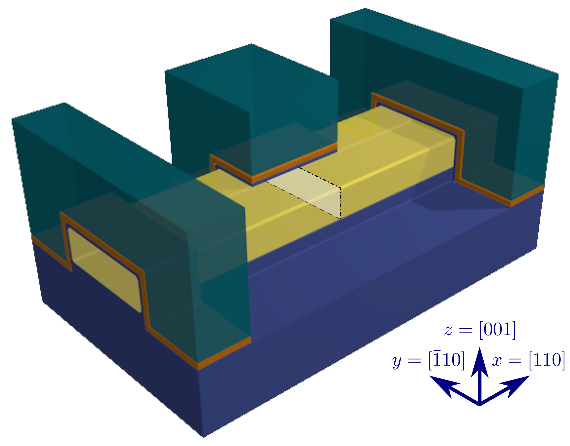
The signatures of this spin resonance mechanism have been observed in a silicon nanowire device.Corna et al. (2018) A model for this device is shown in Fig. 2. The quantum dot is defined by a central gate on a silicon channel with rectangular cross section etched on a SOI substrate. The gate overlaps only half of the channel. The electrons are hence confined in “corner dots” at the edge of the channel covered by the gate.Voisin et al. (2014) As discussed in Ref. Corna et al., 2018, the formation of such low-symmetry dots is a key ingredient of the present spin resonance mechanism. Indeed, is zero when the magnetic field is perpendicular to a mirror plane; as an illustration, the Rabi frequency measured in Ref. Corna et al., 2018 is minimal when is along the nanowire, and maximal when is perpendicular to the nanowire, because is a mirror plane in Fig. 2. Consequently, SOC is inefficient in highly symmetric dots with more than one symmetry plane.
As discussed above, the Rabi frequency is maximal beyond the anti-crossing between and and can reach a few tens to a hundred of MHz depending on the device design and disorder.Corna et al. (2018) This is much larger than the Rabi frequencies achieved with extrinsic elements such as micro-magnets. However, a QD operating in this regime would not make a good qubit. Indeed, the vicinity of the anti-crossing and the valley mode beyond are known to be “hot spots” for relaxationYang et al. (2013); Huang and Hu (2014) (shorter ) and decoherence (shorter due to enhanced sensitivity to charge and gate noise). Also, the strong mixing between and states near the anti-crossing may complicate the management of exchange interactions between neighboring qubits.
It would, therefore, be highly desirable to bring the qubit in the valley regime (beyond the anti-crossing) in order to manipulate its state electrically, then back to the spin regime (before the anti-crossing) once rotations are completed. The transitions between the two regimes must be performed adiabatically in order to achieve well defined operations.
The most obvious way to tune the spin/valley mixing is to vary the amplitude of the external magnetic field (see Fig. 1). However, fast variations of are unrealistic, and would affect all qubits at once. An other way is to control the valley splitting with the gate(s). It has already been demonstrated that the valley splitting at a Si/SiO2 interface depends on the electric field at that interface,Goswami et al. (2007); Yang et al. (2013) and can span orders of magnitudes. Nonetheless, it is generally difficult to control both the confinement potential and the vertical electric field with a set of front gates, which limits the range of achievable valley splittings. In SOI devices, the presence of both a front and a back gate allows, in principle, to decouple the confinement potential from the vertical electric field, and to implement electrical manipulation schemes based on the control of the valley splitting more easily.
In order to illustrate this, we have performed tight-binding (TB) calculations using the model of Ref. Niquet et al., 2009. This model accounts for valley and spin-orbit coupling at the atomistic level. The potential in the device is first computed with a finite volumes Poisson solver, then the eigenstates of the TB Hamiltonian in this potential are calculated with a Jacobi-Davidson eigensolver. The Rabi frequencies are finally obtained from Eq. (6), and spin manipulations are simulated with a time-dependent Schrödinger-Poisson solver in the basis of the 128 lowest-lying conduction band states of the QD. The atomistic segment of the device is 80 nm long and contains around atoms. The dangling bonds at the surface of the channel are saturated with pseudo-hydrogen atoms.
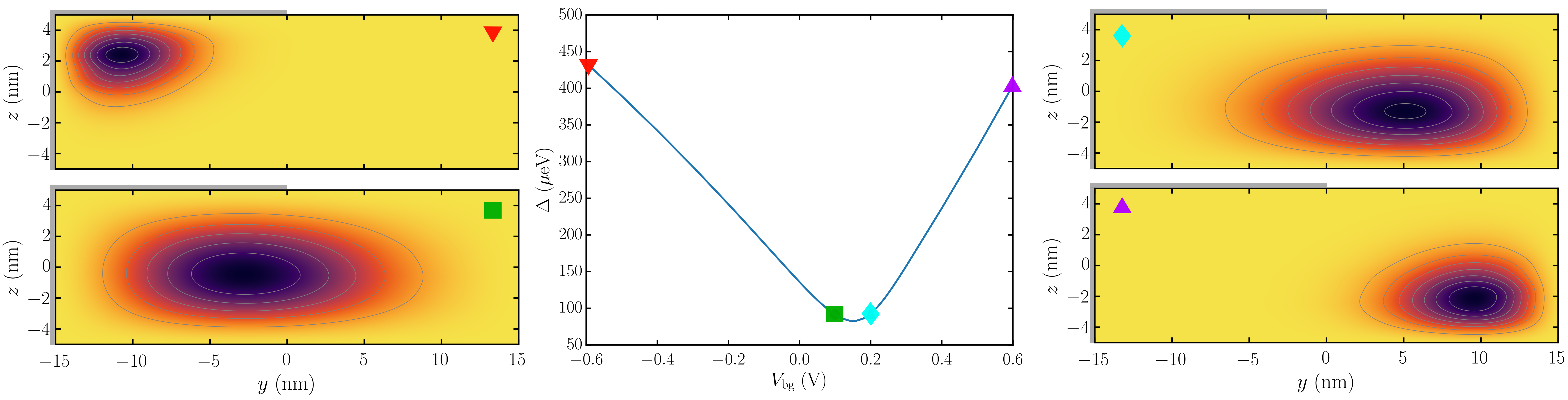
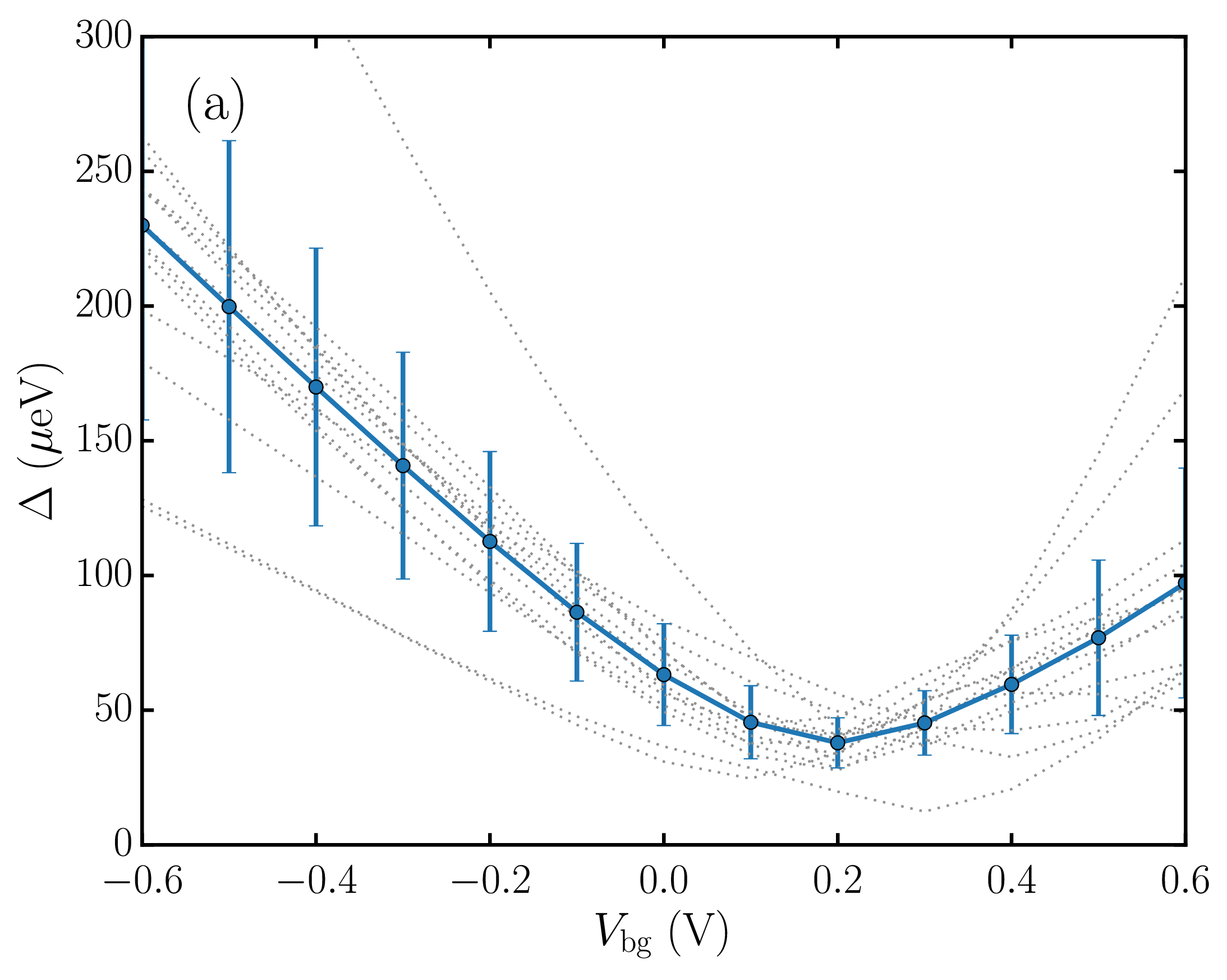
We first consider an “ideal” device without surface roughness disorder. The valley splitting is plotted as a function of the back gate voltage at fixed front gate voltage V in Fig. 3. decreases linearly with increasing , then reaches a minimum in the 80 eV range, and finally increases linearly again. During the back gate voltage sweep, the wave function of the electron moves from the top (negative ) to the bottom (positive ) interface, but remains confined under the top gate. The valley splitting increases when the wavefunction is further squeezed at one of the two interfaces by the vertical electric field, and is minimal when the electron is centered between the two interfaces. Although our model for the surface is simplified, the existing experimental data suggest that small valley splittings can indeed be achieved in SOI devices.Corna et al. (2018) Also, test calculations made with the model of Ref. Kim et al., 2011 for the Si/SiO2 interfaces show exactly the same trends.
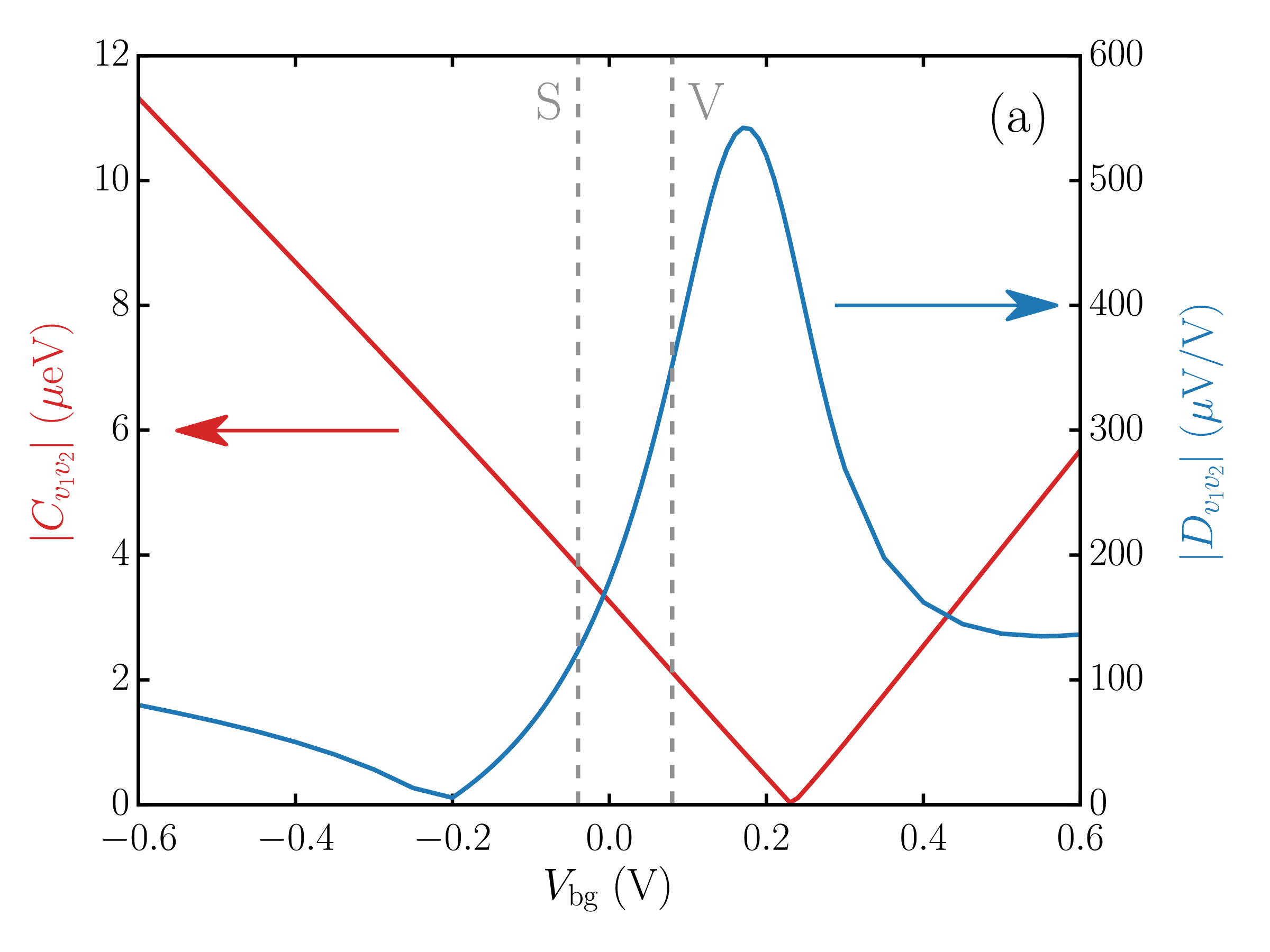
and are plotted as a function of in Fig. 4a. They are little dependent on the magnitude of the magnetic field . just above because the electron wave function, almost perfectly centered between the two gates, shows two additional horizontal and vertical quasi-symmetry planes.Corna et al. (2018) is, on the other hand, maximum near because deconfinement in the plane enhances coupling to the component of the RF electric field.
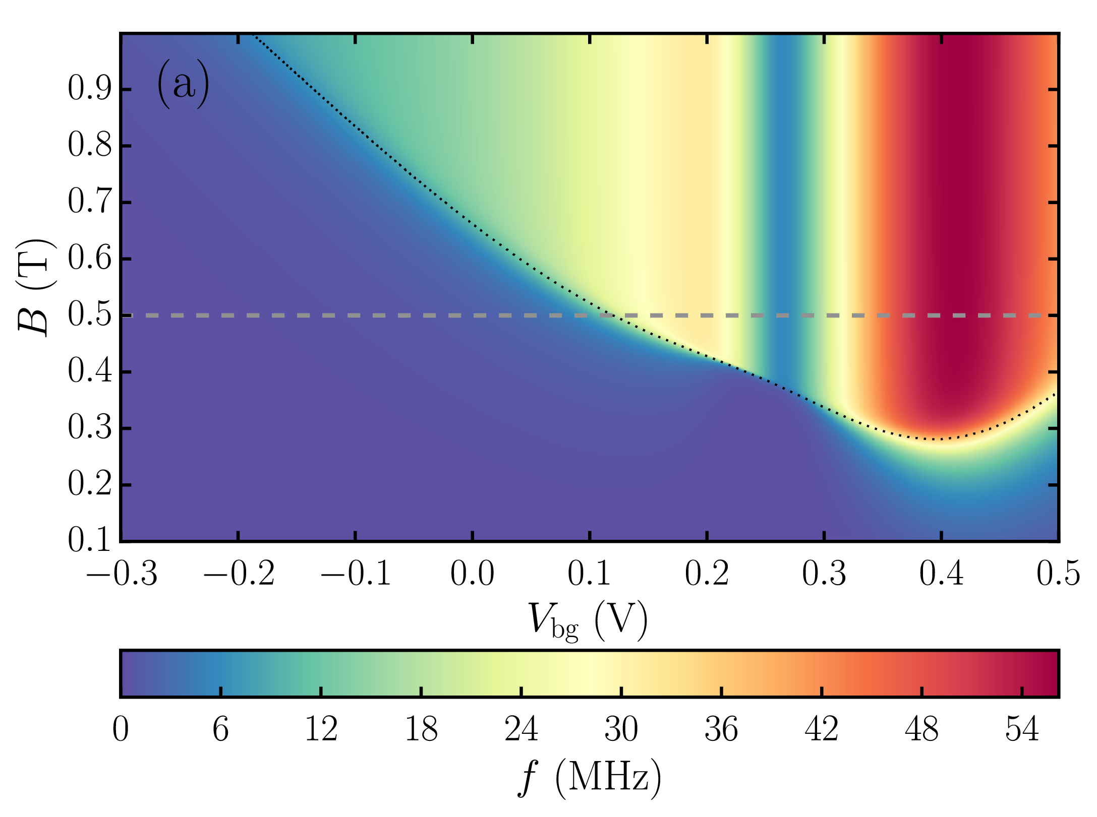
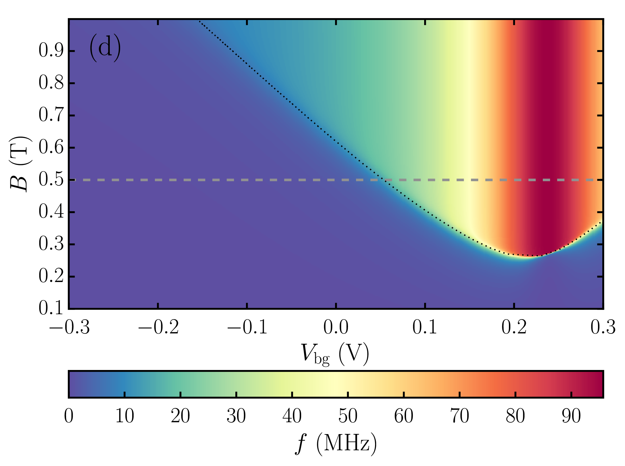
The calculated Rabi frequency is plotted as a function of and in Fig. 4b. The Rabi frequency is sizable within a hyperbolic-like shape whose edges are defined by the anti-crossing condition . Indeed, for a given magnetic field , there are typically zero or two back gate voltages that meet this condition (see Fig. 3 and dotted line in Fig. 4b). The qubit goes in the valley regime inside the hyperbolic-like shape, and in the spin regime outside. The calculated Rabi frequency reaches values as large as 120 MHz near where is maximum.
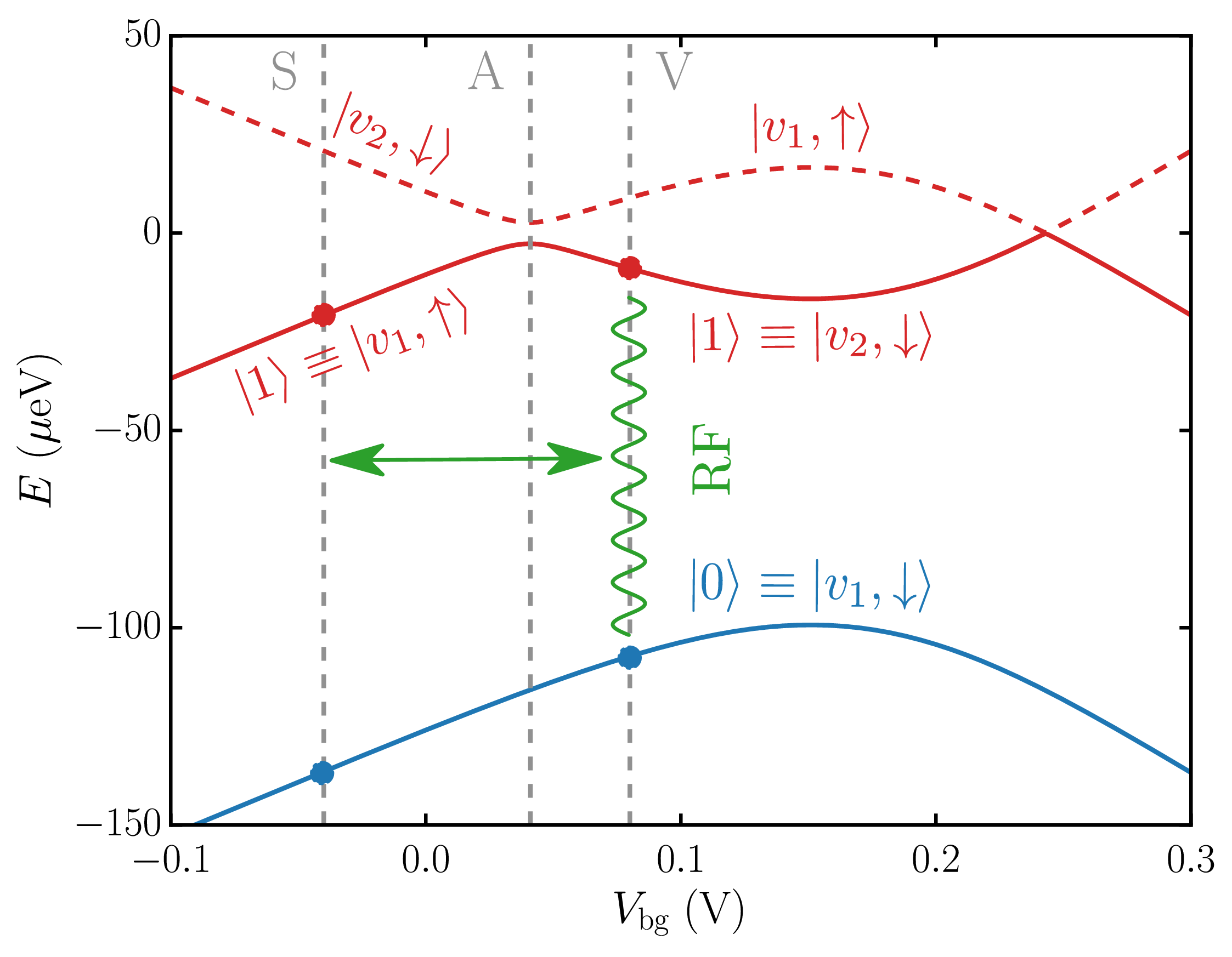
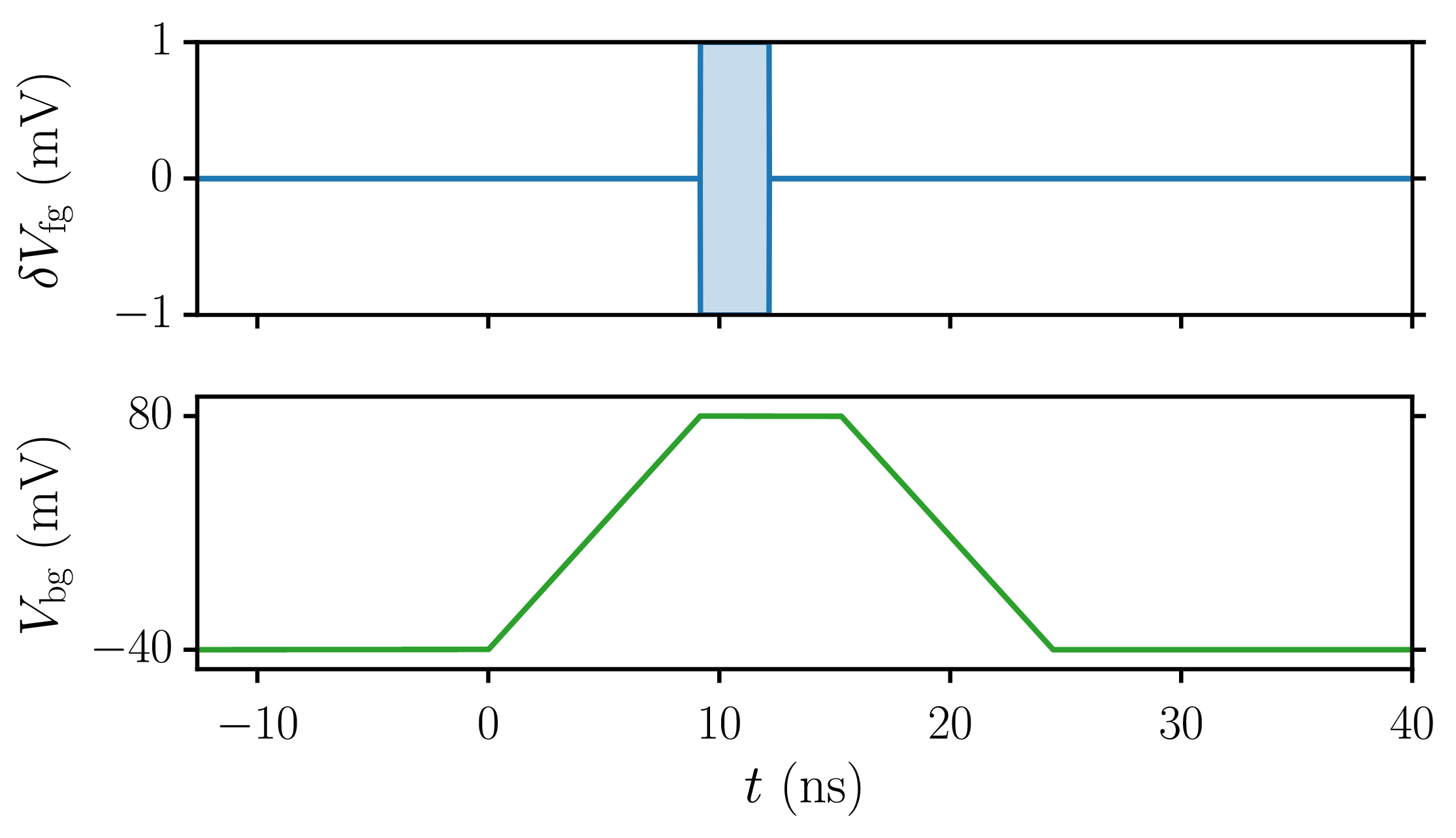
We can now design an electrical manipulation scheme taking advantage of Fig. 4. We set T along and bias the qubit along the line from point point S ( V) to point V ( V). At point V, the qubit is indeed in the valley regime and can be efficiently manipulated by the front gate (Rabi frequency MHz). On the opposite, the qubit is in the spin regime at reference point S; the Rabi frequency is almost zero but the qubit is presumably much more robust to inelastic relaxation and decoherence than at point V. The energy levels along [SV] are plotted in the top panel of Fig. 5.
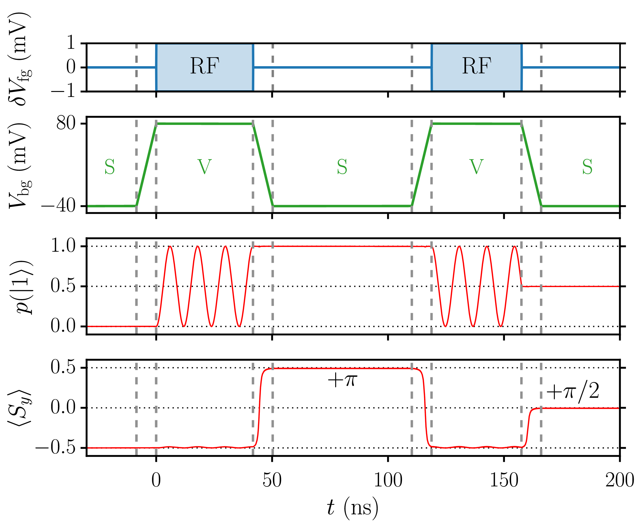
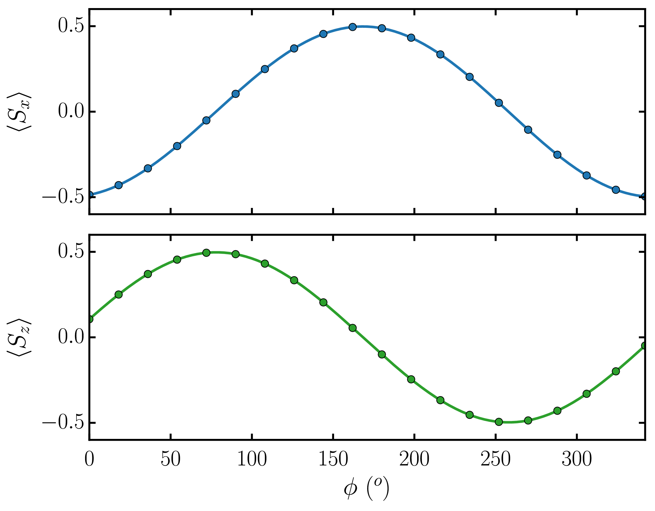
The manipulation protocol is illustrated in the bottom panels of Fig. 5, which represent the probability to be in the state and the expectation value of the spin along as a function of time during a and a rotation. The qubit is prepared in the state at point S, then switched to point V for manipulation. A RF pulse is applied on the front gate in order to drive a rotation, and the qubit is finally moved back to point S. The sequence is repeated for a subsequent rotation. Note that the system undergoes Rabi oscillations between states and at point V; therefore, remains almost constant at point V on Fig. 5. However, at point S, , so that the spin rotations are completed by SOC on the way back from V to S.not It is important to sweep between S and V adiabatically enough so that the system remains on the lower branch of the anti-crossing and does not couple to the upper branch (which would result into a mixed spin/valley rotation back at point S). The slew rate on is primarily limited by the gap between and at the anti-crossing point A,Zener (1932) . Here, eV is sufficiently large to achieve adiabatic switching within ns. The possibility to drive arbitrary rotations is further demonstrated in the Supporting Information.
In order to assess spin coherence at points S and V, we have computed the relaxation time due to phonons and Johnson-Nyquist (JN) noise. We follow Refs. Tahan and Joynt, 2014; Huang and Hu, 2014 and assume a series resistance on the front gate. We find that the operation of the qubit is limited by JN relaxation, with ms at point S, and s at point V. As expected, the lifetimes are much longer in the spin than in the valley qubit regime, which is the rationale for this manipulation protocol. In the valley regime, might be strongly limited by the noise;Paladino et al. (2014) we point out, though, that there is a sweet spot near , where the sensitivity of the valley splitting to gate and charge noise is minimal. More details about the models for and can be found in the Supporting Information.
We have also investigated the effects of surface roughness disorder on the Rabi frequencies (see Supporting Information). Surface roughness disorder reduces the valley splitting and is responsible for significant device-to-device variability. However, the valley-splitting shows a minimum in the eV range near the same in most devices, making the above manipulation protocol still possible with a proper calibration of each qubit. The Rabi frequencies are smaller because surface roughness reduces ,Culcer et al. (2010) yet they remain significant (typically MHz).
To conclude, we have demonstrated that the mixing between the spin and valley degrees of freedom in a silicon qubit can be controlled by a suitable engineering of the electric field. Thanks to the weak, but sizable spin-orbit coupling in the conduction band, the qubit can be continuously switched from a “spin” to a mixed “spin-valley” and eventually a “valley” mode by the action on the gates. In the spin-valley and valley modes, Rabi oscillations can be driven by radio-frequency signals on the gates, allowing for all-electrical manipulation schemes. In the pure spin mode, the qubit is not electrically addressable but is much more robust to inelastic relaxation and decoherence. A spin qubit may hence be switched to the valley mode for electrical manipulation then back to the spin mode in order to benefit from the long spin coherence times afforded by silicon. These findings open new perspectives for the development of efficient and scalable spin qubits on silicon. They also confirm that the effects of spin-orbit coupling in the conduction band of silicon are far from negligible, and can even be tailored for practical applications.
We thank Louis Hutin, Benoît Bertrand and Silvano de Franceschi for fruitful discussions. This work was supported by the European Union’s Horizon 2020 research and innovation program under grant agreement No 688539 MOSQUITO. Part of the calculations were run on the TGCC/Curie and CINECA/Marconi machines using allocations from GENCI and PRACE.
References
- Zwanenburg et al. (2013) F. A. Zwanenburg, A. S. Dzurak, A. Morello, M. Y. Simmons, L. C. L. Hollenberg, G. Klimeck, S. Rogge, S. N. Coppersmith, and M. A. Eriksson, Review of Modern Physics 85, 961 (2013).
- Tyryshkin et al. (2012) A. M. Tyryshkin, S. Tojo, J. J. L. Morton, H. Riemann, N. V. Abrosimov, P. Becker, P. H. J., T. Schenkel, M. L. W. Thewalt, K. M. Itoh, and S. A. Lyon, Nature Materials 11, 143 (2012).
- Veldhorst et al. (2015a) M. Veldhorst, C. H. Yang, J. C. C. Hwang, W. Huang, J. P. Dehollain, J. T. Muhonen, S. Simmons, A. Laucht, F. E. Hudson, K. M. Itoh, A. Morello, and A. S. Dzurak, Nature 526, 410 (2015a).
- Takeda et al. (2016) K. Takeda, J. Kamioka, T. Otsuka, J. Yoneda, T. Nakajima, M. R. Delbecq, S. Amaha, G. Allison, T. Kodera, S. Oda, and S. Tarucha, Science Advances 2, e1600694 (2016).
- Veldhorst et al. (2014) M. Veldhorst, J. C. C. Hwang, C. H. Yang, A. W. Leenstra, B. de Ronde, J. P. Dehollain, J. T. Muhonen, F. E. Hudson, K. M. Itoh, A. Morello, and A. S. Dzurak, Nature Nanotechnology 9, 981 (2014).
- Veldhorst et al. (2015b) M. Veldhorst, R. Ruskov, C. H. Yang, J. C. C. Hwang, F. E. Hudson, M. E. Flatté, C. Tahan, K. M. Itoh, A. Morello, and A. S. Dzurak, Physical Review B 92, 201401(R) (2015b).
- Laucht et al. (2015) A. Laucht, J. T. Muhonen, F. A. Mohiyaddin, R. Kalra, J. P. Dehollain, S. Freer, F. E. Hudson, M. Veldhorst, R. Rahman, G. Klimeck, K. M. Itoh, D. N. Jamieson, J. C. Mccallum, A. S. Dzurak, and A. Morello, Science Advances 1, e1500022 (2015).
- Pioro-Ladrière et al. (2008) M. Pioro-Ladrière, T. Obata, Y. Tokura, Y.-S. Shin, T. Kubo, K. Yoshida, T. Taniyama, and S. Tarucha, Nature Physics 4, 776 (2008).
- Kawakami et al. (2014) E. Kawakami, P. Scarlino, D. R. Ward, F. R. Braakman, D. E. Savage, M. G. Lagally, M. Friesen, S. N. Coppersmith, M. A. Eriksson, and L. M. K. Vandersypen, Nature Nanotechnology 9, 666 (2014).
- Nowack et al. (2007) K. C. Nowack, F. H. L. Koppens, Y. V. Nazarov, and L. M. K. Vandersypen, Science 318, 1430 (2007).
- Nadj-Perge et al. (2010) S. Nadj-Perge, S. M. Frolov, E. P. A. M. Bakkers, and L. P. Kouwenhoven, Nature 468, 1084 (2010).
- Pribiag et al. (2013) V. S. Pribiag, S. Nadj-Perge, S. M. Frolov, J. W. G. van den Berg, I. van Weperen, S. R. Plissard, E. P. A. M. Bakkers, and L. P. Kouwenhoven, Nature Nanotechnology 8, 170 (2013).
- Maurand et al. (2016) R. Maurand, X. Jehl, D. Kotekar-Patil, A. Corna, H. Bohuslavskyi, R. Laviéville, L. Hutin, S. Barraud, M. Vinet, M. Sanquer, and S. de Franceschi, Nature Communications 7, 13575 (2016).
- Huang et al. (2017) W. Huang, M. Veldhorst, N. M. Zimmerman, A. S. Dzurak, and D. Culcer, Physical Review B 95, 075403 (2017).
- Corna et al. (2018) A. Corna, L. Bourdet, R. Maurand, A. Crippa, D. Kotekar-Patil, H. Bohuslavskyi, R. Laviéville, L. Hutin, S. Barraud, X. Jehl, M. Vinet, S. De Franceschi, Y.-M. Niquet, and M. Sanquer, npj Quantum Information 4, 6 (2018).
- Nestoklon et al. (2006) M. O. Nestoklon, L. E. Golub, and E. L. Ivchenko, Physical Review B 73, 235334 (2006).
- Sham and Nakayama (1979) L. J. Sham and M. Nakayama, Physical Review B 20, 734 (1979).
- Saraiva et al. (2009) A. L. Saraiva, M. J. Calderon, X. Hu, S. Das Sarma, and B. Koiller, Physical Review B 80, 081305(R) (2009).
- Friesen and Coppersmith (2010) M. Friesen and S. N. Coppersmith, Physical Review B 81, 115324 (2010).
- Culcer et al. (2010) D. Culcer, X. Hu, and S. Das Sarma, Physical Review B 82, 205315 (2010).
- Goswami et al. (2007) S. Goswami, K. A. Slinker, M. Friesen, L. M. McGuire, J. L. Truitt, C. Tahan, L. J. Klein, J. O. Chu, P. M. Mooney, D. W. van der Weide, R. Joynt, S. N. Coppersmith, and M. A. Eriksson, Nature Physics 3, 41 (2007).
- Yang et al. (2013) C. H. Yang, A. Rossi, R. Ruskov, N. S. Lai, F. A. Mohiyaddin, S. Lee, C. Tahan, G. Klimeck, A. Morello, and A. S. Dzurak, Nature Communications 4, 2069 (2013).
- Mi et al. (2017) X. Mi, C. G. Péterfalvi, G. Burkard, and J. R. Petta, Physical Review Letters 119, 176803 (2017).
- Hao et al. (2014) X. Hao, R. Ruskov, M. Xiao, C. Tahan, and H. Jiang, Nature Communications 5, 3860 (2014).
- Scarlino et al. (2017) P. Scarlino, E. Kawakami, T. Jullien, D. R. Ward, D. E. Savage, M. G. Lagally, M. Friesen, S. N. Coppersmith, M. A. Eriksson, and L. M. K. Vandersypen, Physical Review B 95, 165429 (2017).
- Huang and Hu (2014) P. Huang and X. Hu, Physical Review B 90, 235315 (2014).
- Schoenfield et al. (2017) J. S. Schoenfield, B. M. Freeman, and H. Jiang, Nature Communications 8, 64 (2017).
- Loss and DiVincenzo (1998) D. Loss and D. P. DiVincenzo, Physical Review A 57, 120–126 (1998).
- Kloeffel et al. (2013) C. Kloeffel, M. Trif, P. Stano, and D. Loss, Physical Review B 88, 241405 (2013).
- Voisin et al. (2014) B. Voisin, V.-H. Nguyen, J. Renard, X. Jehl, S. Barraud, F. Triozon, M. Vinet, I. Duchemin, Y. M. Niquet, S. de Franceschi, and M. Sanquer, Nano Letters 14, 2094 (2014).
- Niquet et al. (2009) Y. M. Niquet, D. Rideau, C. Tavernier, H. Jaouen, and X. Blase, Physical Review B 79, 245201 (2009).
- Kim et al. (2011) S. Kim, M. Luisier, A. Paul, T. B. Boykin, and G. Klimeck, IEEE Transactions on Electron Devices 58, 1371 (2011).
- (33) In essence, we dissociate here the action of the RF field and the action of SO coupling with respect to a conventional EDSR set-up, where SO coupling would act on the spin during the RF excitation.
- Zener (1932) C. Zener, Proceedings of the Royal Society of London A: Mathematical, Physical and Engineering Sciences 137, 6962 (1932).
- Tahan and Joynt (2014) C. Tahan and R. Joynt, Physical Review B 89, 075302 (2014).
- Paladino et al. (2014) E. Paladino, Y. M. Galperin, G. Falci, and B. L. Altshuler, Review of Modern Physics 86, 361 (2014).
Supporting Information for “All-electrical manipulation of silicon spin qubits with tunable spin-valley mixing”
In this Supporting Information, we provide a line cut on on Fig. 4 of the main text (section I), then discuss the nature of the rotations performed with the present manipulation protocol (section II), and finally the effects of surface roughness (section III) and the calculation of (section IV).
I Line cut on Fig. 4 of the main text.
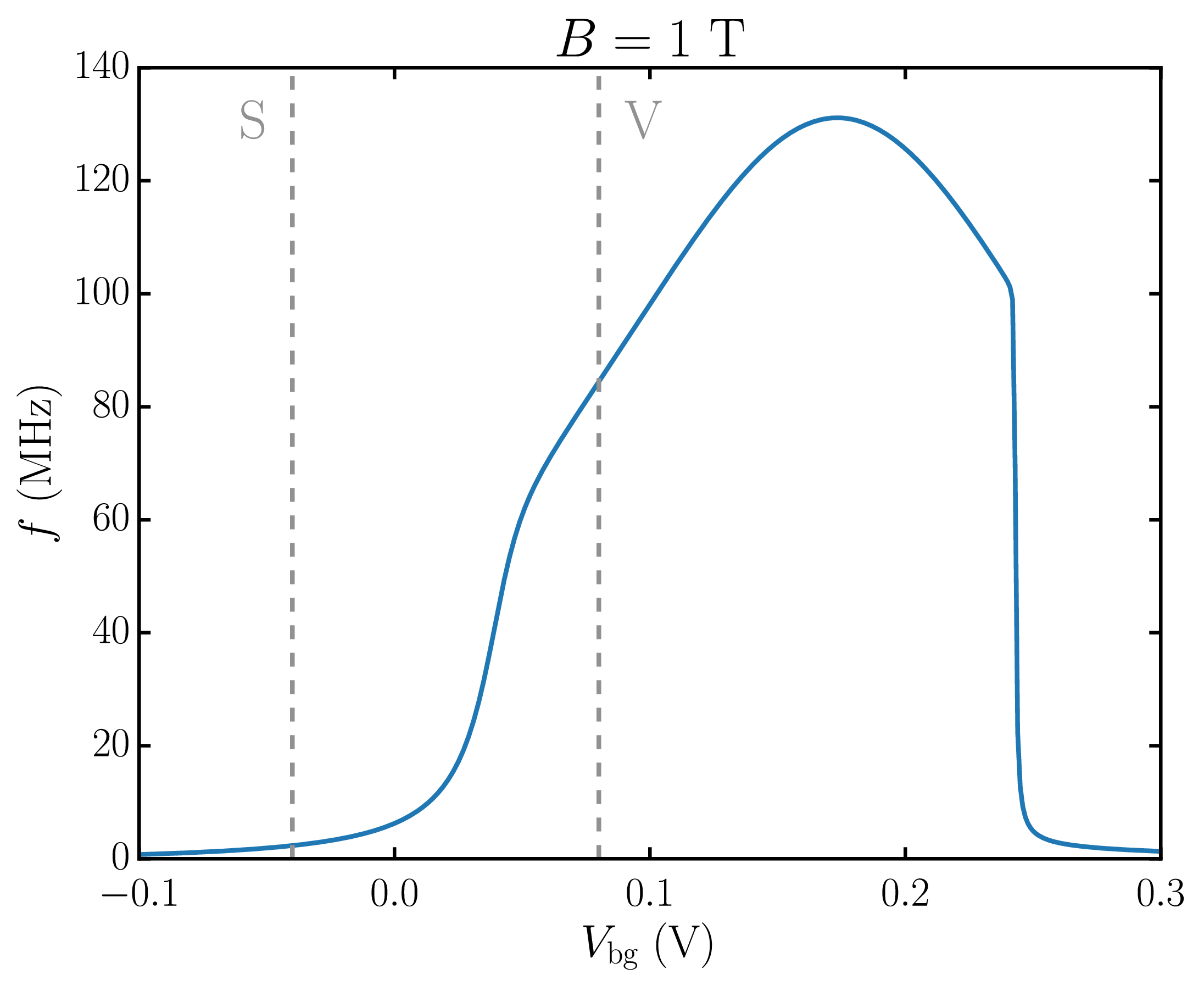
The Rabi frequency is plotted in Fig. S1 along the horizontal dashed line of Fig. 4b, main text. The width of the transitions from the spin to the valley qubit regimes is controlled by the SOC matrix element , while the Rabi frequency in the valley qubit regime is essentially set by the gate coupling matrix element (Fig. 4a).
II Nature of the rotations.
During the manipulation sequence, the phase of the qubit drifts on the way from S to V then from V to S, as well as during the rotation at V, since the precession frequencies are slightly different at the S and V points. Let us, therefore, introduce the time-dependent states and , where is the precession frequency at point S. The projections of the qubit state on and define its representation in the rotating Bloch sphere at point S.
The transformation matrix for the manipulation sequence reads in the basis set:
| (S1) |
where is the matrix of a rotation of angle around the polar axis of the Bloch sphere:
| (S2) |
and is the matrix of a rotation of angle around :
| (S3) |
, and are the phase shifts accumulated on the way from S to V, at the V point, and back from V to S. and depend on the back gate voltage ramps, while , where and are the precession frequency and the total time spent at point V, respectively. is controlled by the duration of the RF pulse at V. The axis of rotation, characterized by , can in principle be controlled by the phase of the RF signal, as demonstrated below.
The above sequence of rotations can be factorized as:
| (S4) |
Namely, the net operation appears as a rotation around an axis of the equatorial plane of the Bloch sphere (as expected), followed by a rotation around that accounts for the total phase accumulated out of the S point. This phase must be accounted for when chaining rotations. It can be compensated by choosing such that irrespective of the rotation (typically, must be greater than so that rotations can be accommodated within the manipulation window at V).
As an illustration, figure S2 shows the expectation value of and in the rotating Bloch sphere after a rotation from the state, as a function of the phase of the RF signal on the front gate [namely, ]. The magnetic field is parallel to . This figure confirms that rotations can be driven around arbitrary axes of the equatorial plane of the rotating Bloch sphere by controlling the phase of the RF signal, as done in conventional ESR/EDSR experiments.
In this figure, the time spent at the V point has been adjusted so that two successive rotations around the same axis result in a net rotation (). Still, the phase of the second rotation must account for the mismatch in precession frequencies at S and V. For example, if the first rotation at time is driven by a RF signal , the second rotation at time must be driven by a RF signal .
III Effects of surface roughness.
In order to assess the robustness and variability of the results, we have introduced surface roughness (SR) disorder in the simulations. The SR profiles are generated from a Gaussian spectral density with rms nm and correlation length nm.Goodnick et al. (1985) lies in the upper range of the values compatible with the carrier mobilities measured in similar devices at room temperature.Bourdet et al. (2016) The SR profiles are, therefore, pretty aggressive. Surface roughness might be mitigated with suitable annealing techniques.Dornel et al. (2007)
The valley-splitting is plotted as a function of the back gate voltage in Fig. S3a for different realizations of the disorder. Although the slope of shows significant variability on both front and back interfaces, most curves show a minimum in the eV range. is smaller with SR ( eV without), because roughness averages out part of the valley interactions.Culcer et al. (2010) This brings the manipulation frequency in the valley qubit regime down to the GHz range, which is easily accessible with standard RF circuitry.
The matrix elements and are plotted in Fig. S3b and S3c for different realizations of the disorder. They are, likewise, both decreased by the roughness. shows little variability, while the shape and magnitude of can be strongly dependent on the particular realization of the SR, especially near due to the complex interference pattern between the top and down interfaces. This may lower the achievable Rabi frequencies, but does not, in general, preclude the proposed manipulation protocol at the price of a calibration of each qubit. This is illustrated in Fig. S4, which shows maps of the Rabi frequency as a function of the magnetic field and for four different realizations of the disorder. Although some maps might show a more complex behavior than Fig. 4 of the main text, the qubit remains electrically addressable over a wide range of back gate voltages within the valley regime. The calculated Rabi frequencies typically reach a few tens of MHz, which is still very significant.
IV Calculation of and .
We compute the relaxation rate due to the electron-phonon interactions in the electric dipole approximation.Tahan and Joynt (2014); Huang and Hu (2014) The contribution from longitudinal phonons reads:
| (S5) |
while the contribution from transverse phonons reads:
| (S6) |
where is the qubit precession frequency, , and are the dipole matrix elements in the device axis set, m/s and m/s are the longitudinal and transverse sound velocities, eV and eV are the conduction band deformation potentials, kg/m3 is the mass density of silicon, and mK is the temperature.
We follow Refs. Huang and Hu, 2014, Clerk et al., 2010 and Paladino et al., 2014 for Johnson-Nyquist noise. We assume a series resistance on the front gate so that:
| (S7) |
where , , and .
The relevant data at the S and V points are given in Table 1 for the device of the main text. As expected, and are much longer in the spin than in the valley regime due to the reduced sensitivity of spin qubits to electric fields. The operation of the qubit is limited by Johnson Nyquist noise, but the calculated remains orders of magnitude larger than the total manipulation time (a few tens of ns on Fig. 5, main text and on Fig. S2). The phonon-limited ’s are also much longer than measured in Ref. Yang et al., 2013 because the valley splittings and dipole matrix elements are smaller (in particular, and scale as in the valley regime). Practically, the coherence might be limited by various sources of noisePaladino et al. (2014) (charge and gate noise, …), which still need to be carefully characterized.
| S point | V point | |
|---|---|---|
| (eV) | 115.3 | 98.3 |
| (Å) | 0.000 | 0.001 |
| (Å) | 0.005 | 0.050 |
| (Å) | 0.011 | 0.287 |
| (V/V) | 9.5 | 348.9 |
| (V/V) | 2.4 | 607.8 |
| (s-1) | 1.02 | 3.08 |
| (s-1) | 0.15 | 32.8 |
| (s-1) | 15.4 | 1.77 |
| (s-1) | 3.64 | 2.35 |
References
- Goodnick et al. (1985) Goodnick, S. M.; Ferry, D. K.; Wilmsen, C. W.; Liliental, Z.; Fathy, D.; Krivanek, O. L. Physical Review B 1985, 32, 8171.
- Bourdet et al. (2016) Bourdet, L.; Li, J.; Pelloux-Prayer, J.; Triozon, F.; Cassé, M.; Barraud, S.; Martinie, S.; Rideau, D.; Niquet, Y.-M. Journal of Applied Physics 2016, 119, 084503.
- Dornel et al. (2007) Dornel, E.; Ernst, T.; Barbé, J. C.; Hartmann, J. M.; Delaye, V.; Aussenac, F.; Vizioz, C.; Borel, S.; Maffini-Alvaro, V.; Isheden, C.; Foucher, J. Applied Physics Letters 2007, 91, 233502.
- Culcer et al. (2010) Culcer, D.; Hu, X.; Das Sarma, S. Physical Review B 2010, 82, 205315.
- Tahan and Joynt (2014) Tahan, C.; Joynt, R. Physical Review B 2014, 89, 075302.
- Huang and Hu (2014) Huang, P.; Hu, X. Physical Review B 2014, 90, 235315.
- Clerk et al. (2010) Clerk, A. A.; Devoret, M. H.; Girvin, S. M.; Marquardt, F.; Schoelkopf, R. J. Review of Modern Physics 2010, 82, 1155.
- Paladino et al. (2014) Paladino, E.; Galperin, Y. M.; Falci, G.; Altshuler, B. L. Review of Modern Physics 2014, 86, 361.
- Yang et al. (2013) Yang, C. H.; Rossi, A.; Ruskov, R.; Lai, N. S.; Mohiyaddin, F. A.; Lee, S.; Tahan, C.; Klimeck, G.; Morello, A.; Dzurak, A. S. Nature Communications 2013, 4, 2069.