Implanting germanium into graphene
Abstract
Incorporating heteroatoms into the graphene lattice may be used to tailor its electronic, mechanical and chemical properties. Direct substitutions have thus far been limited to incidental Si impurities and P, N and B dopants introduced using low-energy ion implantation. We present here the heaviest impurity to date, namely 74Ge+ ions implanted into monolayer graphene. Although sample contamination remains an issue, atomic resolution scanning transmission electron microscopy imaging and quantitative image simulations show that Ge can either directly substitute single atoms, bonding to three carbon neighbors in a buckled out-of-plane configuration, or occupy an in-plane position in a divacancy. First principles molecular dynamics provides further atomistic insight into the implantation process, revealing a strong chemical effect that enables implantation below the graphene displacement threshold energy. Our results show that heavy atoms can be implanted into the graphene lattice, pointing a way towards advanced applications such as single-atom catalysis with graphene as the template.
Keywords: ion implantation, heteroatom doping, scanning transmission electron microscopy, electron spectroscopy, molecular dynamics
Graphene 1 is an atomically thin single layer of hexagonally bound carbon with remarkable thermal 2, mechanical 3, and electrical properties 4. This makes it an ideal material for applications ranging from composites to optoelectronics. However, for many purposes, the atomic structure of graphene is chemically too inert. One way to modify this is to incorporate heteroatoms as impurities into the structure, commonly introduced via a suitable chemical precursor during synthesis 5. However, due to a lack of control over their bonding and contamination by different chemical remnants, the quality of the produced structures is often limited 6, 7. An alternative is to use ion implantation.
Ion implantation is a mature technique to manipulate materials that offers great flexibility: a plethora of ion species, a wide range of implantation energies, and control over the dopant concentration through the ion fluence. It is widely used by the modern semiconductor industry to introduce controlled concentrations of p and n-type dopants at precise depths below crystal surfaces. Recently, single ions in semiconductors such as silicon, germanium and arsenic have attracted interest for the development of quantum computers 8. However, ion implantation is quite challenging in the case of two-dimensional (2D) materials such as graphene since only a narrow energy window will allow implantation—high enough to remove one or more target atoms yet low enough to stop the ion within the atomically thin structure 9. Moreover, since adatoms on 2D crystals tend to be mobile 10 and there are typically no available interstitial sites, the implanted ion needs to form covalent bonds with the under-coordinated atoms of the vacancy to reach a stable configuration. After early work on carbon nanotubes 11, 12, the direct substitutional doping of graphene 13, 14 and transition metal dichalcogenides 15 has been achieved using low-energy ion implantation, but large-scale controlled dopant incorporation into 2D materials remains an important challenge.
Germanium (Ge) is a structural and electronic analogue to silicon (Si), but significantly heavier (atomic number 32 as compared to 14) and larger (covalent atomic radius of 122 pm as compared to 111 pm for Si and 77 pm for C). This raises the question whether it could also be incorporated into graphene similar to the lighter boron and nitrogen 13, 16, the often observed silicon 17, 18, 19, and the recently implanted phosphorus 20, all of which are able to directly substitute for single C atoms. Due to its greater size, a significant increase of bond length resulting in threefold Ge buckling out of the plane is predicted 21. Its isovalence with Si anticipates 18 another possible bonding: a (nearly 22) planar fourfold substitution in a double vacancy. Based on density functional theory (DFT) calculations, doping graphene with germanium can open and control the band gap depending on concentration 23, 21. However, no experimental studies have yet been reported.
Results and discussion
We have successfully incorporated Ge into the graphene lattice using low-energy ion implantation. Although even our best implanted samples remain heavily contaminated 20, atomic resolution scanning transmission electron microscopy (STEM) shows that Ge can directly substitute for single atoms, bonding to three carbon neighbors in a buckled out-of-plane configuration as predicted by DFT. The chemical nature of the dopants is confirmed through quantitative image simulations and energy dispersive x-ray spectroscopy (EDX), whereas electron energy loss spectroscopy (EELS) is hardly sensitive to Ge due to spectral overlap with the much more intense graphene plasmon response 24. We describe the atomic-level details of the implantation process through ab initio molecular dynamics (MD) simulations, which reveal a strong chemical effect that reduces the required implantation energy for Ge as compared to purely kinematic arguments. This is experimentally verified by successful implantation below the carbon displacement threshold energy in graphene. Our results show for the first time that elements beyond the third period can be directly implanted into graphene, expanding the versatility of ion irradiation as a tool for engineering graphene.
Experimental
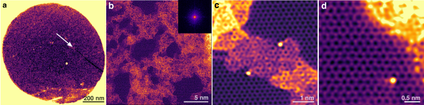
Contamination introduced during implantation degrades sample quality and makes characterization difficult. Like in previous P-implanted samples 20, most of the graphene surface is covered by a thick layer of contamination (a medium angle annular dark field, MAADF, image is presented in Fig. 1a), despite laser treatment both before and during the implantation (Methods). The degree of contamination was however not entirely consistent: in some samples we were not able to find any clean lattice despite extensive searching, whereas in others this was rare, but included regions with implanted impurity atoms. Due to this variation, which was greater than in earlier P-implanted graphene 20, we cannot exclude the possibility that our laser alignment varied between the different experiments.
Most of our data is from the cleanest sample that was irradiated at 20 eV. We did also find one incorporated impurity atom in a sample irradiated at 15 eV, but found no clean lattice in the sample irradiated at 25 eV. This lack of statistics from different ion energies prevents us from deducing the ideal implantation energy from the experimental data—in total, we found only seven Ge impurities directly in the lattice (roughly 1500 nm2 of clean lattice was analyzed; with our ion fluence of 1 ion/nm2, this yields an implantation efficiency of just 0.5%). An example of a relatively clean sample area is presented in Fig. 1b, illustrating how most clean areas do not contain any Ge atoms (or other defects). Examples of heavy impurities found in the contamination as well as incorporated into the lattice are presented in Figs. 1c,d.
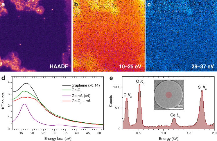
EELS is usually the best tool for establishing chemical identities and bonding at the atomic level 13, 16, 20. However, Ge impurities in graphene present a particular challenge: the weak Ge L-edge is located at 1150 eV, beyond the range of our spectrometer, whereas the M4,5-edge, located at 32 eV, falls under the much more intense graphene plasmon (which is further influenced by nearby contamination 26, 27). As a consequence, in the EEL spectrum maps of Figs. 2b,c, it is not possible to distinguish the signal of the Ge atoms from the background of the plasmon tail, even though the impurities are clearly visible in the simultaneously acquired high angle annular dark field (HAADF) image (Fig. 2a). Nonetheless, as shown in Fig. 2d, a high signal-to-noise spot spectrum recorded over a single Ge substitution shows an apparent splitting of the plasmon peak as well as additional intensity compared to pristine graphene at higher energy losses. Although subtracting a scaled reference spectrum of thin-film bulk Ge (Gatan EELS Atlas 28) with an intense plasmon component centered at 17 eV in addition to the M4,5-edge starting at 29 eV (Ref. 29) can partially account for both features, further studies with monochromated EELS 30 seem warranted. However, as shown in Fig. 2e, it is much easier to detect the spectroscopic signature of Ge using EDX, which should in a suitable instrument be feasible down to the single-atom level 31.
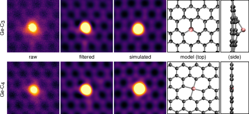
Due to the atomic number-dependent scattering contrast in annular dark field images 25, we can turn to quantitative image simulations to verify the identity of the observed impurities 32. The atomic resolution STEM images shown in Fig. 3 give two examples of an individual heavy impurity within the graphene lattice. To reduce the influence of the electron beam probe tails, these MAADF images have been processed using a double Gaussian filter 25. Scattering at the impurity is extremely intense even to the MAADF detector, making it difficult to distinguish the local structure. However, simulated images of threefold (Ge-C3) and fourfold (Ge-C4) germanium substitutions (Fig. 3) agree well with the filtered images. From HAADF images (that avoid nonlinear scattering effects present in MAADF images), we measure the ratio of the intensity of the impurity atom to that of carbon atoms distant from it as 21.50.9 for Ge-C3 and 21.71.0 for Ge-C4, with simulated ratios respectively of 21.8 and 22.5. This corresponds to a Ge/C contrast proportional to Z1.86, and the agreement confirms the chemical identity of the impurities. Our DFT simulation reproduces the significant structural rearrangement expected around the Ge-C3 site 21, with the Ge atom buckling 1.90 Å out of the graphene plane as shown in the top and side views of the relaxed model structure (Fig. 3).
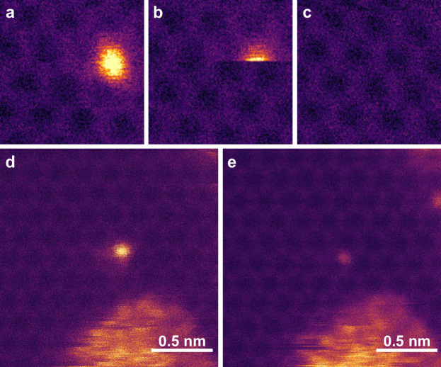
Finally, inspired by recent electron-beam manipulation of impurity atoms in graphene 19, 20, we attempted to move the Ge atoms by iteratively placing the electron beam on one C neighbor for 10 s between acquiring images. A total of 24 such irradiations were attempted on several different impurities, without success. DFT/MD simulations (described below) confirmed the reason: the beam-induced out-of-plane dynamics of the C atom, all the way up to its knock-on threshold of 15.75 eV, are unable to trigger the bond inversion mechanism 33 for Ge due to its greater mass and covalent radius. For Ge itself, the threshold energy is 11.75 eV, almost an order of magnitude more than what a 60-keV electron can transfer to such a heavy nucleus. However, we observed a curious effect: several Ge impurities got replaced by C (Fig. 4a-c) or, in one case, Si (Fig. 4d-e). Presumably the source of these atoms is the ubiquitous contamination, but the electron beam must somehow be involved in the mechanism (since otherwise we would not be able to find any Ge in the lattice).
Modeling
DFT-based molecular dynamics simulations were performed to analyse the energetics and atomic scale details of the implantation process. For successful incorporation of a heteroatom into graphene lattice by ion irradiation two conditions need to be satisfied: i) the energy transferred from the incident ion to carbon atom during collision is large enough to knock out carbon(s), and ii) the remaining kinetic energy of the ion after collision is low enough so that it stays in the structure. The energy transferred from the incident ion to a lattice atom is maximum for the case of a head-on collision, and therefore such impacts are most efficient in satisfying the above conditions. We observed a number of outcomes depending on the kinetic energy of the incident Ge ion. Ions with energies below 20 eV typically cannot induce breaking of the C-C bonds and thus remain on the graphene surface as adatoms. For ion energies between 20–22 eV, Ge substitutes carbon atom in the lattice; however, the displaced carbon is not sputtered but remains bound to the system. All our simulations show that such configurations relax spontaneously to a structure consisting of non-defective graphene with a Ge adatom (although this may not be the case in experiments at room temperature). For Ge energies of 23–25 eV, a Ge-C dimer is formed that flies away from the graphene layer, in which a monovacancy defect is formed. Finally, at 26 eV Ge is directly implanted into graphene structure while the C atom is sputtered. According to our calculations, direct implantation occurs for Ge kinetic energies ranging from 26 to 42 eV, while ions with higher energy penetrate through the graphene layer.
We find that in a head-on collision, an incident Ge ion transfers about 49% of its initial kinetic energy to an isolated carbon atom. The maximum kinetic energy of the impacted C atom in graphene is slightly less, 10.7 eV (41%) for an ion energy of 26 eV (Fig. 5). This is significantly lower than the threshold energy for displacement of carbon in graphene, calculated with our method as 22.3 eV. Evidently, interactions between the incident Ge ion and C atoms in graphene significantly lower the displacement threshold energy of carbon.
To obtain a more detailed picture of the process, we analyse the kinetic energies of the incident Ge ion (), sputtered C atom (), remaining C atoms in the graphene layer () and the total kinetic energy of the system () at each time step of the simulation for an initial ion energy of 26 eV (Fig. 5). At the beginning of the simulation, the total kinetic energy of the system equals that of the Ge ion. It slightly increases when the ion approaches graphene, with a maximum value of 27.8 eV, and starts to decrease quickly when the separation between the ion and graphene plane becomes less than 2.2 Å. The shortest Ge-C distance was found to be 1.53 Å. The energy transfer between the incident ion and the carbon atom occurs over tens of fs. When its kinetic energy reaches its maximum value of 10.7 eV, the C is already displaced from graphene plane (Fig. 5c) and, therefore, the maximum of can be lower than the actual amount of the transferred energy. Subsequently, the kinetic energy of the sputtered C atom drops quickly by about 6 eV and then gradually decreases to a constant value of 0.92 eV.
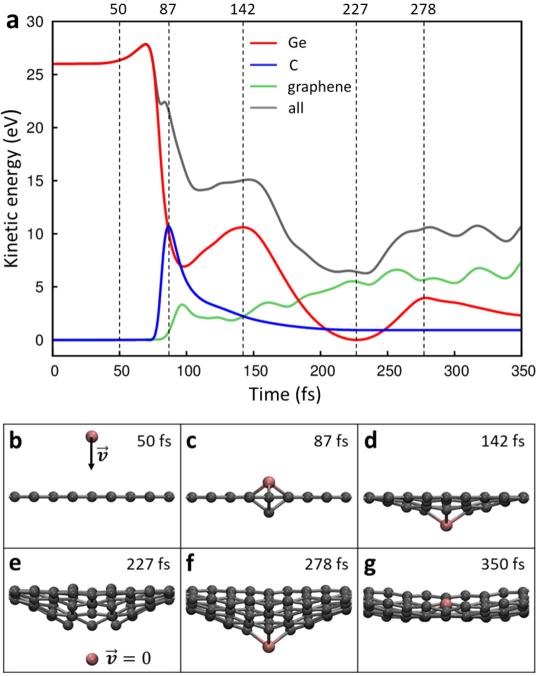
Interestingly, in simulations with higher energies, the long tail after the initial drop of starts to disappear. For example, for an initial Ge energy of 40 eV, becomes constant within 40 fs and decreases by only 5.7 eV from the maximum. This suggests that the C needs a kinetic energy of only about 5.7 eV to overcome the interaction with the graphene lattice after a head-on collision with Ge. The long tail in at low ion energies occurs mainly because of the interaction of C with the Ge ion, which can be considerable when both atoms are in close proximity and on the same side of graphene plane. At high values for the initial energies of the incident ion, the knocked-out C atom quickly moves away from graphene before the ion passes through the layer and therefore the tail in disappears.
Coming back to the example shown in Fig. 5, the Ge ion continues to move in the same direction after the collision and the amount of kinetic energy transferred to C atoms in the lattice increases. A minimum in at around 100 fs corresponds to the point when the ion passes through the graphene layer. The subsequent increase in occurs partially because the ion is moving towards a more energetically favourable configuration (Fig. 5d) and partially due to the interaction with the sputtered C atom. The energy increase is significantly smaller in simulations for higher ion energies, confirming that at low ion energies the Ge-C interaction plays an important role. The kinetic energy of the ion then goes to zero while gradually increases. Figure 5e shows the configuration at which equals zero. Although the ion has travelled a significant distance (about 4.3 Å) past the plane of graphene, the interaction with the highly buckled lattice is strong enough to stop and reverse the motion of the ion. The distance between the Ge and the undercoordinated C atoms at this time step is about 2.9 Å. Moving backwards, the ion gains enough kinetic energy to pass again through the graphene layer (Fig. 5f-g), before it finally stops, bound to the lattice. Further atomic motions in the system are relatively slow and do not involve significant structural rearrangements.
Finally, we should address the success of experimental implantation at energies below those predicted by our modeling. Considering the finite precision of the experimental ion energy, possible variation in the local bias potential, and the sources of inaccuracy in the simulations (including the approximation of exchange and correlation, the neglect of spin, and any basis set superposition error), as well as the simulated penetration of Ge into the lattice already between 20–22 eV, the modeling is actually surprisingly accurate. A statistical comparison of different experimental ion energies, as well as simulations covering the entire impact parameter space, would be required to make more precise direct comparisons.
Conclusion
We have implanted thus far the heaviest directly observed graphene impurity, and shown that despite its size, germanium can substitute a single atom by bonding to three carbon neighbors. Our first principles molecular dynamics simulations reveal that due to a strong chemical interaction between the incoming Ge ion and the neighbours of the displaced C atom, implantation can be carried out at an energy below the displacement threshold for graphene. As in earlier works, sample contamination remains an issue, and preventing it during implantation is an important target for improving sample quality in future experiments. Nevertheless, ion implantation continues to progress towards its promise as a scalable and precise technique for controllably doping 2D materials.
M.T. and T.S. acknowledge funding by the Austrian Science Fund (FWF) via project P 28322-N36 and J.K. via project I3181-N36. J.K. was also supported by the Wiener Wissenschafts-Forschungs- und Technologiefonds (WWTF) via project MA14-009. A.M. and E.B. acknowledge funding from the European Research Council under the European Union’s Seventh Framework Programme (FP7) / ERC grant agreement № 307755-FIN. We thank the technical staff of the ion beam center facility of HZDR Dresden for providing us with support and facilities for the ion implantation experiments. DFT-based molecular dynamics simulations were performed using the high performance computing facility at the University of Nottingham, and further simulations at the HPC Midlands Plus Centre and the Vienna Scientific Cluster (VSC).
Methods
Low-energy 74Ge+ ions were implanted at the HZDR ion beam center into commercially available monolayer graphene supported on Au TEM grids (QuantifoilⓇ R 2/4, Graphenea). We used a mass-selected, twofold electrostatic raster-scanned ion implantation system (Danfysik A/S, Denmark, Model 1050), providing ion energies down to 100 eV. Neutralized ions were eliminated by deflecting the 74Ge+ ion beam and then decelerating it towards the target. To reduce energies down to 15 eV, a bias voltage was set to the sample holder by an adjustable anode potential. The samples were irradiated in a 10-7 mbar vacuum at room temperature with a fluence of 1014 cm-2 (estimated with multiple Faraday cups). We chose ion energies of 15, 20 and 25 eV to minimize irradiation-induced damage. The amount of energy that can be transferred to a carbon atom due to a collision with such ions is below the experimentally estimated displacement threshold energy (21.14 eV) of graphene 34. Lower energies than expected are sufficient due to a strong chemical effect between the incoming Ge ion and the structure around the C atom being displaced. In an effort to reduce contamination 35, a 445 nm laser diode was aimed at the sample through a viewport of the vacuum chamber both for 2 min before implantation (nominal laser power 480 mW) and during the implantation (240 mW).
The samples were imaged in near ultra-high vacuum ( mbar) in an aberration-corrected Nion UltraSTEM100 scanning transmission electron microscope 36 operated at an acceleration voltage of 60 kV, well below the knock-on damage threshold of graphene 34. The beam current was around 50 pA, the beam convergence semi-angle was 30 mrad, and angular range was 60–200 mrad for MAADF and 80–300 mrad for HAADF. Some images were processed using a double Gaussian filtering procedure 37 and all colored with the ImageJ lookup table ”mpl-magma” to highlight relevant details. Low-loss EELS was recorded in the same instrument using a Gatan PEELS 666 spectrometer retrofitted with an Andor iXon 897 electron-multiplying charge-coupled device (EMCCD) camera 20. The energy dispersion was 0.1 eV/pixel (with an instrumental broadening of 0.4 eV) and the EELS collection semiangle was 35 mrad. Additionally, for greater sensitivity for Ge, we collected energy-dispersive x-ray spectra in a Philips CM200 TEM instrument operated at 80 kV.
To model the Ge substitution, we replaced one C atom in a 74 orthorhombic supercell of graphene (112 atoms in total), and relaxed its structure via DFT using the GPAW package 38 (PBE functional 39, 0.16 Å grid spacing, 551 Monkhorst-Pack k-points 40). The structure was used as input for a quantitative STEM simulation using the QSTEM software package 41, with scattering potentials generated from the independent atom model 42. The implantation of Ge was simulated using DFT-based molecular dynamics (MD) as implemented in the SIESTA code 43. We used Troullier-Martins norm-conserving pseudopotentials 44, the PBE functional, and a double- polarized basis set. The charge density was represented on a real-space grid with an energy cutoff of 300 Ry. For these simulations, graphene was modeled using orthorhombic supercells consisting of 160 carbon atoms. A vacuum layer of 20 Å was included in the direction normal to the graphene plane and the Brillouin zone was sampled using 331 k-points. To account for dispersion interactions, the Grimme semiempirical potential 45 was used. The time step in MD calculations was set to 0.5 fs and the initial kinetic energy of the Ge was varied at 1 eV intervals. Although we call them ions for convenience, note that the projectiles in the simulations are neutral atoms.
References
- Novoselov et al. 2004 Novoselov, K. S.; Geim, A. K.; Morozov, S. V.; Jiang, D.; Zhang, Y.; Dubonos, S. V.; Grigorieva, I. V.; Firsov, A. A. Electric Field Effect in Atomically Thin Carbon Films. Science 2004, 306, 666–669
- Balandin et al. 2008 Balandin, A. A.; Ghosh, S.; Bao, W.; Calizo, I.; Teweldebrhan, D.; Miao, F.; Lau, C. N. Superior Thermal Conductivity of Single-Layer Graphene. Nano Letters 2008, 8, 902–907
- Lee et al. 2008 Lee, C.; Wei, X.; Kysar, J. W.; Hone, J. Measurement of the Elastic Properties and Intrinsic Strength of Monolayer Graphene. Science 2008, 321, 385–388
- Bolotin et al. 2008 Bolotin, K.; Sikes, K.; Jiang, Z.; Klima, M.; Fudenberg, G.; Hone, J.; Kim, P.; Stormer, H. Ultrahigh electron mobility in suspended graphene. Solid State Communications 2008, 146, 351 – 355
- Guo et al. 2010 Guo, B.; Liu, Q.; Chen, E.; Zhu, H.; Fang, L.; Gong, J. R. Controllable N-Doping of Graphene. Nano Letters 2010, 10, 4975–4980
- Banhart et al. 2011 Banhart, F.; Kotakoski, J.; Krasheninnikov, A. V. Structural Defects in Graphene. ACS Nano 2011, 5, 26–41
- Ito et al. 2014 Ito, Y.; Christodoulou, C.; Nardi, M. V.; Koch, N.; Sachdev, H.; Müllen, K. Chemical Vapor Deposition of N-Doped Graphene and Carbon Films: The Role of Precursors and Gas Phase. ACS Nano 2014, 8, 3337–3346
- Persaud et al. 2004 Persaud, A.; Park, S. J.; Liddle, J. A.; Rangelow, I. W.; Bokor, J.; Keller, R.; Allen, F. I.; Schneider, D. H.; Schenkel, T. Quantum Computer Development with Single Ion Implantation. Quantum Information Processing 2004, 3, 233–245
- Åhlgren et al. 2011 Åhlgren, E. H.; Kotakoski, J.; Krasheninnikov, A. V. Atomistic simulations of the implantation of low-energy boron and nitrogen ions into graphene. Phys. Rev. B 2011, 83, 115424
- Lehtinen et al. 2015 Lehtinen, O.; Vats, N.; Algara-Siller, G.; Knyrim, P.; Kaiser, U. Implantation and Atomic-Scale Investigation of Self-Interstitials in Graphene. Nano Letters 2015, 15, 235–241
- Kotakoski et al. 2005 Kotakoski, J.; Krasheninnikov, A. V.; Ma, Y.; Foster, A. S.; Nordlund, K.; Nieminen, R. M. B and N ion implantation into carbon nanotubes: Insight from atomistic simulations. Phys. Rev. B 2005, 71, 205408
- Xu et al. 2007 Xu, F.; Minniti, M.; Giallombardo, C.; Cupolillo, A.; Barone, P.; Oliva, A.; Papagno, L. Nitrogen ion implantation in single wall carbon nanotubes. Surf. Sci. 2007, 601, 2819–2822
- Bangert et al. 2013 Bangert, U.; Pierce, W.; Kepaptsoglou, D. M.; Ramasse, Q.; Zan, R.; Gass, M. H.; Van den Berg, J. A.; Boothroyd, C. B.; Amani, J.; Hofsäss, H. Ion Implantation of Graphene—Toward IC Compatible Technologies. Nano Letters 2013, 13, 4902–4907
- Willke et al. 2015 Willke, P.; Amani, J. A.; Sinterhauf, A.; Thakur, S.; Kotzott, T.; Druga, T.; Weikert, S.; Maiti, K.; Hofsäss, H.; Wenderoth, M. Doping of Graphene by Low-Energy Ion Beam Implantation: Structural, Electronic, and Transport Properties. Nano Letters 2015, 15, 5110–5115
- Bangert et al. 2017 Bangert, U.; Stewart, A.; O’Connell, E.; Courtney, E.; Ramasse, Q.; Kepaptsoglou, D.; Hofsäss, H.; Amani, J.; Tu, J.-S.; Kardynal, B. Ion-beam modification of 2-D materials - single implant atom analysis via annular dark-field electron microscopy. Ultramicroscopy 2017, 176, 31 – 36
- Kepaptsoglou et al. 2015 Kepaptsoglou, D.; Hardcastle, T. P.; Seabourne, C. R.; Bangert, U.; Zan, R.; Amani, J. A.; Hofsäss, H.; Nicholls, R. J.; Brydson, R. M. D.; Scott, A. J. et al. Electronic Structure Modification of Ion Implanted Graphene: The Spectroscopic Signatures of p- and n-Type Doping. ACS Nano 2015, 9, 11398–11407
- Zhou et al. 2012 Zhou, W.; Kapetanakis, M. D.; Prange, M. P.; Pantelides, S. T.; Pennycook, S. J.; Idrobo, J.-C. Direct Determination of the Chemical Bonding of Individual Impurities in Graphene. Phys. Rev. Lett. 2012, 109, 206803
- Ramasse et al. 2013 Ramasse, Q. M.; Seabourne, C. R.; Kepaptsoglou, D.-M.; Zan, R.; Bangert, U.; Scott, A. J. Probing the Bonding and Electronic Structure of Single Atom Dopants in Graphene with Electron Energy Loss Spectroscopy. Nano Letters 2013, 13, 4989–4995
- Susi et al. 2017 Susi, T.; Meyer, J.; Kotakoski, J. Manipulating low-dimensional materials down to the level of single atoms with electron irradiation. Ultramicroscopy 2017, 180, 163–172
- Susi et al. 2017 Susi, T.; Hardcastle, T. P.; Hofsäss, H.; Mittelberger, A.; Pennycook, T. J.; Mangler, C.; Drummond-Brydson, R.; Scott, A. J.; Meyer, J. C.; Kotakoski, J. Single-atom spectroscopy of phosphorus dopants implanted into graphene. 2D Materials 2017, 4, 021013
- Ould Ne et al. 2017 Ould Ne, M. L.; Abbassi, A.; El hachimi, A. G.; Benyoussef, A.; Ez-Zahraouy, H.; El Kenz, A. Electronic optical, properties and widening band gap of graphene with Ge doping. Optical and Quantum Electronics 2017, 49, 218
- Nieman et al. 2017 Nieman, R.; Aquino, A. J. A.; Hardcastle, T. P.; Kotakoski, J.; Susi, T.; Lischka, H. Structure and electronic states of a graphene double vacancy with an embedded Si dopant. The Journal of Chemical Physics 2017, 147, 194702
- Denis 2014 Denis, P. A. Chemical Reactivity and Band-Gap Opening of Graphene Doped with Gallium, Germanium, Arsenic, and Selenium Atoms. ChemPhysChem 2014, 15, 3994–4000
- Eberlein et al. 2008 Eberlein, T.; Bangert, U.; Nair, R. R.; Jones, R.; Gass, M.; Bleloch, A. L.; Novoselov, K. S.; Geim, A.; Briddon, P. R. Plasmon spectroscopy of free-standing graphene films. Phys. Rev. B 2008, 77, 233406
- Krivanek et al. 2010 Krivanek, O. L.; Chisholm, M. F.; Nicolosi, V.; Pennycook, T. J.; Corbin, G. J.; Dellby, N.; Murfitt, M. F.; Own, C. S.; Szilagyi, Z. S.; Oxley, M. P. et al. Atom-by-atom structural and chemical analysis by annular dark-field electron microscopy. Nature 2010, 464, 571–574
- Zhou et al. 2012 Zhou, W.; Lee, J.; Nanda, J.; Pantelides, S. T.; Pennycook, S. J.; Idrobo, J.-C. Atomically localized plasmon enhancement in monolayer graphene. Nature Nanotechnology 2012, 7, 161–165
- Hage et al. 2018 Hage, F. S.; Hardcastle, T. P.; Gjerding, M. N.; Kepaptsoglou, D. M.; Seabourne, C. R.; Winther, K. T.; Zan, R.; Amani, J. A.; Hofsaess, H. C.; Bangert, U. et al. Local Plasmon Engineering in Doped Graphene. ACS Nano 2018, Article ASAP, 10.1021/acsnano.7b08650
- Gatan, Inc. 2018 Gatan, Inc., EELS Atlas. 2018; \urlhttp://www.eels.info/atlas
- Nguyen et al. 2012 Nguyen, P. D.; Kepaptsoglou, D. M.; Erni, R.; Ramasse, Q. M.; Olsen, A. Quantum confinement of volume plasmons and interband transitions in germanium nanocrystals. Phys. Rev. B 2012, 86, 245316
- Krivanek et al. 2014 Krivanek, O. L.; Lovejoy, T. C.; Dellby, N.; Aoki, T.; Carpenter, R. W.; Rez, P.; Soignard, E.; Zhu, J.; Batson, P. E.; Lagos, M. J. et al. Vibrational spectroscopy in the electron microscope. Nature 2014, 514, 209–212
- Lovejoy et al. 2012 Lovejoy, T. C.; Ramasse, Q. M.; Falke, M.; Kaeppel, A.; Terborg, R.; Zan, R.; Dellby, N.; Krivanek, O. L. Single atom identification by energy dispersive x-ray spectroscopy. Applied Physics Letters 2012, 100, 154101
- Susi et al. 2017 Susi, T.; Skákalová, V.; Mittelberger, A.; Kotrusz, P.; Hulman, M.; Pennycook, T. J.; Mangler, C.; Kotakoski, J.; Meyer, J. C. Computational insights and the observation of SiC nanograin assembly: towards 2D silicon carbide. Scientific Reports 2017, 7, 4399
- Susi et al. 2014 Susi, T.; Kotakoski, J.; Kepaptsoglou, D.; Mangler, C.; Lovejoy, T. C.; Krivanek, O. L.; Zan, R.; Bangert, U.; Ayala, P.; Meyer, J. C. et al. Silicon–Carbon Bond Inversions Driven by 60-keV Electrons in Graphene. Phys. Rev. Lett. 2014, 113, 115501
- Susi et al. 2016 Susi, T.; Hofer, C.; Argentero, G.; Leuthner, G. T.; Pennycook, T. J.; Mangler, C.; Meyer, J. C.; Kotakoski, J. Isotope analysis in the transmission electron microscope. Nature Communications 2016, 7, 13040
- Tripathi et al. 2017 Tripathi, M.; Mittelberger, A.; Mustonen, K.; Mangler, C.; Kotakoski, J.; Meyer, J. C.; Susi, T. Cleaning graphene: Comparing heat treatments in air and in vacuum. physica status solidi (RRL) 2017, 11, 1700124
- Krivanek et al. 2008 Krivanek, O. L.; Corbin, G. J.; Dellby, N.; Elston, B. F.; Keyse, R. J.; Murfitt, M. F.; Own, C. S.; Szilagyi, Z. S.; Woodruff, J. W. An electron microscope for the aberration-corrected era. Ultramicroscopy 2008, 108, 179–195
- Krivanek et al. 2010 Krivanek, O. L.; Dellby, N.; Murfitt, M. F.; Chisholm, M. F.; Pennycook, T. J.; Suenaga, K.; Nicolosi, V. Gentle STEM: ADF imaging and EELS at low primary energies. Ultramicroscopy 2010, 110, 935 – 945
- Enkovaara et al. 2010 Enkovaara, J.; Rostgaard, C.; Mortensen, J. J.; Chen, J.; Dulak, M.; Ferrighi, L.; Gavnholt, J.; Glinsvad, C.; Haikola, V.; Hansen, H. A. et al. Electronic structure calculations with GPAW: a real-space implementation of the projector augmented-wave method. J. Phys. Condens. Matter 2010, 22, 253202
- Perdew et al. 1996 Perdew, J. P.; Burke, K.; Ernzerhof, M. Generalized Gradient Approximation Made Simple. Phys. Rev. Lett. 1996, 77, 3865–3868
- Monkhorst and Pack 1976 Monkhorst, H. J.; Pack, J. D. Special points for Brillouin-zone integrations. Phys. Rev. B 1976, 13, 5188–5192
- Koch 2002 Koch, C. Determination of Core Structure Periodicity and Point Defect Density along Dislocations. Ph.D. thesis, Arizona State University, 2002
- Rez et al. 1994 Rez, D.; Rez, P.; Grant, I. Dirac–Fock calculations of X-ray scattering factors and contributions to the mean inner potential for electron scattering. Acta Crystallographica Section A Foundations of Crystallography 1994, 50, 481–497
- Soler et al. 2002 Soler, J. M.; Artacho, E.; Gale, J. D.; García, A.; Junquera, J.; Ordejón, P.; Sánchez-Portal, D. The SIESTA method for ab initio order-N materials simulation. Journal of Physics: Condensed Matter 2002, 14, 2745
- Troullier and Martins 1991 Troullier, N.; Martins, J. L. Efficient pseudopotentials for plane-wave calculations. II. Operators for fast iterative diagonalization. Phys. Rev. B 1991, 43, 8861–8869
- Grimme 2006 Grimme, S. Semiempirical GGA-type density functional constructed with a long-range dispersion correction. Journal of Computational Chemistry 2006, 27, 1787–1799