Beneficial impact of tunneling in nano-structured intermediate-band solar cell
Abstract
Using the non equilibrium Green functions formalism we propose a study of the electronic excitation and collection in nano-structured intermediate-band solar cell. We demonstrate that a thin tunnel barrier between the nano-objects and the host material is beneficial for both current and voltage. For the current, the confinement generated by such a thin barrier favors the intersubband optical coupling in the nano-objects and then improves the excitation-collection trade-off. We also show that a broaden density-of-state in the nano-objects increases the radiative recombination and then degrades the voltage. Using a detailed balance model we propose a broadening factor for this degradation which decreases when a tunnel barrier enhances the life-time in the nano-objects.
pacs:
Valid PACS appear hereI Introduction
By introducing an intermediate band (IB) in a wide bandgap solar cell, the aim is to increase the short-circuit current without reducing the open-circuit voltage Luque et al. (2012); Luque and Martí (1997). The current increases as the IB acts as a built-up converter to generate an electron-hole pair with two low-energy photons. To limit detrimental effect voltage drop, the IB must be electrically isolated from the contacts of the cell so that the recombination is still controlled by the wide bandgap. This theoretically allows to exceed the Shockley-Queisser (SQ) limit Shockley and Queisser (1961) with a controlled by the wide bandgap while low-energy photons generate electron-hole pairs.
Yet, practically, this concept has not yet resulted in a cell exceeding the SQ limit Sogabe et al. (2014); Okada et al. (2015). Worse, IB solar cell (IBSC), generally based on nano-objects, offers characteristics that are often lower than that of the same cells without IB Pusch et al. (2016). The small increase of current is not enough to catch up with the degradation of the . It is difficult to obtain a splitting between the Fermi levels of the IB and the contact (usually the n-type contact) because the electrons easily relax from the conduction band of the wide bandgap material to the IB. In other words, the IB is not well isolated from contacts and is controlled by recombination across a narrow bandgap.
Furthermore the increase of current remains low as it is difficult to have simultaneously an efficient photon absorption and a fast collection of the excited electrons. Indeed, if the IBSC is based on nano-objects, the electrons in IB are confined in localized states. The optical transition between the IB and the conduction band is then efficient if the excited state is also localized. This improves the wave-function overlap and the corresponding intraband (intersubband) transition Bastard (1988). However, if the excited electron is strongly confined in the nano-object, it cannot reach in the conduction band to be collected. It will finally relax by emitting photon and/or phonons. As a result the choice of the coupling between the excited state of the nano-objects and the conduction band of the wide bandgap is crucial to have a good excitation-collection trade-off. In case of bound-to-bound absorption with a thick tunnel barrier the absorption is high, but the electrons collection is limited. In a bound-to-continuum absorption without tunnel barrier the collection is fast but the absorption is low. In this letter we propose a comprehensive analysis of this problem. We will see that a thin tunneling barrier between the nano-object and the wide bandgap material offers a good excitation-collection trade-off. This permits to optimize the current. More unexpected, we will show that such a coupling also modifies the photon emission and then the .
II Model and system
This theoretical study is based on a quantum electronic transport model in the non equilibrium Green functions (NEGF) framework. This model allows to consider the quantum effects such as the confinement, the tunneling, the broadening due to the coupling and the scattering with the photons and the phonons. Nevertheless, except when this will be explicitly stated, we will not consider scattering with phonons. Such a radiative limit permits to facilitate the understanding of the results. The model used is described in Ref. Cavassilas et al. (2013) but as suggested in Ref. Cavassilas et al. (2016) we now consider the non-local character of the electron-photon interaction which guarantees compliance with the selection rules.
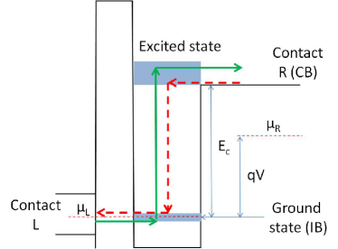
The modeled system is schematically shown Fig. 1. We consider a quantum well (QW) between two contacts. The left contact can only inject and collect electrons over an interval of 0.2 eV around the left Fermi level . The latter is located at the maximum of the density-of-states (DOS) of the ground state of the well. While this ground state mimics the IB, the corresponding Fermi level mimics the absorption between the valence band (no assumed in this work) and the IB. The electrons on this ground state can interact with photons and reach an excited state. From there, they either relax (and then do not participate in the current) or reach the right contact. This contact, located at an energy above , represents the conduction band-edge of the wide bandgap material. By reaching this contact the electrons generate a current that one chooses positive. The right contact can also inject electrons that can reach the QW, relax by emitting a photon and then reach the left contact. This behavior, which corresponds to the relaxation from conduction band to IB, generates a negative current which is all the more important as the right Fermi level is high. In an IBSC the aim is to have a positive current balance (more excitations than relaxations) while having a higher Fermi level in conduction band () than in IB (). Our system therefore behaves like an intraband solar cell under bias and characterized by a current and a voltage .
In the following we compare a bound-to-bound system in which a tunnel barrier is assumed between the QW and the right contact to a bound-to-continuum system in which we do not assume any barrier. While for an interband transition the definition of the energy gap seems obvious, this is not so trivial for an intraband-one. We defined the gap as the energy of the maximum absorption considering a black-body at 6000 K for the incident photon flux. For all systems assumed in this work, the gap is the same. We chose eV which is large compared to what is generally considered in IBSC. This choice is based on a study conducted elsewhere Delamarre et al. (2018) which shows that with a ratchet mechanism Pusch et al. (2016) of 0.7 eV, such a value is optimal in the case where the absorption is rather narrow as expected in intraband system. The other parameter is the effective mass which equals 0.665 (in free electron mass). Finally we chose to treat a QW since our one-dimensional model is well adapted to such a system. However, the physical behaviors such as confinement and absorption are very close in case of quantum dots. Moreover, if it is straigthforward to add a barrier between a QW and a contact, it is also feasible in case of quantum dots assuming a core-shell architecture Kim et al. (2005) or dots embedded in specific material (Sato et al., 2012). If in the present study we assume a QW, the conclusions can thus be easily extended to the quantum dots.
III Results
III.1 Current and voltage with the quantum model
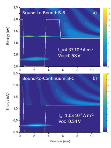
The band diagrams and the local-DOS of the two systems are represented in Fig. 2. In both the well thickness is 3.2 nm. In one case, the excited state is a localized state separated from the right contact by a 2 nm-thick tunnel barrier (Fig 2a). In this system, called bound-to-bound (B-B), equals 0.88 eV. In the other system the electrons are excited in an energy continuum directly connected to the right contact (Fig 2b). In the latter case, called bound-to-continuum (B-C), in order to have eV, is reduced to 0.855 eV. On Fig. 2 the LDOS clearly shows that in B-B the electrons are excited in a localized and narrow quantum state. In B-C, despite the absence of barrier, we do not obtain a true continuum but rather a strongly broadened state. Indeed, even without barrier, the QW involves quantum reflections and then interferences of the electronic wave-function.
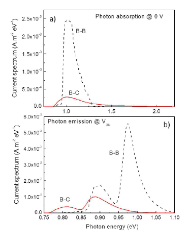
Regarding the results Fig. 2, and are both higher in B-B. In order to better understand this results, Fig. 3 shows the electronic current versus the photon energy for the two systems. The absorption spectra corresponds to the positive electronic current while the emission is the negative component. The absorption in B-B is narrower since, as shown in Fig. 2, the excited state is thinner. At same time this absorption is much higher than its the B-C counterpart. This can be explained by a better trade-off of the electronic collection and of the radiative excitation due to a larger wave-functions overlap in the bound-to-bound configuration. This explains that is larger in B-B despite the tunneling.
From the emission point of view, we obtain a lower bandgap in B-C. This behavior, which explains the degradation in B-C, may have several origins. In B-C, photons with lower energy are emitted since is lower. More relevant, due to tunneling in B-B, the emission of photon with low energy (between 0.78 and 0.85 eV) is reduced. But at that point, the origin of the lower emission bandgap in B-C is not yet clear.
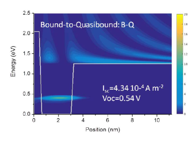
It is possible to improve B-C, for example, by reducing the thickness of the well (2.8 nm). This permits, as shown Fig. 4, to have a quasi-bound state narrower than the strongly broaden state of the B-C. In this new device, called B-Q, by adjusting at 0.88 eV in order to have eV, the current is largely higher than in the original B-C device, while is quite similar. Such a current increase is due to a better excitation-collection trade-off. However the current remains lower than in B-B. Moreover, the fact that in B-C and B-Q is close and lower than in B-B, confirms that is not simply controlled by . More generally such results suggest that a narrow excited state is better for both and . In the following, we propose to use a simpler model in order to verify and to explain this unintuitive feature.
III.2 Broadening factor in the detailed balance
We assume a detailed balance model where absorption and emission are calculated assuming a black-body distribution for the photons and a Lorentzian shape for the electronic DOS. Indeed, if we assume an homogeneous broadening due to contact (or others), the DOS spectral shape of states in the QW is given by a Lorentzian distribution Bastard (1988). If the tunneling between the excited state and the contact is low (large life-time ) the width of the Lorentzian is low following . We then apply this to the DOS of the exited state while, in order to simplify the model, the ground state is assumed as a Dirac function. We finally calculate the current, the emission and the voltage as:
| (1) | |||||
| (2) | |||||
| (3) |
with the black-body distribution
| (4) |
and the electronic joined DOS
| (5) |
where is the width, the energy of the maximum of the Lorentzian, the bias, the Boltzmann constant, and with the concentration factor. Note that for the integral of and the minimum of energy is given by the band-edge of the right contact. Finally and are respectively the temperature of the sun (6000 K) and of the cell (300 K). In this model the excitation-collection trade-off is not considered since , which represents the optical coupling, is taken as a constant and is directly given by the photon absorption in Eq. (1). This model is schematically described in Fig. 5.
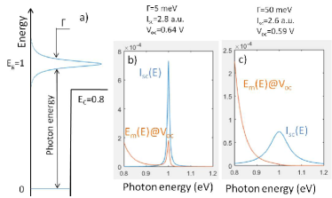
Figure 5 also shows the spectra and for two values of (5 and 50 meV) with eV and eV. As obtained with the NEGF model, and although this detailed balance model does not take into account the excitation-collection trade-off, we obtain both and larger with a thinner state. As shown Fig. 5, and are even more degraded than the DOS is high in the QW at the band-edge of the contact (). Indeed, a large means that a large proportion of excited electrons cannot be collected since their energy is lower that the band-edge of the contact. This degrades the current. A large also means a large electronic injection from the contact at low energy where the emission is very efficient. As already observed Fig. 3, this reduces the bandgap energy of the photon emission and then degrades the voltage. Such a behavior, as well as for example the reduction of the bandgap by tunneling in ultra thin cells Aeberhard and Rau (2017), shows that the electronic transport modifies the optical properties of nanoscale devices. With the detailed balance model we finally obtain this approximate expression for :
| (6) | |||||
with
| (7) | |||||
The two first terms in the expression of are the well-known Carnot and Boltzmann factors Markvart (2008); Hirst and Ekins-Daukes (2011) while the third one is relative to an original broadening behavior that we call the broadening factor. The origin of this degradation, as already observed in bulk materials Yao et al. (2015); Rau et al. (2017), is the mismatch between the absorption and the emission bandgaps. This factor is generally no considered in detailed balanced Markvart (2008) since the absorption is assumed sharp at the bandgap. In intraband system this broadening behavior degrades both and when the excited state is too thick like in the bound-to-continuum configuration.
Phonon emission is expected to favor the band-edge photon emission and then to degrade . With our NEGF model we show that such scattering with polar optical phonon is stronger in the continuum than in the QW (and is expected to be even weaker in quantum dot). The consequence is that scattering degrades in B-C (-90 mV) while this degradation is not significant in B-B. This result suggests that scattering with phonon increases the broadening factor. However this point deserves further investigations which cannot be conducted in the present work due to huge numerical burden.
III.3 Optimization of the tunnel barrier
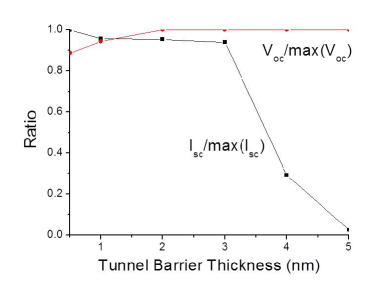
The broadening factor may suggest that in the B-B system better characteristics are expected if we assume a thick tunnel barrier between the nano-object and the contact. Indeed, due to strong tunnel reflection, life-time increases and then broadening of the excited state decreases. Fig. 6 shows the evolution of both and versus the tunnel barrier thickness in the B-B system (remember that in Fig. 2a, =2 nm). For lower than 2 nm, the reduction of is due to the broadening factor. At the same time the larger current with the ultra-thin barrier suggests another behavior like a reduction of the tunnel reflection improving the excitation-collection trade-off. This is confirmed for the thick barriers where and then the collection is strongly degraded by such a reflection. With a barrier thicker than 3 nm the excitation-collection trade-off is strongly degraded. In the same time, no more increases for barrier thicker than 2 nm since the excited state is thin enough ( meV) to cancel the broadening factor. For an optimal tunnel barrier both broadening factor and excitation-collection trade-off should be considered. With the parameters considered in this work the trade-off is optimal for a 2 nm-thick tunnel barrier. In case of an other material with an effective mass (in free electron mass) and a rectangular tunnel barrier offset (in eV), this tunneling coupling should be conserved if the thickness of the barrier (in nm) is given by .
IV Conclusion
We have shown that a broadening factor degrades the voltage in intraband system by improving the photon emission. To avoid this degradation a bound-to-bound system in which the electrons are collected by tunneling is well adapted. Moreover, such a thin tunnel barrier improves the excitation-collection trade-off due to a higher wave-function overlap. On the other hand a too thick tunnel barrier degrades this excitation-collection trade-off due to strong tunnel reflection. It is then necessary to choose a tunnel barrier thick enough to cancel the broadening factor and to improves the wave function overlap, but, thin enough to preserve the excitation-collection trade-off. We finally propose an equation allowing to calculate the thickness of the optimal barrier versus the effective mass and the tunnel barrier offset.
Acknowledgement
Nicolas Cavassilas and Daniel Suchet thank the Japan Society for the Promotion of Science (JSPS) for financial support.
References
- Luque et al. (2012) A. Luque, A. Martí, and C. Stanley, Nature Photonics 6, 146 (2012), ISSN 1749-4885, URL http://www.nature.com/nphoton/journal/v6/n3/full/nphoton.2012.1.html.
- Luque and Martí (1997) A. Luque and A. Martí, Physical Review Letters 78, 5014 (1997), URL https://link.aps.org/doi/10.1103/PhysRevLett.78.5014.
- Shockley and Queisser (1961) W. Shockley and H. J. Queisser, Journal of Applied Physics 32, 510 (1961), ISSN 0021-8979, URL http://aip.scitation.org/doi/abs/10.1063/1.1736034.
- Sogabe et al. (2014) T. Sogabe, Y. Shoji, M. Ohba, K. Yoshida, R. Tamaki, H.-F. Hong, C.-H. Wu, C.-T. Kuo, S. Tomić, and Y. Okada, Scientific Reports 4, srep04792 (2014), ISSN 2045-2322, URL https://www.nature.com/articles/srep04792.
- Okada et al. (2015) Y. Okada, N. J. Ekins-Daukes, T. Kita, R. Tamaki, M. Yoshida, A. Pusch, O. Hess, C. C. Phillips, D. J. Farrell, K. Yoshida, et al., Applied Physics Reviews 2, 021302 (2015), URL http://aip.scitation.org/doi/abs/10.1063/1.4916561.
- Pusch et al. (2016) A. Pusch, M. Yoshida, N. P. Hylton, A. Mellor, C. C. Phillips, O. Hess, and N. J. Ekins-Daukes, Progress in Photovoltaics: Research and Applications 24, 656 (2016), ISSN 1099-159X, URL http://onlinelibrary.wiley.com/doi/10.1002/pip.2751/abstract.
- Bastard (1988) G. Bastard, Wave mechanics applied to semiconductor heterostructures, Monographies de physique (Les Editions de Physique, 1988), ISBN 978-0-470-21708-5, URL https://books.google.fr/books?id=5rrvAAAAMAAJ.
- Cavassilas et al. (2013) N. Cavassilas, F. Michelini, and M. Bescond, Journal of Renewable and Sustainable Energy 6, 011203 (2013), URL http://aip.scitation.org/doi/abs/10.1063/1.4828366.
- Cavassilas et al. (2016) N. Cavassilas, F. Michelini, and M. Bescond, Journal of Computational Electronics 15, 1233 (2016), ISSN 1569-8025, 1572-8137, URL https://link.springer.com/article/10.1007/s10825-016-0883-5.
- Delamarre et al. (2018) A. Delamarre, D. Suchet, N. Cavassilas, Y. Okada, M. Sugiyama, and J.-F. Guillemoles, SPIE OPTO, To be published (2018).
- Kim et al. (2005) S.-W. Kim, J. P. Zimmer, S. Ohnishi, J. B. Tracy, J. V. Frangioni, and M. G. Bawendi, Journal of the American Chemical Society 127, 10526 (2005), ISSN 0002-7863, 1520-5126, URL http://pubs.acs.org/doi/abs/10.1021/ja0434331.
- Sato et al. (2012) D. Sato, J. Ota, K. Nishikawa, Y. Takeda, N. Miyashita, and Y. Okada, Journal of Applied Physics 112, 094305 (2012), ISSN 0021-8979, 1089-7550, URL http://aip.scitation.org/doi/10.1063/1.4764030.
- Aeberhard and Rau (2017) U. Aeberhard and U. Rau, Physical Review Letters 118, 247702 (2017), URL https://link.aps.org/doi/10.1103/PhysRevLett.118.247702.
- Markvart (2008) T. Markvart, physica status solidi (a) 205, 2752 (2008), ISSN 1862-6319, URL http://onlinelibrary.wiley.com/doi/10.1002/pssa.200880460/abstract.
- Hirst and Ekins-Daukes (2011) L. C. Hirst and N. J. Ekins-Daukes, Progress in Photovoltaics: Research and Applications 19, 286 (2011), ISSN 1099-159X, URL http://onlinelibrary.wiley.com/doi/10.1002/pip.1024/abstract.
- Yao et al. (2015) J. Yao, T. Kirchartz, M. S. Vezie, M. A. Faist, W. Gong, Z. He, H. Wu, J. Troughton, T. Watson, D. Bryant, et al., Physical Review Applied 4 (2015), ISSN 2331-7019, URL https://link.aps.org/doi/10.1103/PhysRevApplied.4.014020.
- Rau et al. (2017) U. Rau, B. Blank, T. C. Müller, and T. Kirchartz, Physical Review Applied 7 (2017), ISSN 2331-7019, URL http://link.aps.org/doi/10.1103/PhysRevApplied.7.044016.