Selective Area Grown Semiconductor-Superconductor Hybrids:
A Basis for Topological Networks
Abstract
We introduce selective area grown hybrid InAs/Al nanowires based on molecular beam epitaxy, allowing arbitrary semiconductor-superconductor networks containing loops and branches. Transport reveals a hard induced gap and unpoisoned 2e-periodic Coulomb blockade, with temperature dependent 1e features in agreement with theory. Coulomb peak spacing in parallel magnetic field displays overshoot, indicating an oscillating discrete near-zero subgap state consistent with device length. Finally, we investigate a loop network, finding strong spin-orbit coupling and a coherence length of several microns. These results demonstrate the potential of this platform for scalable topological networks among other applications.
Majorana zero modes (MZMs) at the ends of one-dimensional topological superconductors are expected to exhibit non-Abelian braiding statistics Kitaev2000 ; Read2000 , providing naturally fault-tolerant qubits Nayak2008 ; DasSarma2015 . Proposed realizations of braiding Alicea2011 ; Aasen2016 , interference-based topological qubits Flensberg2011 ; Plugge2017 ; Vijay2016 and topological quantum computing architectures Karzig2017 require scalable nanowire networks. While relatively simple branched or looped wires can be realized by specialized growth methods Gazibegovic2017 ; Krogstrup2015 or by etch- and gate-confined two-dimensional hybrid heterostructures Shabani2016 ; Kjaergaard2016 ; Suominen2017 ; Nichele2017 , selective area growth Krizek2018 enables deterministic patterning of arbitrarily complex structures. This allows complex continuous patterns of superconductor-semiconductor hybrids and topological networks.
Following initial theoretical proposals Lutchyn2010 ; Oreg2010 , a number of experiments have reported signatures of Majorana zero modes (MZMs) in hybrid semiconductor-superconductor nanowires Krogstrup2015 , including zero-bias conductance peaks Mourik2012 ; Das2012 ; Gul2018 ; Deng2016 ; Suominen2017 ; Nichele2017 ; Zhang2017 ; Deng2012 ; Sestoft2017 and Coulomb blockade peak spacing oscillations Albrecht2016 ; Sherman2016 . To date, experiments have used individual vapor-liquid-solid (VLS) nanowires Mourik2012 ; Das2012 ; Gul2018 ; Deng2016 ; Zhang2017 ; Deng2012 or gate-confined two-dimensional heterostructures Suominen2017 ; Nichele2017 . Within these approaches, constructing complex topological devices and networks containing branches and loops Alicea2011 ; Aasen2016 ; Flensberg2011 ; Vijay2016 ; Karzig2017 ; Plugge2017 is a challenge. Recently, branched and looped VLS growth has been developed toward this goal Krizek2017 ; Gazibegovic2017 .
In this Letter, we investigate a novel approach to the growth of semiconductor-superconductor hybrids that allows deterministic on-chip patterning of topological superconducting networks based on SAG. We characterize key physical properties required for building Majorana networks, including a hard superconducting gap, induced in the semiconductor, phase-coherence length of several microns, strong spin-orbit coupling, and Coulomb blockade peak motion compatible with interacting Majoranas. Overall, these properties show great promise for SAG-based topological networks.
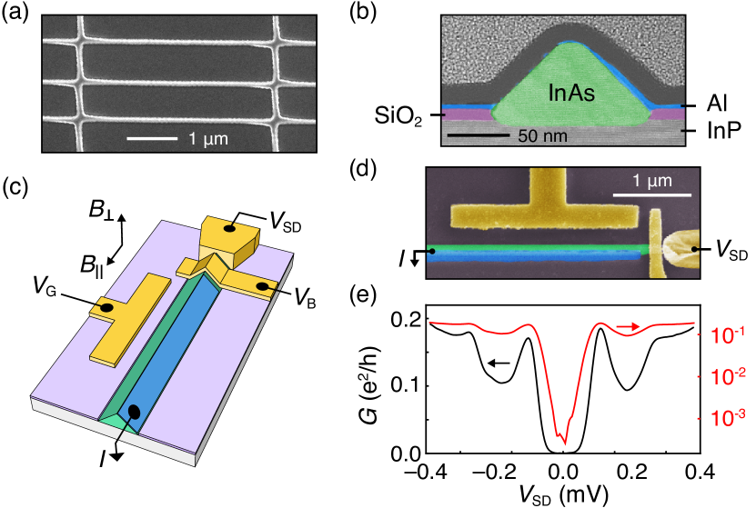
Selective area growth was realized on a semi-insulating InP substrate. PECVD grown SiOx was patterned using electron beam lithography and wet etching. InAs wires with triangular cross-sections were grown by molecular beam epitaxy (MBE). The Al was grown in-situ by MBE using angled deposition covering one of the facets. The excess Al was removed by wet etching [Fig. 1(a-c)]. The details of the semiconductor growth are given in Ref. Krizek2018 , while it is superconductor-semiconductor proximity effects that are emphasized in the present study. Data from four devices are presented. Device 1 [Fig. 1(d)] consists of a single barrier at the end of a wire, defined by a lithographically patterned gate adjacent to a Ti/Au contact where the Al has been removed by wet etching. This device allowed density of states measurement at the end of the wire by means of bias spectroscopy, to investigate the superconducting proximity effect in the InAs. Evolution of Coulomb blockade in temperature and magnetic field was studied in Device 2 [Fig. 2(b)]—a hybrid quantum dot with length of defined by two Ti/Au gates adjacent to etched-Al regions. The barrier voltages were used to create tunneling barriers. The chemical-potential in the wires was tuned with gate voltage . Device 3 was a micron-size square loop [Fig. 4(a)] with fully removed Al, which was used to extract phase coherence lengths from weak antilocalization (WAL) and Aharonov-Bohm (AB) oscillations. Device 4 [Fig. S 2 in the Supplemental Material SupMaterial ]—top-gated nanowire without Al—was used to extract the charge carrier mobility. The nanowires in Devices 1, 2 and 4 are parallel to direction, whereas the arms of Device 3 are oriented along and directions. Standard ac lock-in measurements were carried out in a dilution refrigerator with a three-axis vector magnet. See Supplemental Material SupMaterial for more detailed description of the growth, fabrication and measurement setup.
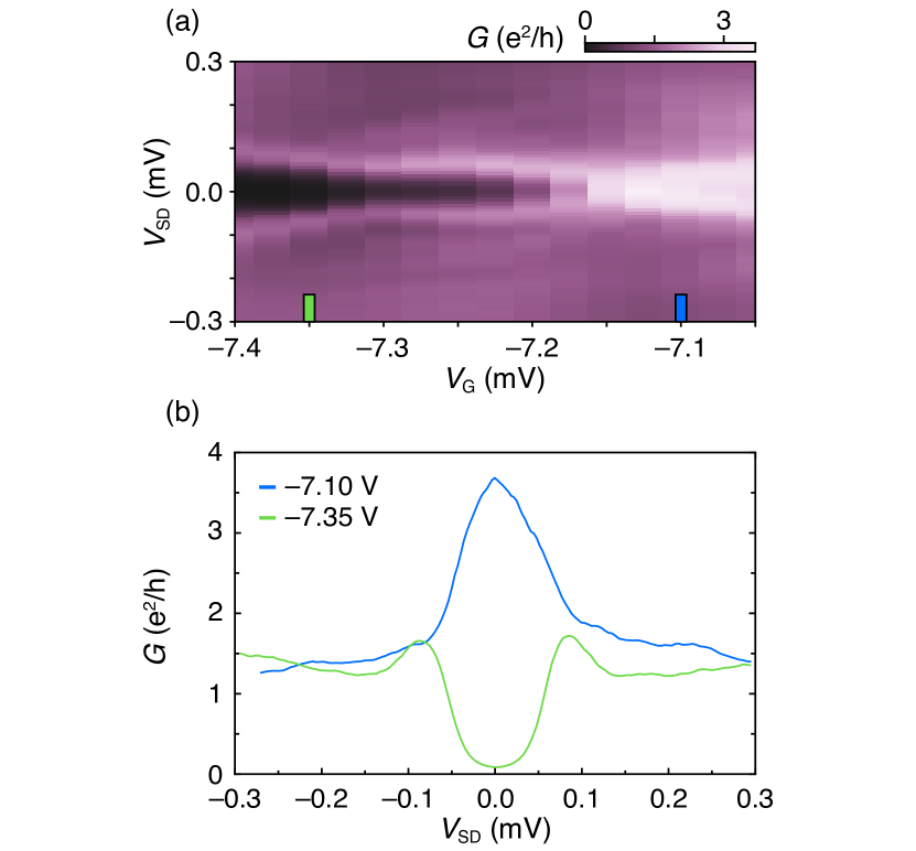
Differential conductance, , in the tunneling regime, as a function of source-drain bias, , for Device 1 [Fig. 1(e)] at reveals a gapped density of states with two peaks at and . We tentatively identify the two peaks with two populations of carriers in the semiconductor, the one with a larger gap residing at the InAs-Al interface and with a smaller at the InAs-InP. The magnitude of the larger superconducting gap is consistent with enhanced energy gaps of for Al film Court2008 . The zero-bias conductance is times lower than the above-gap conductance, a ratio exceeding VLS nanowire Chang2015 ; Gazibegovic2017 ; Zhang2017_2 and 2DEG devices Kjaergaard2016 , indicating a hard induced gap. We note, however, that co-tunneling through a quantum-dot or multichannel tunneling can enhance this ratio Beenakker1992 . The spectrum evolution with from enhanced to suppressed conductance around is shown in Fig. S 1 in Supplemental Material SupMaterial .
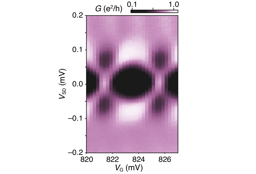
Transport through a Coulomb island geometry [Fig. 2] at low temperatures shows 2e-periodic peak spacing as a function of . Coulomb diamonds at finite bias yield a charging energy (see Fig. S1 in Supplemental Material SupMaterial ), smaller than the induced gap, , as seen in Fig. 1(e). The zero-bias Coulomb blockade spacing evolves to even-odd and finally to 1e-periodic peaks with increasing temperature, . The 2e to 1e transition in temperature does not result from the destruction of superconductivity, but rather arises due to the thermal excitation of quasiparticles on the island, as investigated previously in metallic islands Tuominen1992 ; Lafarge1993 and semiconductor-superconductor VLS nanowires Higginbotham2015 .
A thermodynamic analysis of Coulomb blockade peak spacings is based on the difference in free energies, , between even and odd occupied states. We consider a simple model that assumes a single induced gap , not accounting for the double-peaked density of states in Fig. 1(e). At low temperatures (), approaches . Above a characteristic poisoning temperature, , quasiparticles become thermally activated and decreases rapidly to zero. For , Coulomb peaks are 2e periodic with even peak spacings, , independent of . For , odd states become occupied, and the difference in peak spacing, , decreases roughly proportional to . A full analysis following Ref. Higginbotham2015 (see Supplemental Material SupMaterial ) yields the peak spacing difference
| (1) |
where is the dimensionless gate lever arm measured from Coulomb diamonds.
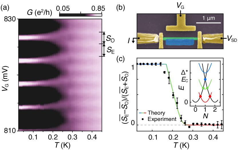
Figure 2(c) shows the measured even-odd difference in peak spacing, , averaged over 4 peaks in Device 2, along with Eq. (1). Thermodynamic analysis shows an excellent agreement with the peak spacing data across the full range of temperatures. The fit uses an independently measured , with the induced gap as a single fit parameter, yielding , a reasonable value that lies between the two density of states features in Fig. 1(e). The island remains unpoisoned below .
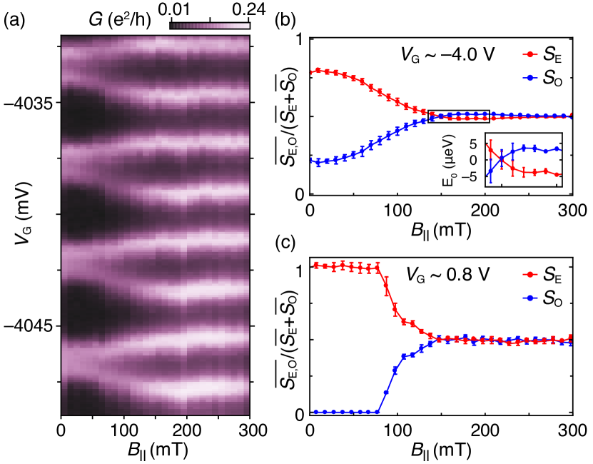
The evolution of Coulomb blockade peaks with parallel magnetic field, , is shown in Fig. 3(a). In this data set, peaks show even-odd periodicity at zero field due to a gate-dependent gap or a bound state at energy less than . A subgap state results in even-state spacing proportional to and odd-state spacing Albrecht2016 (see Supplemental Material SupMaterial ), giving
| (2) |
Figure 3(b) shows the dependence of even and odd peak spacings, , extracted from the data in Fig. 3(a), giving an effective -factor of . Even and odd peak spacings become equal at , then overshoot at higher fields with a maximum amplitude corresponding to . At more positive gate voltages [Fig. 3(c)], where the carrier density is higher, peaks are 2e-periodic at zero field, then transition through even-odd to 1e-periodic Coulomb blockade without an overshoot, with an effective -factor of .
Overshoot of peak spacing, with exceeding , indicates a discrete subgap state crossing zero energy Albrecht2016 ; Ciu2017 , consistent with interacting Majorana modes. The overshoot observed at more negative is quantitatively in agreement with the overshoot seen in VLS wires of comparable length Albrecht2016 . The absence of the overshoot and the increase of the -factor at positive is consistent with the gate-tunable carrier density in VLS wires Vaitiekenas2017 .
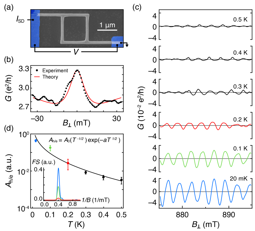
To demonstrate fabrication and operation of a simple SAG network, we investigate the coherence of electron transport in the loop structure shown in Fig. 4(a), with the Al layer completely removed by wet etching. Conductance as a function of perpendicular magnetic field, , shows a peak around zero magnetic field, characteristic of WAL [Fig. 4(b)]. A fit to a theoretical model for disordered quasi one-dimensional wires with strong spin-orbit coupling Kurdak1992 yields an electron phase-coherence length , and a spin-orbit length . We note that electrons propagating along and directions experience both Rashba and linear-Dresselhaus spin-orbit fields Sasaki2014 . The magnitude of each field can be deduced from a combination of in-plane magnetic field angle and magnitude dependence of the conductance correction due to the weak (anti-) localization. Such study, however, is out of scope of this work.
Upon suppressing WAL with a large perpendicular field periodic conductance oscillations are observed [Fig. 4(c)] with period corresponding to AB oscillations with area , matching the lithographic area of the loop. The oscillation amplitude, , measured from the power spectral band around [Fig. 4(d), inset] was observed to decrease with increasing temperature as seen in Fig. 4(d). The size of is dictated by two characteristic lengths–thermal length and phase-coherence length Kurdak1992 . We estimate at to be around using a charge carrier mobility and density (see Supplemental Material SupMaterial ). The thermal length is comparable to the loop circumference , as a result, energy averaging is expected to have finite contribution to the size of the conductance oscillations Kurdak1992 . Taking with and for a diffusive ring Ludwig2004 , a fit of the logarithmic amplitude yields and (Fig. 4d), giving a base-temperature phase-coherence length .
The discrepancy between the extracted and has previously been observed in an experiment on GaAs/AlGaAs-based arrays of micron-sized loops Ferrier2008 . It has been argued theoretically that WAL and AB interference processes are governed by different dephasing mechanisms Ludwig2004 . As a result, and have different temperature dependences.
Our results show that selective area grown hybrid nanowires are a promising platform for scalable Majorana networks exhibiting strong proximity effect. The hard induced superconducting gap and 2e-periodic Coulomb oscillations imply strongly suppressed quasiparticle poisoning. The overshoot of Coulomb peak spacing in a parallel magnetic field indicates the presence of a discrete low-energy state. Despite the relatively low charge carrier mobility, the measured SAG-based network exhibits strong spin-orbit coupling and phase-coherent transport. Furthermore, the ability to design hybrid wire planar structures containing many branches and loops—a requirement for realizing topological quantum information processing—is readily achievable in SAG. Future work on SAG-based hybrid networks will focus on spectroscopy, correlations, interferometry, and manipulation of MZMs.
We thank D. Carrad, A. Higginbotham and R. Lutchyn for valuable discussions as well as R. McNeil, C. Sørensen and S. Upadhyay for contributions to material growth and device fabrication. The research was supported by Microsoft, the Danish National Research Foundation, and the European Commission. C.M.M. acknowledges support from the Villum Foundation. M.T.D. acknowledges support from State Key Laboratory of High Performance Computing, China. S.M-S. acknowledges funding from ”Programa Internacional de Becas ”la Caixa”-Severo Ochoa”. ICN2 acknowledges support from the Severo Ochoa Programme (MINECO, Grant no. SEV-2013-0295) and is funded by the CERCA Programme / Generalitat de Catalunya. Part of the present work has been performed in the framework of Universitat Autònoma de Barcelona Materials Science PhD program.
References
- (1) A. Y. Kitaev, Physics-Uspekhi 131, 130-136 (2001).
- (2) N. Read, and D. Green, Phys. Rev. B 61, 10267 (2000).
- (3) C. Nayak, S. H. Simon, A. Stern, M. Freedman, and S. Das Sarma, Rev. Mod. Phys. 80, 1083 (2008).
- (4) S. Das Sarma, M. Freedman, and C. Nayak, NJP Quantum Information 1, 15001 (2015).
- (5) J. Alicea, Y. Oreg, G. Refael, F. von Oppen, and M. P. A. Fisher, Nat. Phys. 7, 412 (2011).
- (6) D. Aasen, Michael Hell, R. V. Mishmash, A. Higginbotham, J. Danon, M. Leijnse, T. S. Jespersen, J. A. Folk, C. M. Marcus, K. Flensberg, and J. Alicea, Phys. Rev. X 6, 031016 (2016).
- (7) K. Flensberg, Phys. Rev. Lett. 106, 090503 (2011).
- (8) S. Plugge, A. Rasmussen, R. Egger, and K. Flensberg, New J. Phys. 19, 012001 (2017).
- (9) S. Vijay, and L. Fu, Phys. Rev. B. 94, 235446 (2016).
- (10) T. Karzig, C. Knapp, R. M. Lutchyn, P. Bonderson, M. Hastings, C. Nayak, J. Alicea, K. Flensberg, S. Plugge, Y. Oreg, C. M. Marcus, and M. H. Freedman, Phys. Rev. B. 95, 235305 (2017).
- (11) P. Krogstrup, N. L. B. Ziino, W. Chang, S. M. Albrecht, M. H. Madsen, E. Johnson, J. Nygård, C. M. Marcus, and T. S. Jespersen, Nat. Mat. 14, 400 (2015).
- (12) S. Gazibegovic, D. Car, H. Zhang, S. C. Balk, J. A. Logan, M. W. A. de Moor, M. C. Cassidy, R. Schmits, D. Xu, G. Wang, P. Krogstrup, R. L. M. Op het Veld, K. Zuo, Y. Vos, J. Shen, D. Bouman, B. Shojaei, D. Pennachio, J. S. Lee, P. J. van Veldhoven, S. Koelling, M. A. Verheijen, L. P. Kouwenhoven, C. J. Palmstrøm, and E. P. A. M. Bakkers, Nature 548, 434 (2017).
- (13) J. Shabani, M. Kjaergaard, H. J. Suominen, Y. Kim, F. Nichele, K. Pakrouski, T. Stankevic, R. M. Lutchyn, P. Krogstrup, R. Feidenhans’l, S. Kraemer, C. Nayak, M. Troyer, C. M. Marcus, and C. J. Palmstrøm, Phys. Rev. B 93, 155402 (2016).
- (14) M. Kjaergaard, F. Nichele, H. J. Suominen, M. P. Nowak, M. Wimmer, A. R. Akhmerov, J. A. Folk, K. Flensberg, J. Shabani, C. J. Palmstrøm, and C. M. Marcus, Nat. Commun. 7, 12841 (2016).
- (15) H. J. Suominen, M. Kjaergaard, A. R. Hamilton, J. Sha- bani, C. J. Palmstrøm, C. M. Marcus, and F. Nichele, Phys. Rev. Lett. 119, 176805 (2017).
- (16) F. Nichele, A. C. C. Drachmann,1 A. M. Whiticar, E. C. T. O’Farrell,1 H. J. Suominen, A. Fornieri, T. Wang, G. C. Gardner, C. Thomas, A. T. Hatke, P. Krogstrup, M. J. Manfra, K. Flensberg, and C. M. Marcus, Phys. Rev. Lett. 119, 136803 (2017).
- (17) F. Krizek, J. E. Sestoft, P. Aseev, S. Marti-Sanchez, S. Vaitiekėnas, L. Casparis, S. A. Khan, Y. Liu, T. Stankevič, A. M. Whiticar, A. Fursina, F. Boekhout, R. Koops, E. Uccelli, L. P. Kouwenhoven, C. M. Marcus, J. Arbiol, P. Krogstrup, Phys. Rev. Materials 2, 093401 (2018).
- (18) R. Lutchyn, J. D. Sau, and S. Das Sarma, Phys. Rev. Lett. 105, 077001 (2010).
- (19) Y. Oreg, G. Refael, and F. von Oppen, Phys. Rev. Lett. 105, 177002 (2010).
- (20) V. Mourik, K. Zuo, S. M. Frolov, S. R. Plissard, E. P. A. M. Bakkers, and L. P. Kouwenhoven, Science 336, 1003 (2012).
- (21) M. T. Deng, C. L. Yu, G. Y. Huang, M. Larsson, P. Caroff, and H. Q. Xu, Nano Lett. 12, 6414 (2012).
- (22) A. Das, Y. Ronen, Y. Most, Y. Oreg, M. Heiblum, and H. Shtrikman, Nat. Phys. 8, 887 (2012).
- (23) Ö. Gül, H. Zhang, J. D. S. Bommer, M. W. A. de Moor, D. Car, S. R. Plissard, E. P. A. M. Bakkers, A. Geresdi, K. Watanabe, T. Taniguchi, and Leo P. Kouwenhoven, Nat. Nanotech. 13, 192 (2018).
- (24) M. T. Deng, S. Vaitiekėnas, E. B. Hansen, J. Danon, M. Leijnse, K. Flensberg, J. Nygård, P. Krogstrup, and C. M. Marcus, Science 354, 6319 (2016).
- (25) H. Zhang, C.-X. Liu, S. Gazibegovic, D. Xu, J. A. Logan, G. Wang, N. van Loo, J. D. S. Bommer, M. W. A. de Moor, D. Car, R. L. M. Op het Veld, P. J. van Veldhoven, S. Koelling, M. A. Verheijen, M. Pendharkar, D. J. Pennachio, B. Shojaei, J. S. Lee, C. J. Palmstrøm, E. P. A. M. Bakkers, S. Das Sarma, L. P. Kouwenhoven, Nature 556, 74 (2018).
- (26) J. E. Sestoft, T. Kanne, A. N. Gejl, M. von Soosten, J. S. Yodh, D. Sherman, B. Tarasinski, M. Wimmer, E. Johnson, M.-T. Deng, J. Nygård, T. S. Jespersen, C. M. Marcus, P. Krogstrup, Phys. Rev. Materials 2, 044202 (2018).
- (27) S. M. Albrecht, A. P. Higginbotham, M. Madsen, F. Kuemmeth, T. S. Jespersen, J. Nygård, P. Krogstrup, and C. M. Marcus, Nature 531, 7593 (2016).
- (28) D. Sherman, J. S. Yodh, S. M. Albrecht, J. Nygård, P. Krogstrup, and C. M. Marcus, Nat. Nanotechnol. 12 212 (2017).
- (29) F. Krizek, T. Kanne, D. Razmadze, E. Johnson, J. Nygård, C. M. Marcus, and P. Krogstrup, Nano Lett. 17, 6090 (2017).
- (30) See Supplemental Material for supporting information.
- (31) N. A. Court, A. J. Ferguson, and R. G. Clark, Supercond. Sci. Technol., 21, 015013 (2008).
- (32) W. Chang, S. M. Albrecht, T. S. Jespersen, F. Kuemmeth, P. Krogstrup, J. Nygård, and C. M. Marcus, Nat. Nanotechnol. 10, 232 (2015).
- (33) H. Zhang, Ö. Gül, S. Conesa-Boj, M. P. Nowak, M. Wimmer, K. Zuo, V. Mourik, F. K. de Vries, J. van Veen, M. W. A. de Moor, J. D. S. Bommer, D. J. van Woerkom, D. Car, S. R. Plissard, E. P. A. M. Bakkers, M. Quintero-Pérez, M. C. Cassidy, S. Koelling, S. Goswami, K. Watanabe, T. Taniguchi, and L. P. Kouwenhoven, Nat. Commun. 8, 16025 (2017).
- (34) C. W. J. Beenakker, Phys. Rev. B 46, 12841 (1992).
- (35) M. T. Tuominen, J. M. Hergenrother, T. S. Tighe, and M. Tinkham, Phys. Rev. Lett. 69, 1997 (1992).
- (36) P. Lafarge, P. Joyez, D. Esteve, C. Urbina, and M. H. Devoret, Phys. Rev. Lett. 70, 994 (1993).
- (37) A. P. Higginbotham, S. M. Albrecht, G. Kiršanskas, W. Chang, F. Kuemmeth, P. Krogstrup, T. S. Jespersen, J. Nygård, K. Flensberg, and C. M. Marcus, Nat. Phys. 11, 1017 (2015).
- (38) C.-K. Chiu, J. D. Sau, and S. Das Sarma, Phys. Rev. B. 96, 054504 (2017).
- (39) S. Vaitiekėnas, M.-T. Deng, J. Nygård, P. Krogstrup, and C. M. Marcus, Phys. Rev. Lett. 121, 037703 (2018).
- (40) C. Kurdak, A. Chang, A. Chin, and T. Chang, Phys. Rev. B. 46, 6846 (1992).
- (41) A. Sasaki, S. Nonaka, Y. Kunihashi, M. Kohda, T. Bauernfeind, T. Dollinger, and J. Nitta, Nat. Nanotechnol., 9, 703 (2014).
- (42) M. Ferrier, A. C. H. Rowe, S. Guéron, H. Bouchiat, C. Texier, and G. Montambaux, Phys. Rev. Lett. 100, 146802 (2008).
- (43) T. Ludwig and A. D. Mirlin, Phys. Rev. B. 69, 193306 (2004).
I Supplemental Material
II Sample Preparation
The InAs nanowires with triangular cross-sections were selectively grown by MBE along the and directions on a semi-insulating InP substrate with a pre-patterned () SiOx mask supKrizek2017_2 . A thin () layer of Al was grown in-situ at low temperatures on one facet by angled deposition, forming an epitaxial interface with InAs. For the fabrication of the devices, Al was selectively removed using electron-beam lithography and wet etch (Transene Al Etchant D, , ). Normal Ti/Al () ohmic contacts were deposited after in-situ Ar milling (RF ion source, , , ). A film of HfO2 () was applied via atomic layer deposition at before depositing Ti/Au () gate electrodes.
III Measurement Setup
The measurements were carried out with a lock-in amplifier at in a dilution refrigerator with a base temperature of . For voltage bias measurements, an ac signal with an amplitude of was applied to a sample through a homebuilt resistive voltage-divider , resulting in excitation. For current bias, we applied ac signal to a resistor in series with a sample giving excitation.
IV Spectrum Evolution with
Evolution of differential conductance, , as a function of source-drain bias, , with gate voltage, , for Device 1 [Fig. 1(c,d), main text] is illustrated in Fig. S 1(a). Conductance enhancement in the range of to is measured at [Fig. S 1(b)]. At more negative gate voltage the conductance gets suppressed in the same range of .
We interpret these features to arise due to a different tunnel barrier strengths tunned by the capacitively cross-coupled : At more positive , the tunneling barrier is more transparent, resulting in Andreev reflection enhanced conductance; At more negative , the transport is dominated by the single electron tunneling, reflecting the local density of states at the end of the wire supBlonder1982 . At the zero-bias conductance is enhanced beyond the factor of compared to high bias [Fig. S 1(b)]. We speculate that this is caused by an interfering transport mediated via multiple channels or a quantum dot supBeenakker1992 . A similar study of dependence was not possible presumably due to a too high concentration of disorder in the junction.
V Free Energy Model
The theoretical fit in Fig. 2(b) of the main text is based on a free energy model given by Eq. 1 in the main text, where the difference in free energy between odd and even occupied states is given by
| (S1) |
with the effective number of continuum states , where is the volume of the island and is the density of states at the Fermi energy supTuominen1992 . The fit was obtained by using , consistent with Fig. 2(a) in the main text, electron density of states supTuominen1992 and , measured from Coulomb diamonds [Fig. S 2], with as the single fit parameter.
VI Device Energy
Energy, , of a Coulomb blockaded device with electron occupancy, , as a function of normalized gate voltage, , can be defined as
| (S2) |
where is the charging energy, is the relative free energy and for even (odd) parity of the device, see Fig. 2(c) in the main text, inset. Charge degeneracy points can be extracted using Eq. (S2), from which we can deduce the normalized even and odd peak spacings in units of charge, , as
| (S3) |
The even and odd peak spacing difference in gate voltage is given by
| (S4) |
with the dimensionless lever arm .
Note that in the limit of zero temperature, is defined by the size of the induced gap, , or, if present, by the energy of a subgap state, .
VII Field Effect Mobility
Conductance of a nanowire channel as a function of gate voltage is given by
| (S5) |
where is the mobility, is the capacitance between the gate electrode and the wire, is the length of the channel, is the gate voltage and is the threshold voltage supGul2015 . By introducing transconductance, , the mobility can be expressed by
| (S6) |
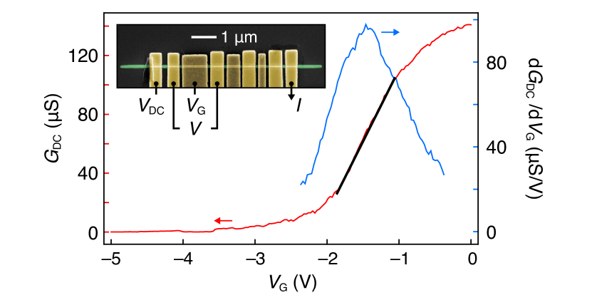
Conductance, , of Device 4 [Fig. S 3 inset] measured at and as a function of top-gate voltage, , is shown in Fig. S 3. The transconductance peaks to around , corresponding to the highest change in conductance indicated by the black line. The nanowire length is set by the distance between the contacts. The capacitance was estimated using COMSOL modeling software. Using Eq. S6 results in .
Measurements on a similar chemical beam epitaxy grown SAG Hall bar with comparable mobility result in charge carrier density of supCasparisUnpublished . The corresponding mean free path is
| (S7) |
where is the reduced Planck constant and is the elementary charge.
VIII Thermal Length
The size of the Aharonov-Bohm oscillations is dictated by two characteristic length scales, namely the phase-coherence and thermal lengths supKurdak1992 . The thermal length is related to the energy averaging of conduction channels due to the finite electron temperature and is given by
| (S8) |
where is the diffusion constant and is the Boltzmann constant. The diffusion constant is given by
| (S9) |
where is the Fermi velocity, with the Fermi wave vector and the effective electron mass in InAs , yielding , consistent with the values measured in vapor-liquid-solid (VLS) nanowires supJespersen2009 . The resulting thermal length is comparable to the loop circumference in Device 3 [Fig. 4(a), main text].
References
- (1) F. Krizek, J. E. Sestoft, P. Aseev, S. Marti-Sanchez, S. Vaitiekėnas, L. Casparis, S. A. Khan, Y. Liu, T. Stankevič, A. M. Whiticar, A. Fursina, F. Boekhout, R. Koops, E. Uccelli, L. P. Kouwenhoven, C. M. Marcus, J. Arbiol, P. Krogstrup, Phys. Rev. Materials 2, 093401 (2018).
- (2) G. E. Blonder, M. Tinkham, and T. Klapwijk, Phys. Rev. B 25, 4515 (1982).
- (3) C. W. J. Beenakker, Phys. Rev. B 46, 12841 (1992).
- (4) M. T. Tuominen, J. M. Hergenrother, T. S. Tighe, and M. Tinkham, Phys. Rev. Lett. 69, 1997 (1992).
- (5) Ö. Gül, D. J. van Woerkom, I. van Weperen, D. Car, S. R. Plissard, E. P. A. M. Bakkers, and L. P. Kouwenhoven, Nanotechnology 26, 215202 (2015).
- (6) L. Casparis, et al. (unpublished).
- (7) C. Kurdak, A. Chang, A. Chin, and T. Chang, Phys. Rev. B. 46, 6846 (1992).
- (8) T. S. Jespersen, M. L. Polianski, C. B. Sørensen, K. Flensberg, and J Nygård. New J. Phys. 11, 113025 (2009).