First-principles investigation of graphene/MoS2 bilayer heterostructures using Tkatchenko-Scheffler van der Waals method
Abstract
Graphene/MoS2 van der Waals (vdW) heterostructures have promising technological applications due to their unique properties and functionalities. Many experimental and theoretical research groups across the globe have made outstanding contributions to benchmark the properties of graphene/MoS2 heterostructures. Even though some research groups have already made an attempt to model the graphene/MoS2 heterostructures using first-principles calculations, there exists several discrepancies in the results from different theoretical research groups and the experimental findings. In the present work, we revisit this problem by first principles approach and address the existing discrepancies about the interlayer spacing between graphene and MoS2 monolayers in graphene/MoS2 heterostructures, and the location of Dirac points near Fermi-level. We find that the Tkatchenko–Scheffler method efficiently evaluates the long-range vdW interactions and accurately predicts interlayer spacing between graphene and MoS2 sheets. We further investigate the electronic, mechanical and vibrational properties of the optimized graphene/MoS2 heterostructures created using 55/44 and 44/33 supercell geometries having different magnitudes of lattice mismatch. The effect of the varying interlayer spacing on the electronic properties of heterostructures is discussed. Our phonon calculations reveal that the interlayer shear and breathing phonon modes, which are very sensitive to the weak vdW interactions, play vital role in describing the thermal properties of the studied systems. The thermodynamic and elastic properties of heterostructures are further discussed. A comparison between our results and the results reported from other research groups is presented.
I Introduction
The proximity of a substrate material is known to significantly change the electronic and optical properties of the widely celebrated graphene Novoselov et al. (2004, 2012); Castro Neto et al. (2009); Han et al. (2014); Novoselov et al. (2016); Singh et al. (2018a). Recently, this particular issue has been comprehensively investigated, both theoretically and experimentally, due to the promising applications of graphene-based van der Waals (vdW) heterostructures in the modern spintronics and optoelectronics industry Qian et al. (2015); Novoselov et al. (2016). The advanced material fabrication techniques have enabled us to stack different layers of materials in a controlled manner, and fabricate the desired vdW heterostructures for targeted applications. Graphene/MoS2 heterostructures are one of the most prominent vdW heterostructures that have been successfully synthesized in laboratory RadisavljevicB. et al. (2011); Roy et al. (2013); Bertolazzi et al. (2013); Sup Choi et al. (2013); Britnell et al. (2013); Larentis et al. (2014); Yu et al. (2014), and are proven to exhibit intriguing physical and chemical properties. Chhowalla et al. (2013); Yu et al. (2014) The presence of MoS2 substrate induces strong spin-orbit coupling (SOC) of strength 1 meV in graphene, which is almost 1000 times larger than the intrinsic SOC of pristine graphene, and consequently it opens a bandgap at Dirac point in graphene. Lu et al. (2014) Recent studies report the observation of exceptional optical response with large quantum efficiency, gate-tunable persistent photoconductivity, photocurrent generation, and negative compressibility in graphene/MoS2 heterostructures. Roy et al. (2013); Bertolazzi et al. (2013); Sup Choi et al. (2013); Britnell et al. (2013); Larentis et al. (2014); Yu et al. (2014) Electronic logic gates, memory devices, optical switches, energy conversion and storage devices, catalysts, and nanosensors have already been constructed using graphene/MoS2 heterostructures.Roy et al. (2013); Bertolazzi et al. (2013); Sup Choi et al. (2013); Britnell et al. (2013); Zhang et al. (2014); Larentis et al. (2014); Novoselov et al. (2016); Deng et al. (2016) Furthermore, graphene/MoS2 heterostructures intercalated with selected metals have been extensively investigated due to their extraordinary energy storage capacity and novel chemical properties. Chang et al. (2011); Chang and Chen (2011); Shao et al. (2015); Šljivančanin and Belić (2017)
Large lattice mismatch and presence of weak vdW interaction between graphene and MoS2 monolayers make the Density Functional Theory (DFT)Hohenberg and Kohn (1964); Kohn and Sham (1965) modeling of graphene/MoS2 heterostructures computationally challenging. Although the lattice mismatch can be minimized by stacking commensurate supercells of graphene and MoS2 monolayers, the correct first-principles determination of weak non-local vdW interactions remains elusive in graphene/MoS2 heterostructures. Various different methods have been employed to predict the correct interlayer spacing between graphene and MoS2 monolayers. Using the semiempirical DFT-D2 method of Grimme Grimme (2006) and 44/33 (hereafter 4:3) supercell geometry of graphene/MoS2, Gmitra et al. Gmitra and Fabian (2015) have predicted the interlayer spacing of 3.37 Å. They also observed that the Dirac point of graphene is located close to the conduction band of MoS2 indicating the enhanced screening and substantial increase in the mean free path of carriers in the graphene layer. Gmitra and Fabian (2015) Moreover, for the first time Gmitra et al. Gmitra and Fabian (2015) theoretically demonstrated the use of graphene/MoS2 heterostructures as a platform for optospintronic devices. Ebnonnasir et al. Ebnonnasir et al. (2014) studied two commensurate graphene/MoS2 bilayer heterostructures constructed using 55/44 (hereafter 5:4) and 44/33 supercells of graphene/MoS2. Using the vdW exchange-correlation functional of Klimeš et al. Klimeš et al. (2011) (optB86b-vdW), they predict the interlayer spacing of 3.11 and 3.13 Å for 5:4 and 4:3 heterostructure systems, respectively. Contrary to the report of Gmitra et al.Gmitra and Fabian (2015), the Dirac point in ref. Ebnonnasir et al. (2014) lies at the Fermi-level for 5:4 geometry and slightly above the Fermi-level for 4:3 geometry. Shao et al. Shao et al. (2015) reported an interlayer spacing of 3.37 Å for graphene/MoS2 4:3 bilayer system treated with Klimeš et al. Klimeš et al. (2011) vdW functional. They found that the Dirac point is located near the conduction band of MoS2 yet it is within the energy bandgap region. Li et al. Li et al. (2013a) reported an interlayer spacing of 3.36 Å for 4:3 graphene/MoS2 bilayer, they also report that the Dirac point is located above the Fermi-level touching the conduction band of MoS2 and therefore, indicating charge transfer between graphene and MoS2 layers as reported by Gmitra et al. Gmitra and Fabian (2015)
Using different ab-initio codes and different implementation for vdW corrections, several theoretically studies predicted graphene/MoS2 interlayer spacing ranging from 3.11 to 4.32 Å [see supplemental information (SI)] Ma et al. (2011); Ebnonnasir et al. (2014); Shao et al. (2015); Gmitra and Fabian (2015); Le et al. (2016); Hu et al. (2016); Šljivančanin and Belić (2017); Nguyen (2018). Also, different works inconsistently report distinct location of the Dirac point near Fermi-level and incoherently argue about the charge transfer mechanism in this system. However, the experimental investigations on graphene/MoS2 bilayer systems reveal an interlayer spacing of 3.40 0.1 Å and suggest no charge transfer between the layers at equilibrium conditions.Pierucci et al. (2016) Furthermore, although the vibrational, elastic and mechanical properties of pristine graphene and MoS2 monolayers have been thoroughly studied, Yan et al. (2008); Sofo et al. (2007); Wang et al. (2009); Lui and Heinz (2013); Ding et al. (2011); Zhao et al. (2013); Jiang et al. (2015); Tohei et al. (2006); Yuan et al. (2015); Lee et al. (2008); Cooper et al. (2013); Jiang (2015); Andrew et al. (2012); Wei et al. (2009); Liu et al. (2014); Peng and De (2013) a little attention has been paid to the aforementioned properties of their heterostructures.Le et al. (2016); Liu et al. (2014)
In this work, we revisit the problem of accurate evaluation of weak non-local vdW interactions in graphene/MoS2 bilayer heterostructures using different methodologies. We find that the DFT-D2 Grimme (2006) and Tkatchenko–Scheffler (DFT-TS) Tkatchenko and Scheffler (2009) methods yield very good estimate of the interlayer spacing in graphene/MoS2 bilayer heterostructure. We further present a detailed characterization of the electronic and vibrational (phonons) properties of the graphene/MoS2 heterostructures using DFT-TS method. We have studied the two most commonly used 5:4 and 4:3 supercell geometries of graphene/MoS2 heterostructures. To resolve the noted discrepancy about the location of Dirac point in the energy space, the effect of varying interlayer spacing on the electronic properties of graphene/MoS2 heterostructures is investigated. Our results indicate that the heat capacity and overall elastic properties of graphene/MoS2 heterostructures are considerably better compared to that of the individual monolayers.
II Computational Details
Density Functional Theory (DFT) Hohenberg and Kohn (1964); Kohn and Sham (1965) based first-principles calculations were carried out using the projector augmented-wave (PAW) method as implemented in the VASP code Kresse and Furthmüller (1996); Kresse and Joubert (1999), using the Perdew-Burke-Ernzerhof (PBE) parametrized generalized gradient approximation (GGA) exchange-correlation functional.Perdew et al. (1996) The SOC was employed by a second-variation method implemented in the VASP code. We considered twelve valence electrons of Mo (4, 5, 4), six valence electrons of S (3, 3), and four valence electrons of C (2, 2) in the PAW pseudo-potential. We consider two commensurate supercell geometries: (i) 5:4 and (ii) 4:3, to minimize the lattice mismatch between graphene and MoS2 layers. A vacuum of thickness larger than 17 Å was added along -axis to avoid the periodic interactions. The lattice parameters and the inner coordinates of atoms were optimized until the Hellmann-Feynman residual forces were less than eV/Å per atom, and eV was defined as the total energy difference criterion for convergence of electronic self-consistent calculations. SOC and vdW interactions (DFT-TS) Tkatchenko and Scheffler (2009); Bučko et al. (2013) were included in the structural optimization. We used eV as the kinetic energy cutoff of plane wave basis set and a -type -point mesh was employed to sample the irreducible Brillouin zone of heterostructures. The phonon calculations were performed using density functional perturbation theory (DFPT) approach, and PHONOPY code Togo et al. (2008) was used for the post-processing of data. To investigate the effect of uniaxial stress along -axis, we varied the interlayer spacing from (compression) to (expansion). The inner coordinates of all atoms in the strained cell were relaxed only along directions while maintaining their coordinates frozen. The PyProcar codeRomero and Munoz (2015); Singh et al. (2016a, b) was used to plot the spin-projected electronic bands, and the MechElastic scriptSingh and Romero (2017a) was used to evaluate the elastic properties of graphene/MoS2 bilayer heterostructures.
Complementary calculations were performed using ABINITGonze et al. (2016) code in order to guarantee that some of the observed physical properties are independent of the details of the numerical implementation and the approximations made to account for core electrons. In particular, the interlayer distance for 5:4 bilayer heterostructure and its corresponding band structure were evaluated. In order to calculate the interlayer equilibrium distance we performed DFT-D3 calculationsGrimme et al. (2010) omitting three-body contributions to the vdW energy Van Troeye et al. (2016). Terms involving two-atoms were taken into account for vdW correction if their energy contribution was larger than eV. The exchange-correlation functional used in ABINIT was chosen to be same as the one used in VASP calculations, however the criterion for convergence of the electronic self-consistent calculations was eV, and the plane wave cutoff was 980 eV. Optimized norm-conserving Vanderbilt pseudopotentials Hamann (2013) from the PseudoDojo van Setten et al. (2017) were used. The number of valence electrons for S and C atoms was same as mentioned earlier, while for Mo we considered 14 electrons (4, 4, 5, 4). No SOC was considered in the ABINIT calculations.
III Results and discussion
In the following sections, we present our results addressing the structural, electronic, vibrational, and elastic properties of graphene/MoS2 bilayers.
III.1 Crystal structure of graphene/MoS2 vdW heterostructures: Evaluation of the accurate vdW interaction
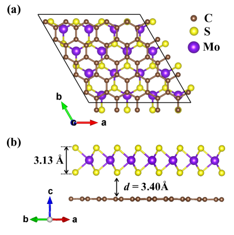
Figure 1 shows the crystal structure of 5:4 graphene/MoS2 bilayer heterostructure from two different crystal orientations. Since the 5:4 supercell geometry has lower lattice mismatch compared to that of the 4:3 combination, we decide to discuss the optimized crystal details for the 5:4 geometry here, however, details of the 4:3 structure are given in Table 1. The lattice parameters of SOC+vdW optimized 5:4 bilayer heterostructure are 12.443 Å. In this case, MoS2 sheet is being compressed by 0.3%, whereas the graphene sheet is being stretched by 1.16% from the optimized pristine cell parameters. Mo-S bond length is 2.38 Å and C-C bond length is 1.44 Å. The thickness of the MoS2 monolayer, i.e. the vertical distance between S-S planes, is 3.13 Å. The interlayer spacing () between graphene and MoS2 sheets is 3.40 Å, which is in excellent agreement with the experimentally reported interlayer spacing of 3.40 Å. Pierucci et al. (2016) However, the interlayer spacing () for 4:3 supercell geometry is 3.42 Å, which is slightly larger than the case of 5:4 geometry. This can be ascribed to the relatively large lattice mismatch between graphene and MoS2 monolayers in 4:3 geometry. On the other hand, DFT-D3 structural optimization in ABINIT yields very similar intralayer bond lenghts, while it underestimates the interlayer spacing. The latter was found to be 3.3 Å. Therefore, it is worth to note that the DFT-TS method Tkatchenko and Scheffler (2009); Bučko et al. (2013) remarkably describes the weak vdW interactions accurately in the graphene/MoS2 bilayers, whereas other semiempirical vdW methods Grimme (2006); Grimme et al. (2010); Klimeš et al. (2011); Lebedeva et al. (2017) appear to be not as accurate in describing this system.
The main reason behind the success of the DFT-TS method compared to the other vdW methods is the fact that the studied heterostructures consist of semimetallic and semi-insulating monolayers, thus having a large variation in the local charge density distribution at the interface (see Fig. 6). Formally, the TS-method is similar to the semiempirical DFT-D2 method of Grimme Grimme (2006). The key difference between these methods is that the vdW parameters, dispersion coefficients () and the damping function that scale the force field in vdW systems, are fixed for each element in DFT-D2 method and thus, these parameters are insensitive to the chemical environment of the system. Here, and refer to the atomic indices. For instance, the parameter for carbon atom in methane, diamond and graphene takes exactly same values. On the other hand, in the DFT-TS method vdW parameters, and are charge-density dependent. Therefore, the DFT-TS method is sensitive to the chemical environment. Since the DFT-TS method relies on the summation of the coefficients, derived from the electronic density of atoms in solid, and accurate reference data for free atom, the DFT-TS method efficiently accounts variations in vdW contribution of atoms due to their local chemical environment. In this method, polarizability (), and atomic radii of atom are calculated using the following relations:
| (1) |
| (2) |
| (3) |
The , and parameters for free atoms are taken from the reference data and effective atomic volumes are determined using the Hirshfeld partitioning of the all-electron density: Hirshfeld (1971)
| (4) |
Here, is the total electron density, is the spherically averaged electron density of the neutral free atomic species , and is the Hirshfeld weight.Hirshfeld (1971)
The optimized vdW parameters for graphene/MoS2 bilayer heterostructures are listed in Table 1. The cutoff radius for pairing interactions was set to 30 Å and the damping parameters and the reference data for free atomic species were used as implemented in the VASP code. For more technical details of the used methodology and application of the TS-method for dispersion corrections to DFT energies and forces to extended systems including noble-gas solids, molecular crystals, layered and chain-like structures, ionic crystals, and metals, we refer the reader to the excellent paper by Bučko et al.Bučko et al. (2013)
System bond length lattice parameters 5:4 heterostructure Mo: 1040.3 Mo: 4.1 Mo: 88.9 3.40 Mo-S bond = 2.38 = = 12.443 S: 129.3 S: 3.8 S: 19.3 C-C bond = 1.44 C: 35 C: 3.4 C: 10.4 S-S bond = 3.13 4:3 heterostructure Mo: 1036.7 Mo: 4.1 Mo: 88.8 3.42 Mo-S bond = 2.42 = = 9.698 S: 129.0 S: 3.8 S: 19.2 C-C bond = 1.40 C: 34.2 C: 3.4 C: 10.3 S-S bond = 3.08
III.2 Electronic structure
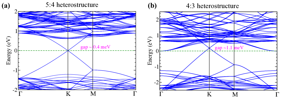
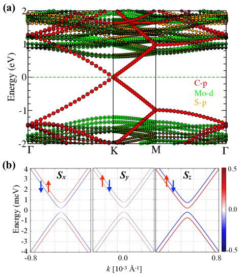
Figure 2 shows the electronic bandstructure of 5:4 and 4:3 graphene/MoS2 bilayers. The orbital projected electronic bandstructure for 5:4 bilayer heterostructure is given in Fig. 3(a). The orbitals character of electronic bands of graphene and MoS2 monolayer are well preserved in 5:4 bilayer heterostructure. In Fig. 3, one can notice that the electronic bands forming Dirac cone are coming from C- orbitals, whereas the other conduction and valence bands near Fermi-level are mainly composed of Mo- and S- orbitals. The direct bandgap between the conduction band minima and valence band maxima of MoS2 at K-point is 1.8 eV, which is in excellent agreement with reported values in the literature. Ramasubramaniam (2012); Espejo et al. (2013); Ebnonnasir et al. (2014); Amin et al. (2015); Ouma et al. (2017) Dirac point in 5:4 graphene/MoS2 bilayer is located at the Fermi-level and is well-separated from the conduction and valence bands of MoS2, which is in agreement with the experimental observations reporting no charge transfer between the layers at equilibrium conditions.Pierucci et al. (2016) The conduction and valence bands forming Dirac cone come from the A and B sublattices of graphene, respectively.
The SOC and proximity effects open a direct bandgap in graphene of 0.4 meV. In addition to open a direct bandgap at Dirac point, these effects also yield a parabolic shape to the linear bands near K-point. An enlarged view of spin-splitting of bands near K-point is shown in Fig. 3(b). Some notable features of the parabolic bands near K-point are: (i) Rashba spin-splitting due to the broken inversion symmetry and SOC effects from MoS2 layer, (ii) opening of a spin gap and anticrossing of bands due to the intrinsic SOC of graphene, and (iii) opening of an orbital gap due to the effective staggered potential arising from the proximity of MoS2 layer. Gmitra et al. (2009); Konschuh et al. (2010); Gmitra et al. (2017) A recent studyAlsharari et al. (2016) shows that a topological phase transition mediated by band-inversion at K-point can be achieved by utilizing an interlink among the aforementioned competitive interactions. In particular, the competition between the SOC effects from Mo- orbitals and the intrinsic SOC of graphene when combined with the staggered potential results in topologically distinct regimes where the bilayer heterostructure changes phase from a quantum spin Hall insulator to a normal insulator. In principle, these phases can be controlled by applying a relative gate voltage between the layers.Alsharari et al. (2016) Interestingly, in graphene/WSe2 bilayer heterostructure the band-inversion at Dirac point occurs naturally, thanks to the strong SOC of WSe2 layer, indicating presence of a non-trivial topological phase in graphene/WSe2 bilayer. Gmitra et al. (2016); Gmitra and Fabian (2017); Gmitra et al. (2017)
The direct bandgap at K-point increases almost by three times (from 0.4 meV to 1.1 meV) in the 4:3 graphene/MoS2 bilayer heterostructure. This can be partially attributed to the fact that the 4:3 bilayer inherits larger lattice mismatch compared to that of the 5:4 bilayer, and the interfacial strains often cause variation in the bandgap. Another interesting feature that we observe in 4:3 heterostructure is the charge-transfer between the layers. We notice that the Dirac point of graphene in 4:3 heterostructure is shifted above the lowest conduction band of MoS2, thus indicating donation of electrons to the MoS2 layer by graphene [see Fig. 2(b)]. Also, the valence and conduction bands of MoS2 layer are shifted towards lower energies in 4:3 heterostructure. The tunability of Dirac point and the charge-transfer process between the layers are of central interest for practical applications. Han et al. (2014); Roy et al. (2013)
Notably, MoS2 undergoes a direct to indirect bandgap transition in 4:3 bilayer heterostructure as can be seen in Fig. 2, while the direct bandgap characteristic of the isolated MoS2 monolayer is preserved in the 5:4 bilayer. Change from direct to indirect bandgap is observed even with just two layers of MoS2 without introducing any strain effects. Splendiani et al. (2010); Naik and Jain (2017) A recent work investigated the physical origin of layer dependence in bandstructure of two-dimensional materials, and concluded that in addition to the quantum confinement effects, the nonlinearity of exchange-correlation functional plays a crucial role in determining the direct to indirect bandgap transition in two-dimensional materials.Naik and Jain (2017) In case of the graphene/MoS2 bilayer having minimal strain i.e. the 5:4 bilayer, the gap transition is not present which indicates that the electronic interactions between graphene and MoS2 layer in 5:4 bilayer are subtler than that of in pristine MoS2 bilayer, and hence the transition in the 4:3 bilayer is triggered by the imposed strain to the layers. This finding is important since it suggests that the MoS2 monolayer supported on graphene can present high photoluminescence as it was previously found on samples supported on SiO2 Splendiani et al. (2010), and described theoretically in reference.Su et al. (2017) The electronic bandstructures calculated for graphene/MoS2 bilayers using ABINITGonze et al. (2016) code further corroborate this finding.
Based on the comparative analysis of 5:4 and 4:3 bilayer heterostructures, we argue that the existing controversy regarding the electronic bandstructure could be due to the inadequate evaluation of weak non-local vdW effects in these semi-metallic/semi-insulating heterostructures, and different lattice mismatches that were considered in the independently reported studies. Since the effect of biaxial strain, stacking order, and interlayer twist on the electronic structure of bilayer heterostructures has already been reported in the literature, Li et al. (2013b); Coy Diaz et al. (2015); Wang et al. (2015); Oakes et al. (2016); Pandey et al. (2016); Liu et al. (2016); Liu and Li (2015); Xu et al. (2017) in this work we investigate the effect of uniaxial stress along -axis on the electronic bandstructure of graphene/MoS2 bilayer heterostructures.
Effect of interlayer spacing on the electronic bandstructure: The effect of interlayer spacing on the electronic structure of the 5:4 bilayer heterostructure was studied by performing electronic bandstructure calculations at four values of interlayer strains, namely = -4%, -2%, +2%, and +4%, where positive (negative) values refer to expansion (compression) from the equilibrium interlayer distance. Atoms were allowed to relax in the plane of layers while their vertical coordinates were kept fixed at each separation. Figure 4 displays the bands (calculated with SOC) corresponding to the four upper valence bands and the four lower conduction bands near Fermi-level, for separations corresponding to 4% expansion (blue) and 4% compression (red) with respect to the equilibrium interlayer distance. The effect of diminishing interlayer distance is that the Mo bands shift to higher energy values with respect to the Fermi level. Since the increment is same for conduction and valence bands, the direct bandgap of MoS2 monolayer is not modified, as can be seen in Fig. 4. At point of Brillouin zone there is a spin splitting of Mo valence bands, which is depicted by arrows in Fig. 4. Such spin splitting is also present in the Mo conduction bands, however at point the conduction bands maintain the spin-degeneracy. The spin splitting of Mo valence bands is 0.2 eV, which remains constant in the range of studied interlayer separations.
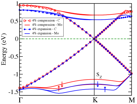
Regarding variation in the direct bandgap at Dirac point, we find that the gap at Dirac point increases substantially from 0.2 meV to 0.7 meV when going from 4% expansion to 4% compression. However, other features of bands were preserved in the case of uniaxial strains. At larger compression, i.e. at = -4%, the -orbitals of graphene strongly interact with Mo- orbitals, thus resulting larger bandgap at Dirac point. However, with increasing interlayer separation (), the direct bandgap at Dirac point is expected to decrease systematically and attain the value for isolated graphene. On the other hand, the direct bandgap of MoS2 (at ) is robust enough to be unaffected by the proximity of graphene even at 4% compression. Nonetheless, the direct bandgap at systematically changes from 2.26 eV to 2.34 eV with increasing interlayer compression from = +4% to = -4%.
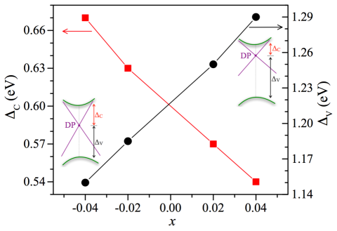
Fig. 5 illustrates change in the location of Dirac point due to the varying interlayer separation between graphene and MoS2 nanosheets. We observe that Dirac point shifts towards the MoS2 valence bands (i.e. increasing ) as we increase the compressive interlayer strain from +4% to -4%. This can be ascribed to the enhanced electric field effects arising due to the asymmetric interlayer potential. Such out-of-plane electric field or gate bias effects have also been demonstrated to open a gap at Dirac point in graphene. McCann (2006); Castro et al. (2007); Mak et al. (2009); Koshino (2010); Suarez et al. (2011); Munoz et al. (2016)
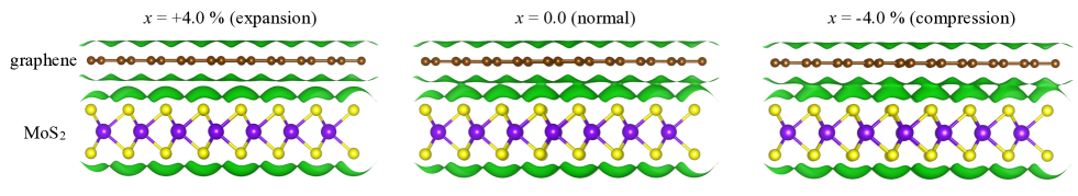
In order to appreciate any possible changes in the electronic density at the interface, charge isosurface has been plotted in Fig. 6. Differences from the isolated layers case can be detected for low values of electronic densities, in fact an overlap between the charge densities of both monolayers is found for =0.007 a.u. at ambient condition ( = 0), which increases with increasing interlayer compression, however, such charge density overlap is not present for the 4% expansion, as depicted in Fig. 6. Such charge accumulation between the graphene and MoS2 nanosheets aids to the opening of bandgap at Dirac point, as suggested by McCann. McCann (2006) Although uniaxial strains effects were found to cause notable changes in the electronic properties of graphene/MoS2 bilayers, no significant changes were observed in the Mo-S, S-S and C-C bond lengths due to the varying interlayer separation in the studied range.
Structure () () () () 5:4 heterostructure 3877 6626 12484 21801 4:3 heterostructure 4262 6582 12692 20319
III.3 Vibrational properties of graphene/MoS2 bilayer heterostructures
A thorough understanding of the vibrational properties of vdW heterostructures is not only important for fundamental physics, but it also renders great insights into the observed mechanical, thermal and electronic properties in vdW heterostructures. Several recent studies have primarily focused on the vibrational properties of grapheneYan et al. (2008); Wang et al. (2009); Lui and Heinz (2013), graphiteWirtz and Rubio (2004), transition metal dichalcogenides (TMDs) Ding et al. (2011); Zhao et al. (2013), and their stacked vdW heterostructuresLui et al. (2015); Le et al. (2016). The interlayer phonon modes that arise due to the weak vdW interactions are of special interest in vdW structures. Lui and Heinz (2013); Zhao et al. (2013); Lui et al. (2015); Le et al. (2016) Therefore, in this section we investigate the vibrational properties of graphene/MoS2 2D heterostructures with a special focus on the observed interlayer phonon modes in the studied systems.
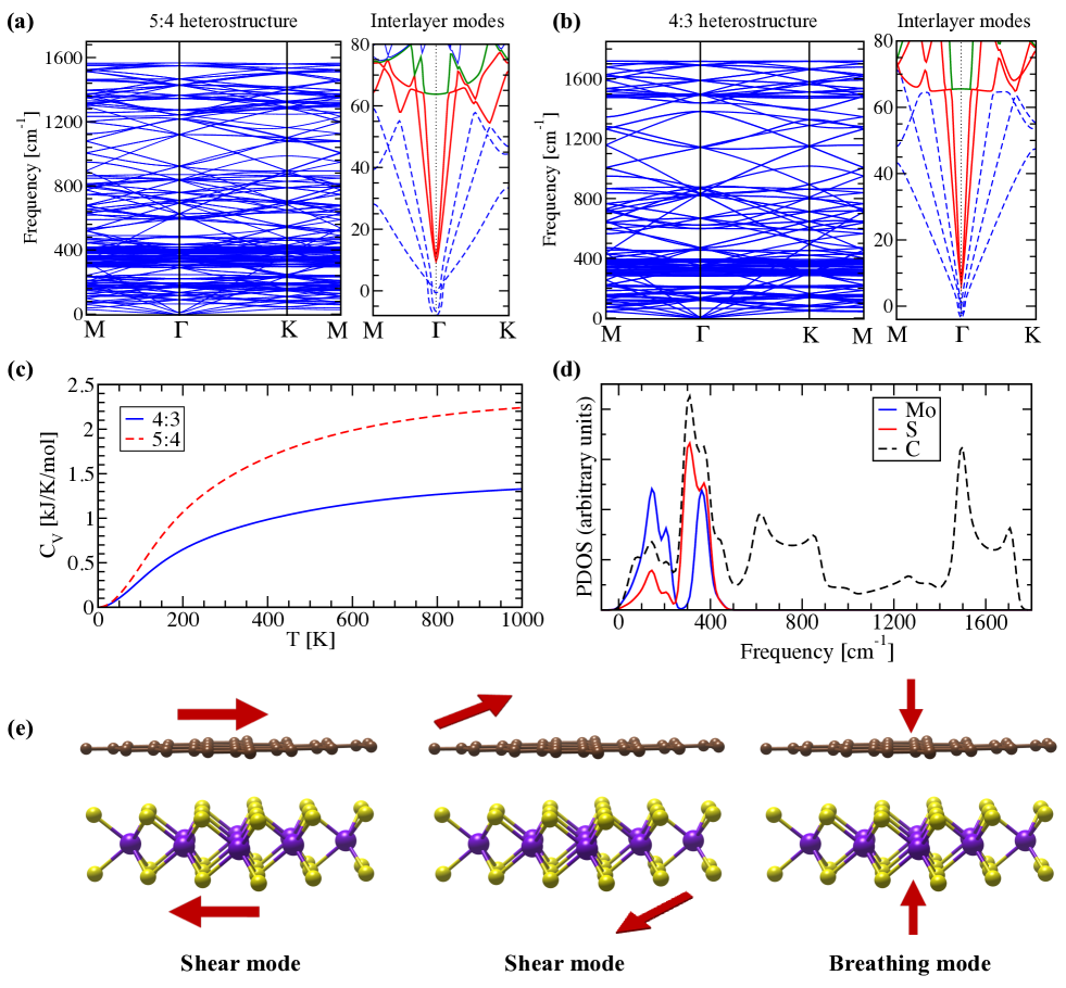
Figure 7 shows the phonon spectra, total and atom projected phonon density of states (PDOS) for 5:4 and 4:3 bilayer graphene/MoS2 structures, calculated using the DFPT approach as implemented in the VASP code. The SOC and vdW were included in the phonon calculations. We find that all the phonon modes have positive frequency (except for a very small imaginary frequency near which are often present in the theoretical calculations for 2D systems due to the inadequate numerical convergence close to =0 Singh and Romero (2017b)). The positive phonon frequencies guarantee the thermodynamical stability of the bilayer structures. The three lowest frequency phonon branches constitute , and acoustic modes. We also observe features of the flexural acoustic mode in the low frequency phonon dispersion very near the point. Flexural modes are particularly important for 2D systems and have been widely studied in 2D layered structures. Jiang et al. (2015) These modes significantly contribute to the PDOS and are responsible for the large thermal conductance. Le et al. Le et al. (2016) have reported that the transport due to the flexural excitations is almost ballistic.
Next to the three acoustic modes there exists the interlayer shear and breathing phonon modes. These vibrational modes describe the relative displacement of graphene sheet with respect to the MoS2 sheet in tangential (in-plane) and perpendicular (out-of-plane) directions. From the crystal symmetry, we expect two shear phonon modes and one breathing phonon mode as illustrated in Fig. 7(e). The breathing phonon mode is of particular importance since it is very sensitive to the interlayer vdW interaction and its count increases with increasing number of layers ) in a multilayer 2D vdW heterostructure. Depending upon , these low frequency modes can be Raman-active and/or IR-active.Zhao et al. (2013) In 5:4 (4:3) graphene/MoS2 bilayer, the frequency of the two shear modes and one breathing phonon mode at point is 9.53 (6.45), 11.75 (8.69) and 63.75 (65.54) cm-1, respectively. Note that the frequency of the breathing phonon mode is almost 10 times larger than that of the shear phonon modes. Moreover, the breathing phonon mode has almost zero dispersion in the phonon spectra near . These interlayer phonons modes play a vital role in understanding different underlying scattering mechanisms in layered 2D structures, and are very sensitive to the vDW interactions. The characteristic group velocity of the transverse acoustic (), longitudinal acoustic () and interlayer shear phonon modes is given Table 2. Our results are in good agreement with a recent work reported by Le al. Le et al. (2016) The atom resolved PDOS spectra reveals that all Mo, S and C atoms contribute to the acoustic modes, whereas, high frequency optical modes ( 500 ) have contribution only from the C atoms [see Fig. 7(d)]. Although the acoustic phonons mainly govern the heat transfer process, the optical phonons provide various scattering channels which could reduce the acoustic phonon life-times through acoustic-optic phonon scattering mechanisms.Pavlic et al. (2017) A very low lattice thermal conductivity is expected in graphene/MoS2 heterostructures along the vertical stacking direction due to the weak vdW bonding. The presence of multiple phonon band crossings in the phonon spectra (see Fig. 7) calls for a detailed investigation of the lattice thermal conductivity in graphene/MoS2 heterostructures.
The specific heat (CV) was determined from the phonons for both 5:4 and 4:3 bilayer heterostructures, and is shown in Fig. 7(c). Graphene/MoS2 bilayer heterostructures exhibit very large heat capacity compared to that of the constituent monolayers.Tohei et al. (2006); Yuan et al. (2015) Due to the large Debye temperature of graphene (1000 K)Tohei et al. (2006), the heat capacity of heterostructures approaches to its Dulong-Petit limit at high temperatures near 1000 K. Below 1000 K it follows the power law due to the dominant contribution from the lattice vibrations. The higher phonon density of states in 5:4 bilayer can be accounted for its larger heat capacity compared to that of in 4:3 bilayer. Due to their high heat capacity and outstanding cycling stability, graphene/MoS2 heterostructures are promising anode materials for batteries. Chang et al. (2011); Chang and Chen (2011); Shao et al. (2015); Fu et al. (2014)
IV Elastic Properties
The knowledge of elastic properties not only provides deep insights in understanding the nature of vdW interactions in graphene/MoS2 vdW heterostructures, but it is also essential for practical applications of such heterostructures in modern technology. Therefore, we have systematically evaluated the elastic stiffness constants () for 4:3 and 5:4 bilayer heterostructures using the stress-strain relationship as implemented in VASP code Kresse and Furthmüller (1996); Kresse and Joubert (1999), and further determined various elastic moduli using MechElastic script Singh and Romero (2017a); Singh et al. (2018b). The values of heterostructures are converged better than 2.0 N/m by increasing the -mesh size. Due to the hexagonal crystal geometry of system, only ), , and values are relevant. The 2D layer modulus, a quantity that represents the resistance of a nanosheet to stretching, can be calculated for hexagonal systems using equation:Andrew et al. (2012)
| (5) |
Shear modulus (= ) Layer modulus Young’s modulus Poisson’s ratio graphene/MoS2 bilayer (4:3) 500.0 109.7 194.0 304.2 395.0 0.22 This work graphene/MoS2 bilayer (5:4) 492.4 83.6 203.2 286.4 427.0 0.17 This work graphene/MoS2 bilayer - - - - 46748 - Ref.Liu et al. (2014) (Exp.) graphene 358.9 65.1 146.9 212.0 347.1 0.18 This work a 352.7 60.9 145.9 206.6 342.2 0.17 Ref.Andrew et al. (2012) (Theory) 358.1 60.4 148.9b 209.3b 348.0 0.17 Ref.Wei et al. (2009) (Theory) - - - - 34240 0.17 Ref.Lee et al. (2008) (Exp.) - - - - 34912 - Ref.Liu et al. (2014) (Exp.) MoS2 132.3 32.8 49.5 82.5 124.1 0.25 This worka 128.4 32.6 47.9b 80.5b 120.1 0.25b Ref.Peng and De (2013) (Theory) 130 40 45b 85b 117.7b 0.29 Ref.Cooper et al. (2013) (Theory) - - - - 123 0.25 Ref.Liu et al. (2014) (Exp.) a Elastic properties of isolated monolayer were calculated using VASP(PBE), and converged to less than 1.0 N/m by increasing -mesh size. b Estimated from the data reported in the reference.
Average 2D Young’s modulus (), Poisson’s ratio (), and shear modulus () can be obtained using following expressions:
| (6) |
Table 3 shows a list of the calculated elastic moduli for graphene/MoS2 bilayer heterostructures, isolated graphene and MoS2 monolayers. Our data are in excellent agreement with the reported values in literature from theoretical and experimental studies. We notice that although isolated graphene and MoS2 monolayer inherit complimentary physical properties, their combination mitigates the adverse elastic properties of each individual constituent providing a novel platform to engineer their properties. We notice that the values for graphene/MoS2 bilayers are roughly arithmetic sum of the values for isolated graphene and MoS2 monolayers. Overall elastic properties of bilayer heterostructure are better compared to that of the constituent monolayers. Notably, the elastic stiffness constants (except ) attain lower values ( elastic softening) in 5:4 bilayer compared to that of in 4:3 bilayer. The following two reasons are primarily responsible for the observed elastic softening: (i) The 5:4 bilayer inherits lower lattice mismatch than 4:3 bilayer, therefore it suffers lesser in-plane strain energy, and thereby reduces the effective elastic stiffness, and (ii) the nonlinear elastic response of the constituent monolayers.Lee et al. (2008); Cooper et al. (2013) The coefficient of the second-order term in the nonlinear elastic response is generally negative for most of the materials, which leads to a decrease (increase) in the elastic stiffness at large tensile (compressive) strains.Lee et al. (2008) In 5:4 bilayer, the graphene sheet undergoes a tensile strain of 1.2%, whereas graphene sheet undergoes a compressive strain of 1.4% in 4:3 bilayer heterostructure. On the other hand, the larger interlayer spacing and hence lesser vdW energy ( eV/atom) in 4:3 bilayer could be held accountable for lower shear elastic modulus compared to that of in 5:4 bilayer (vdW energy eV/atom).
We further study the intrinsic strength, bending modulus, and buckling phenomenon in graphene/MoS2 heterostructures. The intrinsic strength () can be estimated using the Griffith’s proposal: .Griffith (1921); Cooper et al. (2013) From values listed in Table 3, one can notice that the intrinsic strength of bilayer heterostructures is considerably larger than that of the isolated monolayers. The bending modulus () for a 2D nanosheet can be calculated using equation:Jiang (2015)
| (7) |
where, is the thickness of the nanosheet. Accurate determination of is uncertain because of the electronic configuration along the normal direction, which is subject to change under deformation. Due to this uncertinity, could acquire different values depending upon the chosen . However, the lower estimate of can be calculated using the absolute thickness of the nanosheet. For example: the absolute thickness of graphene is 0.6 – 0.8 ÅTu and Ou-Yang (2002), and for MoS2 is 3.13 Å (see Fig. 1). Considering the absolute thickness of graphene/MoS2 5:4 bilayer heterostructure ( = 3.13+3.40+0.75Tu and Ou-Yang (2002) = 7.28 Å), the obtained is 121.2 eV. The experimental value of for graphene/MoS2 heterostructures lies in range 10 – 11 Å.Yu et al. (2014); Zhang et al. (2014); Fu et al. (2014); Miwa et al. (2015) For = 10.5 Å, obtained = 252.2 eV. The reported values (lower estimates) for graphene and MoS2 monolayers are 1.2 eV and 9.61 eV.Jiang (2015) It is worth to note that although it is easier to bend an isolated graphene and MoS2 monolayer, their combination yields very large bending energy due to its multilayer atomic structure, which offers more interaction terms restraining the bending motion.
From the knowledge of quantities and , one can study the buckling phenomenon and estimate the critical buckling strain () using the Euler’s buckling theorem:Jiang (2015)
| (8) |
where, is the length of 2D nanosheet. For isolated graphene, MoS2 monolayer, and graphene/MoS2 5:4 bilayer heterostructure, we obtain following expressions:
| (9) |
Here, is in Å units. For the same length samples, the critical buckling strain for graphene/MoS2 5:4 bilayer heterostructure (MoS2 monolayer) is more than eighty (twenty) times larger compared to that of in graphene. Therefore, graphene/MoS2 bilayer heterostructures are more robust for in-plane structural deformations and do not buckle easily compared to the individual constituent layers. Hence, in this respect, graphene/MoS2 bilayer heterostructures are better fit for practical applications.
V Conclusions
In this study we report that compared to the available DFT vdW methods, the DFT-TS method best describes the weak vdW interactions and predicts the interlayer spacing accurately in graphene/MoS2 vdW heterostructures. The key reason behind the success of this method is the fact that the local variations of the charge-density near the interface are well captured in the TS-method. Therefore, the TS-method appears to be the best candidate to evaluate the weak vdW interactions at (semi)metallic/insulating interfaces. The predicted interlayer spacing for graphene/MoS2 bilayer structure (55 / 44) is 3.40 Å which is in excellent agreement with the experimental data. The electronic bandstructure analysis of 5:4 and 4:3 graphene/MoS2 bilayers reveals that the Dirac point of graphene is shifted upwards above the Fermi-level and is located near the conduction bands of MoS2 sheet, yielding a considerable charge-transfer process in 4:3 bilayer, whereas the Dirac point lies in the bandgap region in 5:4 bilayer indicating no charge-transfer process. We find that the location of Dirac point can be shifted by tuning the interlayer spacing between the graphene and MoS2 sheets. The vibrational spectra of 5:4 and 4:3 graphene/MoS2 bilayers reveals the presence of interlayer shear and breathing phonon modes in the bilayers. These interlayer phonons modes play a vital role in understanding different underlying scattering mechanisms in layered 2D structures. The graphene/MoS2 bilayer heterostructures possess large heat capacity, and exhibit much better elastic and mechanical properties compared to that of the isolated constituent monolayers. Elastic stiffness constants, elastic moduli, intrinsic strength, bending modulus, and buckling phenomenon for isolated graphene, MoS2 monolayer, and graphene/MoS2 bilayer heterostructures have been discussed along with a comparison with the available data in the literature.
Acknowledgments: This work used the Extreme Science and Engineering Discovery Environment (XSEDE), which is supported by National Science Foundation grant number OCI-1053575. Additionally, the authors acknowledge the support from Texas Advances Computer Center (TACC), Bridges supercomputer at Pittsburgh Supercomputer Center and Super Computing Systems (Spruce and Mountaineer) at West Virginia University (WVU). A.H.R. and S.S. acknowledge the support from National Science Foundation (NSF) DMREF-NSF 1434897 and DOE DE-SC0016176 projects. S.S. thanks the donors of Jefimenko family for their financial support through the Oleg D. and Valentina P. Jefimenko Physics Fellowship at WVU. S.S. also acknowledges the support from the Robert T. Bruhn research award and the WVU Foundation Distinguished Doctoral Fellowship. C.E. acknowledges support from Dirección de Investigación, Creaci n y Extensión at UTADEO. Authors thank Prof. Sergio E. Ulloa for fruitful discussions.
References
- Novoselov et al. (2004) K. S. Novoselov, A. K. Geim, S. V. Morozov, D. Jiang, Y. Zhang, S. V. Dubonos, I. V. Grigorieva, and A. A. Firsov, Science 306, 666 (2004).
- Novoselov et al. (2012) K. S. Novoselov, V. I. Falko, L. Colombo, P. R. Gellert, M. G. Schwab, and K. Kim, Nature 490, 192 (2012).
- Castro Neto et al. (2009) A. H. Castro Neto, F. Guinea, N. M. R. Peres, K. S. Novoselov, and A. K. Geim, Rev. Mod. Phys. 81, 109 (2009).
- Han et al. (2014) W. Han, R. K. Kawakami, M. Gmitra, and J. Fabian, Nature Nanotechnology 9, 794 EP (2014).
- Novoselov et al. (2016) K. S. Novoselov, A. Mishchenko, A. Carvalho, and A. H. Castro Neto, Science 353 (2016), 10.1126/science.aac9439.
- Singh et al. (2018a) S. Singh, A. M. Alsharari, S. E. Ulloa, and A. H. Romero, arXiv 1806.11469 (2018a).
- Qian et al. (2015) X. Qian, Y. Wang, W. Li, J. Lu, and J. Li, 2D Materials 2, 032003 (2015).
- RadisavljevicB. et al. (2011) RadisavljevicB., RadenovicA., BrivioJ., GiacomettiV., and KisA., Nat Nano 6, 147 (2011).
- Roy et al. (2013) K. Roy, M. Padmanabhan, S. Goswami, T. P. Sai, G. Ramalingam, S. Raghavan, and A. Ghosh, Nat Nano 8, 826 (2013).
- Bertolazzi et al. (2013) S. Bertolazzi, D. Krasnozhon, and A. Kis, ACS Nano 7, 3246 (2013).
- Sup Choi et al. (2013) M. Sup Choi, G.-H. Lee, Y.-J. Yu, D.-Y. Lee, S. Hwan Lee, P. Kim, J. Hone, and W. Jong Yoo, Nature communications 4, 1624 EP (2013).
- Britnell et al. (2013) L. Britnell, R. M. Ribeiro, A. Eckmann, R. Jalil, B. D. Belle, A. Mishchenko, Y.-J. Kim, R. V. Gorbachev, T. Georgiou, S. V. Morozov, A. N. Grigorenko, A. K. Geim, C. Casiraghi, A. H. C. Neto, and K. S. Novoselov, Science 340, 1311 (2013).
- Larentis et al. (2014) S. Larentis, J. R. Tolsma, B. Fallahazad, D. C. Dillen, K. Kim, A. H. MacDonald, and E. Tutuc, Nano Letters 14, 2039 (2014).
- Yu et al. (2014) L. Yu, Y.-H. Lee, X. Ling, E. J. G. Santos, Y. C. Shin, Y. Lin, M. Dubey, E. Kaxiras, J. Kong, H. Wang, and T. Palacios, Nano Letters 14, 3055 (2014).
- Chhowalla et al. (2013) M. Chhowalla, H. S. Shin, G. Eda, L.-J. Li, K. P. Loh, and H. Zhang, Nat Chem 5, 263 (2013).
- Lu et al. (2014) C.-P. Lu, G. Li, K. Watanabe, T. Taniguchi, and E. Y. Andrei, Phys. Rev. Lett. 113, 156804 (2014).
- Zhang et al. (2014) W. Zhang, C.-P. Chuu, J.-K. Huang, C.-H. Chen, M.-L. Tsai, Y.-H. Chang, C.-T. Liang, Y.-Z. Chen, Y.-L. Chueh, J.-H. He, M.-Y. Chou, and L.-J. Li, Scientific Reports 4, 3826 EP (2014).
- Deng et al. (2016) D. Deng, K. S. Novoselov, Q. Fu, N. Zheng, Z. Tian, and X. Bao, Nature Nanotechnology 11, 218 (2016), copyright - Copyright Nature Publishing Group Mar 2016; Last updated - 2016-03-03.
- Chang et al. (2011) K. Chang, W. Chen, L. Ma, H. Li, H. Li, F. Huang, Z. Xu, Q. Zhang, and J.-Y. Lee, J. Mater. Chem. 21, 6251 (2011).
- Chang and Chen (2011) K. Chang and W. Chen, Chem. Commun. 47, 4252 (2011).
- Shao et al. (2015) X. Shao, K. Wang, R. Pang, and X. Shi, The Journal of Physical Chemistry C 119, 25860 (2015).
- Šljivančanin and Belić (2017) Ž. Šljivančanin and M. Belić, Phys. Rev. Materials 1, 044003 (2017).
- Hohenberg and Kohn (1964) P. Hohenberg and W. Kohn, Phys. Rev. 136, B864 (1964).
- Kohn and Sham (1965) W. Kohn and L. J. Sham, Phys. Rev. 140, A1133 (1965).
- Grimme (2006) S. Grimme, Journal of Computational Chemistry 27, 1787 (2006).
- Gmitra and Fabian (2015) M. Gmitra and J. Fabian, Phys. Rev. B 92, 155403 (2015).
- Ebnonnasir et al. (2014) A. Ebnonnasir, B. Narayanan, S. Kodambaka, and C. V. Ciobanu, Applied Physics Letters 105, 031603 (2014).
- Klimeš et al. (2011) J. c. v. Klimeš, D. R. Bowler, and A. Michaelides, Phys. Rev. B 83, 195131 (2011).
- Li et al. (2013a) X. D. Li, S. Yu, S. Q. Wu, Y. H. Wen, S. Zhou, and Z. Z. Zhu, The Journal of Physical Chemistry C 117, 15347 (2013a).
- Ma et al. (2011) Y. Ma, Y. Dai, M. Guo, C. Niu, and B. Huang, Nanoscale 3, 3883 (2011).
- Le et al. (2016) N. B. Le, T. D. Huan, and L. M. Woods, ACS Applied Materials & Interfaces 8, 6286 (2016).
- Hu et al. (2016) W. Hu, T. Wang, R. Zhang, and J. Yang, Journal of Materials Chemistry C 4, 1776 (2016).
- Nguyen (2018) C. V. Nguyen, Superlattices and Microstructures 116, 79 (2018).
- Pierucci et al. (2016) D. Pierucci, H. Henck, J. Avila, A. Balan, C. H. Naylor, G. Patriarche, Y. J. Dappe, M. G. Silly, F. Sirotti, A. T. C. Johnson, M. C. Asensio, and A. Ouerghi, Nano Letters 16, 4054 (2016).
- Yan et al. (2008) J.-A. Yan, W. Y. Ruan, and M. Y. Chou, Phys. Rev. B 77, 125401 (2008).
- Sofo et al. (2007) J. O. Sofo, A. S. Chaudhari, and G. D. Barber, Phys. Rev. B 75, 153401 (2007).
- Wang et al. (2009) H. Wang, Y. Wang, X. Cao, M. Feng, and G. Lan, Journal of Raman Spectroscopy 40, 1791 (2009).
- Lui and Heinz (2013) C. H. Lui and T. F. Heinz, Phys. Rev. B 87, 121404 (2013).
- Ding et al. (2011) Y. Ding, Y. Wang, J. Ni, L. Shi, S. Shi, and W. Tang, Physica B: Condensed Matter 406, 2254 (2011).
- Zhao et al. (2013) Y. Zhao, X. Luo, H. Li, J. Zhang, P. T. Araujo, C. K. Gan, J. Wu, H. Zhang, S. Y. Quek, M. S. Dresselhaus, and Q. Xiong, Nano Letters 13, 1007 (2013).
- Jiang et al. (2015) J.-W. Jiang, B.-S. Wang, J.-S. Wang, and H. S. Park, Journal of Physics: Condensed Matter 27, 083001 (2015).
- Tohei et al. (2006) T. Tohei, A. Kuwabara, F. Oba, and I. Tanaka, Phys. Rev. B 73, 064304 (2006).
- Yuan et al. (2015) J. Yuan, Z. Lv, Q. Lu, Y. Cheng, X. Chen, and L. Cai, Solid State Sciences 40, 1 (2015).
- Lee et al. (2008) C. Lee, X. Wei, J. W. Kysar, and J. Hone, Science 321, 385 (2008).
- Cooper et al. (2013) R. C. Cooper, C. Lee, C. A. Marianetti, X. Wei, J. Hone, and J. W. Kysar, Phys. Rev. B 87, 035423 (2013).
- Jiang (2015) J.-W. Jiang, Frontiers of Physics 10, 287 (2015).
- Andrew et al. (2012) R. C. Andrew, R. E. Mapasha, A. M. Ukpong, and N. Chetty, Phys. Rev. B 85, 125428 (2012).
- Wei et al. (2009) X. Wei, B. Fragneaud, C. A. Marianetti, and J. W. Kysar, Phys. Rev. B 80, 205407 (2009).
- Liu et al. (2014) K. Liu, Q. Yan, M. Chen, W. Fan, Y. Sun, J. Suh, D. Fu, S. Lee, J. Zhou, S. Tongay, J. Ji, J. B. Neaton, and J. Wu, Nano Letters 14, 5097 (2014).
- Peng and De (2013) Q. Peng and S. De, Phys. Chem. Chem. Phys. 15, 19427 (2013).
- Tkatchenko and Scheffler (2009) A. Tkatchenko and M. Scheffler, Phys. Rev. Lett. 102, 073005 (2009).
- Kresse and Furthmüller (1996) G. Kresse and J. Furthmüller, Phys. Rev. B 54, 11169 (1996).
- Kresse and Joubert (1999) G. Kresse and D. Joubert, Phys. Rev. B 59, 1758 (1999).
- Perdew et al. (1996) J. P. Perdew, K. Burke, and M. Ernzerhof, Phys. Rev. Lett. 77, 3865 (1996).
- Bučko et al. (2013) T. c. v. Bučko, S. Lebègue, J. Hafner, and J. G. Ángyán, Phys. Rev. B 87, 064110 (2013).
- Togo et al. (2008) A. Togo, F. Oba, and I. Tanaka, Phys. Rev. B 78, 134106 (2008).
- Romero and Munoz (2015) A. H. Romero and F. Munoz, “Pyprocar code,” (2015).
- Singh et al. (2016a) S. Singh, A. C. Garcia-Castro, I. Valencia-Jaime, F. Muñoz, and A. H. Romero, Phys. Rev. B 94, 161116 (2016a).
- Singh et al. (2016b) S. Singh, W. Ibarra-Hernandez, I. Valencia-Jaime, G. Avendano-Franco, and A. H. Romero, Phys. Chem. Chem. Phys. 18, 29771 (2016b).
- Singh and Romero (2017a) S. Singh and A. H. Romero, “MechElastic code,” (2017a).
- Gonze et al. (2016) X. Gonze, F. Jollet, F. A. Araujo, D. Adams, B. Amadon, T. Applencourt, C. Audouze, J.-M. Beuken, J. Bieder, A. Bokhanchuk, E. Bousquet, F. Bruneval, D. Caliste, M. Côté, F. Dahm, F. D. Pieve, M. Delaveau, M. D. Gennaro, B. Dorado, C. Espejo, G. Geneste, L. Genovese, A. Gerossier, M. Giantomassi, Y. Gillet, D. Hamann, L. He, G. Jomard, J. L. Janssen, S. L. Roux, A. Levitt, A. Lherbier, F. Liu, I. Lukačević, A. Martin, C. Martins, M. Oliveira, S. Poncé, Y. Pouillon, T. Rangel, G.-M. Rignanese, A. Romero, B. Rousseau, O. Rubel, A. Shukri, M. Stankovski, M. Torrent, M. V. Setten, B. V. Troeye, M. Verstraete, D. Waroquiers, J. Wiktor, B. Xu, A. Zhou, and J. Zwanziger, Computer Physics Communications 205, 106 (2016).
- Grimme et al. (2010) S. Grimme, J. Antony, S. Ehrlich, and H. Krieg, The Journal of Chemical Physics 132, 154104 (2010).
- Van Troeye et al. (2016) B. Van Troeye, M. Torrent, and X. Gonze, Phys. Rev. B 93, 144304 (2016).
- Hamann (2013) D. R. Hamann, Phys. Rev. B 88, 085117 (2013).
- van Setten et al. (2017) M. J. van Setten, M. Giantomassi, E. Bousquet, M. J. Verstraete, D. R. Hamann, X. Gonze, and G.-M. Rignanese, arXiv 1710.10138 (2017).
- Lebedeva et al. (2017) I. V. Lebedeva, A. V. Lebedev, A. M. Popov, and A. A. Knizhnik, Computational Materials Science 128, 45 (2017).
- Hirshfeld (1971) F. L. Hirshfeld, Acta Crystallographica Section B 27, 769 (1971).
- Ramasubramaniam (2012) A. Ramasubramaniam, Phys. Rev. B 86, 115409 (2012).
- Espejo et al. (2013) C. Espejo, T. Rangel, A. H. Romero, X. Gonze, and G.-M. Rignanese, Phys. Rev. B 87, 245114 (2013).
- Amin et al. (2015) B. Amin, N. Singh, and U. Schwingenschlögl, Phys. Rev. B 92, 075439 (2015).
- Ouma et al. (2017) C. N. M. Ouma, S. Singh, K. O. Obodo, G. O. Amolo, and A. H. Romero, Phys. Chem. Chem. Phys. , (2017).
- Gmitra et al. (2009) M. Gmitra, S. Konschuh, C. Ertler, C. Ambrosch-Draxl, and J. Fabian, Phys. Rev. B 80, 235431 (2009).
- Konschuh et al. (2010) S. Konschuh, M. Gmitra, and J. Fabian, Phys. Rev. B 82, 245412 (2010).
- Gmitra et al. (2017) M. Gmitra, D. Kochan, P. Högl, and J. Fabian, Spin Orbitronics And Topological Properties Of Nanostructures-Lecture Notes Of The Twelfth International School On Theoretical Physics , 18 (2017).
- Alsharari et al. (2016) A. M. Alsharari, M. M. Asmar, and S. E. Ulloa, Phys. Rev. B 94, 241106 (2016).
- Gmitra et al. (2016) M. Gmitra, D. Kochan, P. Högl, and J. Fabian, Phys. Rev. B 93, 155104 (2016).
- Gmitra and Fabian (2017) M. Gmitra and J. Fabian, Phys. Rev. Lett. 119, 146401 (2017).
- Splendiani et al. (2010) A. Splendiani, L. Sun, Y. Zhang, T. Li, J. Kim, C.-Y. Chim, G. Galli, and F. Wang, Nano Letters 10, 1271 (2010).
- Naik and Jain (2017) M. H. Naik and M. Jain, Phys. Rev. B 95, 165125 (2017).
- Su et al. (2017) X. Su, H. Cui, W. Ju, Y. Yong, and X. Li, Modern Physics Letters B 31, 1750229 (2017).
- Li et al. (2013b) X. D. Li, S. Yu, S. Q. Wu, Y. H. Wen, S. Zhou, and Z. Z. Zhu, The Journal of Physical Chemistry C 117, 15347 (2013b).
- Coy Diaz et al. (2015) H. Coy Diaz, J. Avila, C. Chen, R. Addou, M. C. Asensio, and M. Batzill, Nano Letters 15, 1135 (2015).
- Wang et al. (2015) Z. Wang, Q. Chen, and J. Wang, The Journal of Physical Chemistry C 119, 4752 (2015).
- Oakes et al. (2016) L. Oakes, R. Carter, T. Hanken, A. P. Cohn, K. Share, B. Schmidt, and C. L. Pint, Nature communications 7 (2016), 10.1038/ncomms11796.
- Pandey et al. (2016) T. Pandey, A. P. Nayak, J. Liu, S. T. Moran, J.-S. Kim, L.-J. Li, J.-F. Lin, D. Akinwande, and A. K. Singh, Small 12, 4063 (2016).
- Liu et al. (2016) X. Liu, I. Balla, H. Bergeron, G. P. Campbell, M. J. Bedzyk, and M. C. Hersam, ACS Nano 10, 1067 (2016).
- Liu and Li (2015) X. Liu and Z. Li, The Journal of Physical Chemistry Letters 6, 3269 (2015).
- Xu et al. (2017) L. Xu, W.-Q. Huang, W. Hu, K. Yang, B.-X. Zhou, A. Pan, and G.-F. Huang, Chemistry of Materials 29, 5504 (2017).
- McCann (2006) E. McCann, Phys. Rev. B 74, 161403 (2006).
- Castro et al. (2007) E. V. Castro, K. S. Novoselov, S. V. Morozov, N. M. R. Peres, J. M. B. L. dos Santos, J. Nilsson, F. Guinea, A. K. Geim, and A. H. C. Neto, Phys. Rev. Lett. 99, 216802 (2007).
- Mak et al. (2009) K. F. Mak, C. H. Lui, J. Shan, and T. F. Heinz, Phys. Rev. Lett. 102, 256405 (2009).
- Koshino (2010) M. Koshino, Phys. Rev. B 81, 125304 (2010).
- Suarez et al. (2011) A. M. Suarez, L. R. Radovic, E. Bar-Ziv, and J. O. Sofo, Phys. Rev. Lett. 106, 146802 (2011).
- Munoz et al. (2016) F. Munoz, H. P. O. Collado, G. Usaj, J. O. Sofo, and C. A. Balseiro, Phys. Rev. B 93, 235443 (2016).
- Wirtz and Rubio (2004) L. Wirtz and A. Rubio, Solid State Communications 131, 141 (2004).
- Lui et al. (2015) C. H. Lui, Z. Ye, C. Ji, K.-C. Chiu, C.-T. Chou, T. I. Andersen, C. Means-Shively, H. Anderson, J.-M. Wu, T. Kidd, Y.-H. Lee, and R. He, Phys. Rev. B 91, 165403 (2015).
- Singh and Romero (2017b) S. Singh and A. H. Romero, Phys. Rev. B 95, 165444 (2017b).
- Pavlic et al. (2017) O. Pavlic, W. Ibarra-Hernandez, I. Valencia-Jaime, S. Singh, G. Avendaño-Franco, D. Raabe, and A. H. Romero, Journal of Alloys and Compounds 691, 15 (2017).
- Fu et al. (2014) W. Fu, F.-H. Du, J. Su, X.-H. Li, X. Wei, T.-N. Ye, K.-X. Wang, and J.-S. Chen, Scientific reports 4 (2014), 10.1038/srep04673.
- Singh et al. (2018b) S. Singh, I. Valencia-Jaime, O. Pavlic, and A. H. Romero, Phys. Rev. B 97, 054108 (2018b).
- Griffith (1921) A. A. Griffith, Philosophical Transactions of the Royal Society of London A: Mathematical, Physical and Engineering Sciences 221, 163 (1921).
- Tu and Ou-Yang (2002) Z.-c. Tu and Z.-c. Ou-Yang, Phys. Rev. B 65, 233407 (2002).
- Miwa et al. (2015) J. A. Miwa, M. Dendzik, S. S. Grønborg, M. Bianchi, J. V. Lauritsen, P. Hofmann, and S. Ulstrup, ACS Nano 9, 6502 (2015).