Energy-Efficient CMOS Memristive Synapses for Mixed-Signal Neuromorphic System-on-a-Chip
Abstract
Emerging non-volatile memory (NVM), or memristive, devices promise energy-efficient realization of deep learning, when efficiently integrated with mixed-signal integrated circuits on a CMOS substrate. Even though several algorithmic challenges need to be addressed to turn the vision of memristive Neuromorphic Systems-on-a-Chip (NeuSoCs) into reality, issues at the device and circuit interface need immediate attention from the community. In this work, we perform energy-estimation of a NeuSoC system and predict the desirable circuit and device parameters for energy-efficiency optimization. Also, CMOS synapse circuits based on the concept of CMOS memristor emulator are presented as a system prototyping methodology, while practical memristor devices are being developed and integrated with general-purpose CMOS. The proposed mixed-signal memristive synapse can be designed and fabricated using standard CMOS technologies and open doors to interesting applications in cognitive computing circuits.
Index Terms:
CMOS Neurons, Memristors, Neuromorphic computing, Spiking Neural Networks (SNNs), STDP, Synapses.I Introduction
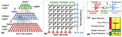
A grand challenge for the semiconductor industry is to “Create a new type of computer that can proactively interpret and learn from data, solve unfamiliar problems using what it has learned, and operate with the energy-efficiency of the human brain [1].” Deep neural networks, or deep learning, have been remarkably successful with a growing repertoire of problems in image and video interpretation, speech recognition, control, and natural language processing [2]. However, these implementations are compute intensive and employ high-end servers with graphical processing units (GPUs) to train deep neural networks. Furthermore, the new International Roadmap for Devices and Systems (IRDS) that replaces the ITRS roadmap, looks forward to More-Moore and Beyond-Moore technologies to develop radically different data-centric computing architectures [3, 4]. New architectures are required to transcend the device variability and interconnect scaling bottlenecks in nano-scale CMOS, should exploit massive parallelism, and employ in-memory computing as inspired from biological brains. Recent progress in memristive or resistance-switching devices (RRAM, STTRAM, phase-change memory, etc.) has spurred renewed interest in neuromorphic computing [5, 6, 7, 8, 9, 10, 11]. Such memristive devices, integrated with standard CMOS technology, are expected to realize low-power neuromorphic system-on-a-chip (NeuSoC) with embedded deep learning and orders of magnitude lower power consumption than GPUs, as illustrated in Fig. 1 [12, 13]. Since ‘analog’ memristor device technology is yet to mature while practical demonstration in neural circuits are being pursued [14, 15, 16], we earlier proposed a low-risk and robust alternative for circuit prototyping using a CMOS memristor emulator [17, 18]. In this work, we extend this CMOS memristor concept to memristive synapse circuits that realize bio-plausible spike-timing dependent plasticity (STDP) learning. The rest of the manuscript is organized as follows: Section II presents energy-estimation of memristive NeuSoCs; Section III and IV describe the CMOS memristor and synapse circuits. Finally Section V presents simulation results and application in an image classification task, followed by conclusion.
II Energy-efficiency of Neuromorphic SoCs
The primary motivation of exploring memristive (or emerging NVM-based) spiking neural network is to achieve orders of magnitude energy-efficiency improvement over the contemporary digital architectures. This is expected to be achieved by employing event-driven asynchronous spiking neural networks (SNNs), with low-power circuits and ultra-low-power synaptic (memory) devices. In an SNN, the spike shape parameters and the low-resistance state (LRS) resistance, , of the memristive devices ( is typically order(s) of magnitude higher than ) contribute to the energy consumed in an spike event. The total energy consumption is also decided by the sparsity, i.e. the percentage of synapses in LRS state, spiking activity, and the power consumption in the CMOS neurons. Assuming a rectangular spike pulse-shape of amplitude and width , the current input signal is , and the energy consumption for a spike driving a synapse with resistance , , is given by .
The approximate SNN energy consumption for one event can be formulated as
| (1) |
where is the sparsity factor (i.e. the fraction of neurons firing on average), is fraction of synapses in the LRS-state, is the number of synaptic connections, is the number of neurons. is the neuron power consumption; energy consumed in the peripheral circuits is ignored to simplify the analysis. To provide a rough system-level comparison, the AlexNet convolutional neural network for deep learning used for the Imagenet Challenge comprised of 61M synaptic weights and 640k neurons [19]. We assume that an equivalent SNN is constructed through transfer learning [20], or spike-based equivalent of backpropagation algorithm [21]; the circuit architecture is essentially the same. With an estimation based on the RRAM-compatible spiking neuron chip realized in [22], 4-bit compound memristive synapses[23, 14, 15], and ranging from 0.1-10, the energy consumption for processing (training or classification) of one image is shown in Table I. By comparing with the contemporary advanced GPU Nvidia P4 [24] (170 images/s/W), a memristive architecture with provides a meagre improvement in energy-efficiency. However, the energy consumption can be significantly reduced if the LRS resistance of the memristive devices can be increased to high- regime, leading to a potential range performance improvement; high LRS also helps reduce the power consumption in the opamp-based neuron circuits [22, 25].Since there has been less focus on realizing high-LRS devices as the multi-valued memristive devices are still under development, circuit solutions are desired to address this wide energy-efficiency gap.
| Low | Medium | High | ||
| Spike Width | 100ns | |||
| Spike Amplitude | 300mV | |||
| ON State Resistance | ||||
| Single Spike Energy | 1.4pJ | 140fJ | 14fJ | |
| Neuron Energy | 1.56pJ | 260fJ | 43.3fJ | |
| Neuron Sparsity | 0.6 | |||
| On State RRAM Ratio | 0.5 | |||
| Single Event Energy | ||||
| Images / Sec / Watt | 2.4k | 23.6k | 235k | |
| Acceleration over GPU[24] | ||||
III CMOS Memristor
Memristor was defined as a two-terminal circuit-theoretic concept in [26], and later extended to a wider class of memristive devices [27]. The fundamental promise of the memristive devices lies in their ‘analog’ memory, that enables them to store as well as manipulate information in analog-domain. This is harnessed in neuromorphic computing, where memristors realize incremental synapses that learn based on STDP, a bio-inspired local learning rule that implements spike-based expectation maximization (SEM) algorithm [12, 28, 29, 30, 15, 21]. The author recently proposed a compact CMOS memristor (emulator) circuit [17, 18]. The fundamental concept is illustrated in Fig. 2 (a&b), where an n-channel MOSFET (NMOS) implements a floating variable resistance between terminals A and B. The transconductor senses the voltage across the two terminals, produces a small-signal current which is integrated as charge on capacitor . When the strobe is low, the capacitor is disconnected from the transconductor and holds the stored charge; thus realizing a dynamic analog memory.
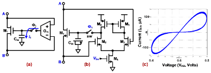
Here, the voltage on the capacitor, , controls the gate of and is thus the ‘state,’ , of the synapse. The switch () prevents ’s output from leaking the state ) on capacitor when no inputs are applied. Assuming that is in triode, the dynamics of the memristor circuit are approximated as
| (2) |
| (3) |
where and are the gate-to-source and threshold voltages; , is the transconductance parameter, is the sizing for . In order to force in triode for large drain-source voltage swings, a zero- or low-threshold voltage (ZVT/LVT) transistor is employed [17, 18]. The simulated current-voltage characteristics for the memristor circuit, seen in Fig. 2 (c), confirms the pinched hysteresis signature of an ideal memristor.
Contemporary memristive devices exhibit several limitations; they exhibit stochastic switching and variability in resistance states, depending upon the initial ‘forming’ step [31, 32, 33]. Further, it is challenging to realize stable multi-valued weights with filamentary devices [34, 15]; Oxide-switching devices have exhibited ~9 states and their performance in-situ a circuit is being investigated [35]. A greater impediment for realizing NeuSoCs is the lower LRS resistance observed in memristive devices ()[35], which leads to energy inefficiency as detailed earlier in Section II. Thus, it is desirable to realize CMOS based memristive synapses for enabling system-level exploration while the memristive devices mature in research.
IV Memristive Synapse Circuit
Memristive spiking circuits typically use analog spikes with rectangular positive pulse with a negative exponential tail [22]; however, representation of spikes with digital pulses is highly desirable for large-scale NeuSoC implementation. Further, an accelerated neural dynamics with moderate speed (few MHz’s) is preferred over biological time-scales (sub-kHz) for optimizing CMOS circuit area and energy consumption [36]. Current-output type bio-mimetic synapses are pervasive in literature ([37] and references therein), where subthreshold analog techniques were used to mimic synaptic ion-channel dynamics. Most recently, [38] reported a pair-wise STDP synapse with short-term retention, and [39] combined subthreshold circuits with a latch. In contrast, we have proposed memristive STDP-learning synapse concept shown in Figure 3 and was previously disclosed by us in [17]. In this work, we expand on the previous disclosure, and present circuits and system-level details. The circuit employs the trace decay method for emulating STDP as used in the event-driven simulators for computational neuroscience [40, 38, 39]. The STDP weight update block converts the relative timing between pre and post spikes () into change in , and thus the synaptic weight. Figure 3 (b) shows schematics for the synapse, and one of several possible transistor-level implementations is shown in Fig. 4. Here, the input pre and post pulses are converted into voltage traces and respectively, using the two Exponential Decay Circuit (EDC) blocks. The outputs of the EDCs are translated to a current using the shared , which are then integrated on . The exponential trace is implemented using active resistors, , with time-constants which can be independently tuned.
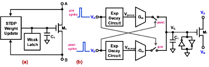
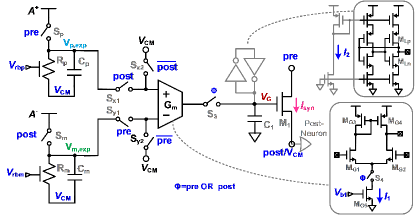
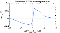
Figure 5 (a) illustrates the synapse operation and the resulting pair-wise additive STDP learning function is shown in Figure 5 (b). Here, the (pre)-synaptic spike arrives earlier than the (post)-synaptic spike. EDC output, , is then sampled by the post spike. This sampled voltage leads to an increase in the voltage (i.e. the state of the synapse) and increase in synaptic weight/conductance (); synapse undergoes short-term potentiation. Similarly, in the second case, the post spike arrives earlier than pre which in turn reduces the synapse state ; the synapse undergoes short-term depression. The references and determine the maximum synaptic potentiation/depression as .
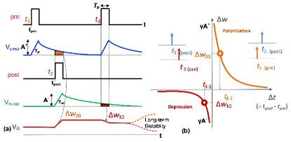
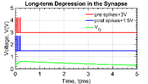
Even though the dynamic STDP synapses provide analog states, they can only realize short-term potentiation/depression as the capacitor memory leaks away in few milli-seconds. However in a NeuSoC, the final weights after training must be persistent and amenable for read-out/in. This is realized by employing long-term bistability in synapses where after short-term STDP learning, the weights are quantized to either a high or low binary conductance state. As shown in Figs. 3&4, a weak latch is connected to . This slow resolving subthreshold latch is designed for very large regeneration time-constants (1-5ms) such that it doesn’t interfere with the short-term STDP learning. However, once the STDP pulses are no longer present, the weak bistable latch slowly steers the state of the synapse to either a large voltage (LRS) or to a low-voltage (HRS) long-term states, which can easily be read-out.
| Device | Type | W/L, | Parameter | Value |
| NMOS | 500fF | |||
| PMOS | 100fF | |||
| NMOS | 10nA | |||
| PMOS | ~100pA | |||
| PMOS | ~90pA | |||
| NMOS | ~110pA | |||
| NMOS | ||||
| LVT NMOS | LRS | |||
| HRS |
The synapse circuit in Fig. 4 is implemented in a 130nm CMOS technology with supply . The transistor sizing and parameter values used in this circuit are listed in Table II. The memristive synapse, for the given sizing for , realizes LRS and HRS resistances of and respectively, providing significant improvement over contemporary memristive devices. As detailed in [22, 30], the traditional subthreshold neuron designs are not suitable for driving memristive load. The opamp-based integrate-and-fire neurons with winner-take-all STDP learning interface from author’s prior work in [30] can directly be adapted to interface with the presented synapses; higher LRS resistance will further help simply opamp design.
V Simulation Results
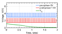
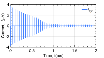
In this design, the total standby current drawn from is , while 10.4nA is drawn during the pre/post spike event. This results in a static power consumption of 588pW and dynamic energy consumption of 91.24fJ/spike (for ) in the LRS state. This circuit can be easily modified to different specifications and further optimized for energy-efficiency, area and speed. Figure 6 shows transient simulation for a single synapse; pre and post pulses are applied with , spaced by and the state voltage and synaptic current between pre and post terminals are displayed. We can observe that the weight undergoes monotonic decrease due to pair-wise STDP updates with a corresponding decrease in synapse weight/conductance, , and thus the synaptic current, .
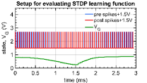
Next, a transient simulation shown in Fig. 7 is constructed to determine the STDP learning function for the synapse circuit. Here, pre and post spikes are applied with progressively changing from to with spacing of to allow the transients to completely decay. This results in approximate double-exponential learning function characteristic of pair-wise STDP function seen in Fig. 5(b).
Long-term bistability is demonstrated through simulations in Fig. 8 where spikes are applied such that the weight crosses the latch’s threshold point, in Fig. 8(left) and is below threshold in Fig. 8 (right). The weak latch is biased in subthreshold and has a regenerative time-constant of ; the latch slowly resolves the synaptic state to logic high (LRS) or low (LRS).

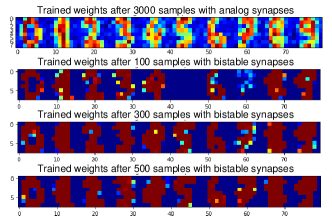
An SNN, similar to [30], was setup using the bistable memristive synapse and winner-take-all neuron macro-models using Brian2 libraries in Python [40]. The UCI handwritten digits dataset (3,823 training and 1,797 test bitmap images [41]) was used to train the fully-connected SNN with 64 input and 10 output neurons, 640 synapses, and with a teacher signal enforcing the output labels. Fig. 9 shows the learned weights for each output neuron. For analog synapses the test accuracy was 83% for all 10 digits (96% for 4 digits); the bistable synapses achieve accuracy of ~74% for 10 digits due to binary quantization during training. Care must be taken to ensure that is much larger than the time for which input samples are presented () to avoid catastrophic forgetting. In this experiment, the bistable SNN was trained for 500 images as a large number of weights, , start approaching , resulting in loss of classification accuracy. Further, must be used as otherwise there is a chance of all the weights getting quantized to 0, and the neurons will never fire.
VI Conclusion
A compact analog memristive STDP synapse circuit, with long-term binary retention and high LRS resistance, is introduced and designed in standard CMOS and analytical as well as simulation results are presented. The circuit is used to realize image classification application and the challenges are discussed. In summary, the synapse provides an efficient circuit solution for NeuSoC architecture exploration, while memristive devices on CMOS platforms reach maturity.
References
- [1] “A Nanotechnology-Inspired Grand Challenge for Future Computing,” October 2015. [Online]. Available: https://www.nano.gov/grandchallenges
- [2] G. E. Hinton and R. R. Salakhutdinov, “Reducing the dimensionality of data with neural networks,” Science, vol. 313, no. 5786, pp. 504–507, 2006.
- [3] “ International Roadmap for Devices and Systems (IRDS).” [Online]. Available: https://irds.ieee.org/reports
- [4] R. Courtland, “Transistors could stop shrinking in 2021,” IEEE Spectrum, vol. 53, no. 9, pp. 9–11, 2016.
- [5] D. B. Strukov, G. S. Snider, D. R. Stewart, and R. S. Williams, “The missing memristor found,” Nature, vol. 453, no. 7191, pp. 80–83, 2008.
- [6] A. Rothenbuhler, T. Tran, E. H. Barney Smith, V. Saxena, and K. A. Campbell, “Reconfigurable threshold logic gates using memristive devices,” Journal of Low Power Electronics and Applications, vol. 3, no. 2, pp. 174–193, 2013.
- [7] I. Vourkas and G. C. Sirakoulis, Memristor-based nanoelectronic computing circuits and architectures. Springer, 2016.
- [8] D. Kuzum, R. G. Jeyasingh, B. Lee, and H.-S. P. Wong, “Nanoelectronic programmable synapses based on phase change materials for brain-inspired computing,” Nano letters, vol. 12, no. 5, pp. 2179–2186, 2011.
- [9] S. H. Jo, K.-H. Kim, and W. Lu, “High-density crossbar arrays based on a si memristive system,” Nano letters, vol. 9, no. 2, pp. 870–874, 2009.
- [10] S. Gupta, V. Saxena, K. A. Campbell, and R. J. Baker, “W-2w current steering dac for programming phase change memory,” in Microelectronics and Electron Devices, 2009. WMED 2009. IEEE Workshop on. IEEE, 2009, pp. 1–4.
- [11] G. W. Burr, R. M. Shelby, A. Sebastian, S. Kim, S. Kim, S. Sidler, K. Virwani, M. Ishii, P. Narayanan, A. Fumarola et al., “Neuromorphic computing using non-volatile memory,” Advances in Physics: X, vol. 2, no. 1, pp. 89–124, 2017.
- [12] G. Indiveri, R. Legenstein, G. Deligeorgis, and T. Prodromakis, “Integration of nanoscale memristor synapses in neuromorphic computing architectures,” Nanotechnology, vol. 24, no. 38, p. 384010, 2013.
- [13] D. B. Strukov and K. K. Likharev, “A reconfigurable architecture for hybrid cmos/nanodevice circuits,” in Proceedings of the 2006 ACM/SIGDA 14th international symposium on Field programmable gate arrays. ACM, 2006, pp. 131–140.
- [14] X. Wu and V. Saxena, “Enabling Bio-Plausible Multi-level STDP using CMOS Neurons with Dendrites and Bistable RRAMs,” in International Joint Conference on Neural Networks (IJCNN), Alaska, USA, May 2017.
- [15] V. Saxena, X. Wu, I. Srivastava, and K. Zhu, “Towards spiking neuromorphic system-on-a-chip with bio-plausible synapses using emerging devices,” in Proceedings of the 4th ACM International Conference on Nanoscale Computing and Communication. ACM, 2017, p. 18.
- [16] C. D. Schuman, T. E. Potok, R. M. Patton, J. D. Birdwell, M. E. Dean, G. S. Rose, and J. S. Plank, “A survey of neuromorphic computing and neural networks in hardware,” arXiv preprint arXiv:1705.06963, 2017.
- [17] V. Saxena, “Memory controlled circuit system and apparatus,” Oct. 2015, US Patent App. 14/538,600. [Online]. Available: https://www.google.com/patents/US20150278682
- [18] ——, “A Compact CMOS Memristor Emulator Circuit and its Applications,” Arxiv prepint arXiv:1711.06819, 2017. [Online]. Available: https://arxiv.org/submit/2047040
- [19] A. Krizhevsky, I. Sutskever, and G. E. Hinton, “Imagenet classification with deep convolutional neural networks,” in Advances in neural information processing systems, 2012, pp. 1097–1105.
- [20] P. U. Diehl, D. Neil, J. Binas, M. Cook, S.-C. Liu, and M. Pfeiffer, “Fast-classifying, high-accuracy spiking deep networks through weight and threshold balancing,” in International Joint Conference onNeural Networks (IJCNN), 2015, pp. 1–8.
- [21] E. Neftci, C. Augustine, S. Paul, and G. Detorakis, “Event-driven random back-propagation: Enabling neuromorphic deep learning machines,” arXiv preprint arXiv:1612.05596, 2016.
- [22] X. Wu, V. Saxena, K. Zhu, and S. Balagopal, “A cmos spiking neuron for brain-inspired neural networks with resistive synapses and in situ learning,” IEEE Transactions on Circuits and Systems II: Express Briefs, vol. 62, no. 11, pp. 1088–1092, 2015.
- [23] J. Bill and R. Legenstein, “A compound memristive synapse model for statistical learning through STDP in spiking neural networks,” Frontiers in neuroscience, vol. 8, 2014.
- [24] Nvidia, “New Pascal GPUs Accelerate Inference in the Data Center,” 2016. [Online]. Available: https://devblogs.nvidia.com/parallelforall/new-pascal-gpus-accelerate-inference-in-the-data-center/
- [25] V. Saxena and R. J. Baker, “Indirect compensation techniques for three-stage cmos op-amps,” in Circuits and Systems, 2009. MWSCAS’09. 52nd IEEE International Midwest Symposium on. IEEE, 2009, pp. 9–12.
- [26] L. Chua, “Memristor-the missing circuit element,” IEEE Transactions on circuit theory, vol. 18, no. 5, pp. 507–519, 1971.
- [27] L. O. Chua and S. M. Kang, “Memristive devices and systems,” Proceedings of the IEEE, vol. 64, no. 2, pp. 209–223, 1976.
- [28] T. Serrano-Gotarredona, T. Masquelier, T. Prodromakis, G. Indiveri, and B. Linares-Barranco, “STDP and STDP variations with memristors for spiking neuromorphic learning systems.” Frontiers in neuroscience, vol. 7, no. February, p. 2, Jan. 2013.
- [29] B. Nessler, M. Pfeiffer, L. Buesing, and W. Maass, “Bayesian computation emerges in generic cortical microcircuits through spike-timing-dependent plasticity.” PLoS computational biology, vol. 9, no. 4, p. e1003037, Apr. 2013.
- [30] X. Wu, V. Saxena, and K. Zhu, “Homogeneous spiking neuromorphic system for real-world pattern recognition,” IEEE Journal on Emerging and Selected Topics in Circuits and Systems, vol. 5, no. 2, pp. 254–266, 2015.
- [31] R. Waser, R. Dittmann, G. Staikov, and K. Szot, “Redox-based resistive switching memories–nanoionic mechanisms, prospects, and challenges,” Advanced materials, vol. 21, no. 25-26, pp. 2632–2663, 2009.
- [32] S. Yu, X. Guan, and H.-S. P. Wong, “On the stochastic nature of resistive switching in metal oxide rram: Physical modeling, monte carlo simulation, and experimental characterization,” in Electron Devices Meeting (IEDM), 2011 IEEE International. IEEE, 2011, pp. 17–3.
- [33] D. Ielmini and R. Waser, Resistive switching: from fundamentals of nanoionic redox processes to memristive device applications. John Wiley & Sons, 2015.
- [34] D. Liu, H. Cheng, X. Zhu, G. Wang, and N. Wang, “Analog memristors based on thickening/thinning of ag nanofilaments in amorphous manganite thin films,” ACS applied materials & interfaces, vol. 5, no. 21, pp. 11 258–11 264, 2013.
- [35] K. Beckmann, J. Holt, H. Manem, J. Van Nostrand, and N. C. Cady, “Nanoscale hafnium oxide rram devices exhibit pulse dependent behavior and multi-level resistance capability,” MRS Advances, vol. 1, no. 49, pp. 3355–3360, 2016.
- [36] J. Schemmel, D. Briiderle, A. Griibl, M. Hock, K. Meier, and S. Millner, “A wafer-scale neuromorphic hardware system for large-scale neural modeling,” in Circuits and systems (ISCAS), proceedings of 2010 IEEE international symposium on. IEEE, 2010, pp. 1947–1950.
- [37] S.-C. Liu, Event-Based Neuromorphic Systems. John Wiley & Sons, 2015.
- [38] J. M. Cruz-Albrecht, M. W. Yung, and N. Srinivasa, “Energy-efficient neuron, synapse and STDP integrated circuits.” IEEE transactions on biomedical circuits and systems, vol. 6, no. 3, pp. 246–56, Jun. 2012.
- [39] J. V. Arthur and K. Boahen, “Learning in silicon: Timing is everything,” in Advances in neural information processing systems, 2006, pp. 75–82.
- [40] D. F. Goodman and R. Brette, “The Brian Simulator,” Frontiers in neuroscience, vol. 3, no. 2, p. 192, 2009.
- [41] K. Bache and M. Lichman, “UCI machine learning repository,” 2013. [Online]. Available: http://archive.ics.uci.edu/ml/index.php