Epitaxial Growth of Single-Orientation High-Quality MoS2 Monolayers
Abstract
We present a study on the growth and characterization of high-quality single-layer MoS2 with a single orientation, i.e. without the presence of mirror domains. This single orientation of the MoS2 layer is established by means of x-ray photoelectron diffraction. The high quality is evidenced by combining scanning tunneling microscopy with x-ray photoelectron spectroscopy measurements. Spin- and angle-resolved photoemission experiments performed on the sample revealed complete spin-polarization of the valence band states near the K and -K points of the Brillouin zone. These findings open up the possibility to exploit the spin and valley degrees of freedom for encoding and processing information in devices that are based on epitaxially grown materials.
I Introduction
Novel two-dimensional materials form the basis of future electronic devices that exploit the valley Mak et al. (2012); Zeng et al. (2012); Cao et al. (2012); Mak et al. (2014); Wang et al. (2017) and spin Xiao et al. (2012); Xu et al. (2014) degrees of freedom. Single-layer (SL) transition metal dichalchogenides (TMDCs) are particularly promising for such applications because, unlike graphene, their structure breaks inversion symmetry and integrates atoms with a strong spin-orbit interaction. However, exploiting these new degrees of freedom in an actual electronic device requires a distinction between the and points of the Brillouin zone and thus a single orientation of the layer. Current methods of chemical vapour deposition have not been able to achieve this and have produced mirror twin domains van der Zande et al. (2013); Zhou et al. (2013); Najmaei et al. (2013). Here we report a protocol for the synthesis of SL MoS2 of a single domain orientation. We demonstrate the structural properties of the MoS2 layer using photoelectron diffraction and we measure the complete spin polarization of the valence band states near and by spin- and angle-resolved photoemission spectroscopy.
Early successes in fabricating electronic devices based on single-layer transition metal dichalcogenides took advantage of the direct band gap in SL MoS2 Mak et al. (2010) and WS2, which guarantees large on-off current ratios in field effect transistors Radisavljevic et al. (2011); Sarkar et al. (2015); Dumcenco et al. (2015a, b); Mak and Shan (2016); Zhang et al. (2018) and permits optical applications not attainable in the indirect band gap parent materials Splendiani et al. (2010); Bernardi et al. (2013); Gutiérrez et al. (2013); Das et al. (2014); Lopez-Sanchez et al. (2013); Withers et al. (2015); Di Bartolomeo et al. (2018). To realize this, large flakes of high quality materials are desirable and the presence of differently oriented domains is not a fundamental limitation, apart from the extended defects induced by the presence of domain boundaries. The exploitation of the valley Mak et al. (2012); Zeng et al. (2012); Cao et al. (2012); Mak et al. (2014) and spin degrees of freedom Xiao et al. (2012); Xu et al. (2014); Rycerz et al. (2007); Xiao et al. (2007); Zhang et al. (2014a), on the other hand, requires a specific orientation of the material’s unit cell and thus the absence of mirror domains. This is illustrated in Fig. 6a, which shows the unit cell and electronic structure of SL TMDC mirror domains, illustrating the spin-reversal in the valence band maxima near and . For a simultaneous presence of two twin domains, the spin and valley polarization is lost on average and the observation of a valley Hall effect is prevented.
While van der Waals epitaxy of SL TMDCs on weakly interacting substrates such as sapphireDumcenco et al. (2015a, b), silicon oxide Zhang et al. (2017) and graphene Shi et al. (2012) yields an angular distribution of domain orientations, highly crystalline films are achieved on h-BN by using very high growth temperatureFu et al. (2017). On the other hand, growth on a more strongly coupling substrate results in two mirror domains aligned with the substrate lattice. A well-studied case is the epitaxial growth of SL MoS2, the prototypical TMDC, on a Au(111) single crystal surface Miwa et al. (2015a). The presence of two mirror domains is particularly evident in the initial stages of the growth when two types of triangular MoS2 nano-islands are found, rotated by 180∘ with respect to each other Lauritsen et al. (2007). The simultaneous presence of mirror domains is detectable neither in the position of diffraction spots nor in the band structure obtained from angle-resolved photoemission (ARPES), at least in a non-spin resolved experiment. However, for a non-equal distribution of the two mirror domain areas, a finite average spin polarization or circular dichroism for excitations across the bands might still be detectable Ulstrup et al. (2017).
Herein, we report on the growth of singly-oriented SL MoS2 on Au(111) and measure the complete spin polarization of the states located near and by means of spin-resolved ARPES.
II Results and Discussion
The growth procedure used to synthesize SL MoS2 differs from that reported earlier Sorensen et al. (2014); Miwa et al. (2015a); Lauritsen et al. (2007) since here the synthesis takes place at high temperature. In short, Mo was evaporated in a background pressure of mbar of H2S onto a clean Au(111) surface while the substrate was kept at a temperature of K. These conditions were determined by following during the growth the behavior of the Mo and S core levels measured in real time with fast X-ray photoemission spectroscopy (XPS) as shown in Figure S1. A full description of the sample preparation is given in the Methods section.
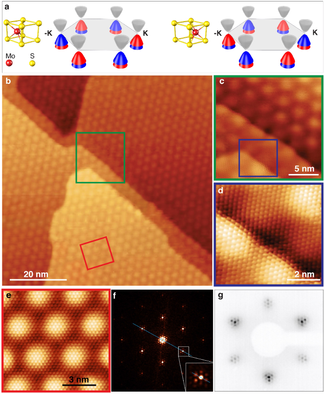
The overall structural properties of the resulting layer were characterized by scanning tunneling microscopy (STM) and low-energy electron diffraction (LEED). The STM images (Figure 1b, c and d) show a small-scale hexagonal atomic structure due to the top sulfur layer of the S-Mo-S structure of MoS2 together with a large scale moiré pattern due to the lattice mismatch between MoS2 and Au(111). The moiré superlattice is well visible on the Au terraces and maintains its orientation across the Au atomic steps. The atomically-resolved images acquired in the green- and blue-framed regions (Figure 6c and d, respectively) show that the MoS2 layer extends over the Au atomic steps with carpeting effect. The large area image (Figure 6b) evidences the lack of any domain boundaries or dislocations on the entire probed area ().
Fast-Fourier transform (FFT) analysis (figure 6f) was carried out on the representative atomically-resolved image measured on a Au terrace (Figure 6e). The alignment of the FFT spots as indicated by the blue line in the figure shows that the MoS2 layer is aligned along the direction of the moiré superstructure, and thus aligned along the crystallographic axes of the Au(111) substrate. This implies that only two orientations of the MoS2 layer are possible, rotated by 180∘ with respect to each other. This finding is at variance with respect to the results reported in literature for SL MoS2 grown with the earlier synthesis method Sorensen et al. (2014); Miwa et al. (2015a); Lauritsen et al. (2007), for which a misalignment angle of between the MoS2 and the Au substrate was observed Sorensen et al. (2014). Moreover, by comparing this outcome with the LEED (Figure 6g) and SPA-LEED patterns (see below) we can deduce that the moiré superstructure is due to the surface unit cell of MoS2 over the unit cell of Au(111).
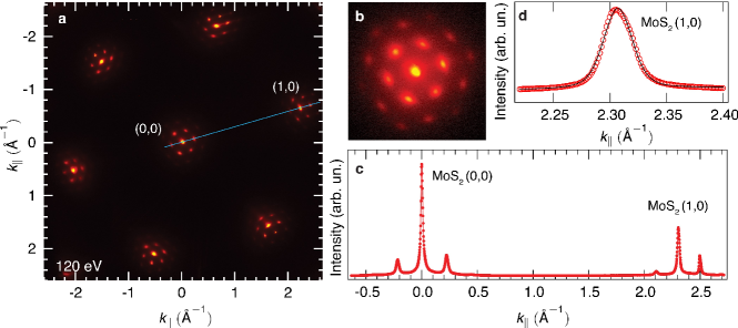
To measure the average domain size of the MoS2 layer we performed high-resolution -space measurements by means of spot-profile analysis (SPA)-LEED. The two-dimensional pattern measured at a kinetic energy of 120 eV is shown in Figure 2a. Besides the zeroth- and first-order spots, the image shows the appearance of additional diffraction spots due to the moiré superlattice. This can be appreciated in Figure 2b, where the k-space has been probed around the diffraction beam. The spot profile along the direction is presented in Figure 2c. The panel in Figure 2d shows a detail of the (1,0) MoS2 spot together with the best fit analysis obtained using a Voigt function. The Gaussian width is 0.0210 Å-1, while the Lorentzian full width at half maximum () is 0.0094 Å-1, corresponding to an average domain size of Å. Since this is comparable with the transfer width of the instrument, the average domain size could largely exceed this value.
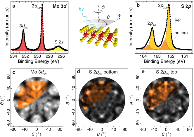
The high structural quality is also reflected in core level spectra obtained by XPS and shown in Figure 3a and b for Mo 3 and S 2, respectively. The Mo 3 spectrum can be fitted with a doublet (red) with the Mo 3 centered at 229.19 eV (spin-orbit splitting of 3.15 eV). The broad peak at 226.43 eV (yellow) is the S 2 core level. The S 2 core level shows two strong spin-orbit doublets Sorensen et al. (2014). The more intense peak at 162.15 eV (light orange) is assigned to the S 2 core level of the upper sulfur layer (i.e. the layer towards vacuum) and the weaker at 162.44 eV (dark orange) to the layer towards the Au surface. The width of these components (table S1) and the absence of additional peaks related to sulfided species not converted into MoS2 or to the atoms at the edges of the MoS2 islands Bruix et al. (2015) are indicative of the high quality of the layer, in accordance with the STM and LEED results.
The single orientation of the MoS2 layer can be ascertained in an x-ray photoelectron diffraction (XPD) experiment, as already successfully demonstrated for h-BNOrlando et al. (2014). This technique is based on emission-angle-dependent modulations of the core level photoemission intensity from the different atoms in the layer Woodruff (2007). The intensity modulations arise from the length difference between individual scattering pathways from the emitting atom to the detector and the coherent interference of the scattered waves. The XPD modulations are thus directly reflecting the local structural environment of the emitting atom.
Figure 3c, d and e show stereographic projections of the modulation function (see Methods) for Mo and the lower and upper S atoms, respectively. The colored part is the data and the greyscale part is a simulation for a layer with a single orientation (see below). The kinetic energy of the photoelectrons for the main XPS line in these experiments can be chosen by tuning the incoming photon energy; it was set high for the lower S atoms, favoring forward scattering processes from the Mo and S above, and low for the Mo and upper S atoms, favoring backscattering processes. All three diffraction patterns show a clear three-fold symmetry. Assuming a negligible influence of the underlying Au surface on the symmetry of the pattern, this already excludes the presence of equal areas of mirror domains, since these would give rise to a six-fold pattern.
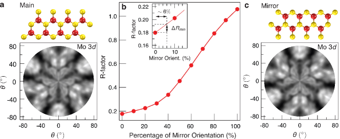
For further analysis, simulated diffraction patterns were calculated for the Mo of trial MoS2 structures using the software package for Electron Diffraction in Atomic Clusters (EDAC)García de Abajo et al. (2001). In these simulations the underlying Au surface was totally neglected, which is appropriate because of the lack of a specific local adsorption configuration of MoS2 on the substrate due to the lattice mismatch with Au(111). The orientation and the structure of SL MoS2 were determined by minimizing the Reliability () factor as a function of the abundance of the two possible orientations observed with STM, of the lattice parameter and of the S-S inter-plane separation. (see Supplementary Information for details). The total intensity in the simulated diffraction patterns for different admixtures of the two mirror orientations can be expressed as
| (1) |
being the contribution to the XPD pattern sourcing from the main orientation (Figure 4a) and the contribution from the mirror orientation (Figure 4c). As displayed in Figure 4b, the R-factor shows a minimum when only the main orientation is present, while the agreement is worsened for any admixture of the two orientations. We estimated the maximum amount of the mirror orientation consistent with our data by calculating the confidence interval displayed in the inset of Figure 3b (see Supplementary Information for details). Based on this analysis, we can infer that the fraction of the mirror orientation in the MoS2 layer does not exceed 6 %. These outcomes are consistent with the results stemming from the LEED pattern in Figure 6g showing a clear three-fold symmetry, although these observations alone would not be sufficient to establish the domain orientation, which can be conclusively determined by XPD. The single orientation growth on Au(111) is likely due to the symmetry breaking originating from the substrate. While the first atomic layer of Au(111) has a six-fold symmetry and would permit both MoS2 orientations, when the deeper Au layers are considered the crystal symmetry results to be three-fold. This apparently tips the balance between the two possible aligned orientations towards a single one. (See Supplementary Information for the details on the stacking registry between MoS2 and the Au(111) substrate)
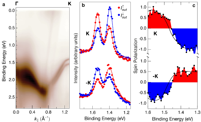
Having established the presence of a single domain orientation by analyzing the geometric structure of the layer, we proceed by demonstrating its effect on the electronic structure. Figure 5a shows the dispersion of the MoS2 bands measured by ARPES. The valence band maximum at is clearly visible, including the spin-orbit splitting of the state. As pointed out above, the band structure observed in an ARPES measurement without spin resolution is not substantially affected by the presence of mirror domains. Many small domains would merely lead to a spectral broadening due to defect scattering. While the data in Figure 5a are similar to previous findings for this system Miwa et al. (2015a); Bruix et al. (2016), the linewidth of the states near is substantially smaller (51 and 70 meV for the upper and lower band, respectively) than what reported earlier Miwa et al. (2015a), indicating a higher quality of the layer. The ARPES results show that the system has no detectable contributions from a second layer, as this would be observed as a second band near (see Supplementary for a detailed discussion about this issue).Zhang et al. (2014b); Miwa et al. (2015b)
The single orientation character of the layer can be expected to result in a complete spin polarization of the bands near and and Figure 5b and c show an experimental demonstration of this using spin-resolved photoemission spectroscopy. We find an out-of plane spin polarization of 8614%, which is opposite for and . In case of multiple-domain crystals, we expect the measured signal to be a mixture of contributions from oppositely spin-polarized and valleys, leading to a decreased value of spin polarization. Here, on the contrary, we measure a high magnitude of spin polarization, which further confirms the single domain orientation of the MoS2 monolayer.
Previous spin-resolved ARPES experiments on bulk TMDCs have revealed a surprising complexity in the observed spin texture. Naively, inversion symmetry should lead to no observable spin polarization from the 2H structural polymorph while the 3R polymorph could give rise to a spin-polarized signal. The latter was indeed found for 3R MoS2 Suzuki et al. (2014) while, surprisingly, also 2H WSe2 revealed strongly spin-polarized bands, essentially due to a combination of local symmetry breaking and surface sensitivity in photoemission Riley et al. (2014). Later, it was shown that the observed spin polarization from 2H MoS2 could even be switched by excitation with circularly polarized light of different handedness Razzoli et al. (2017). In simple terms, this effect is based on the coupling of the light to different valleys in the band structure and the locking of valley and layer degrees of freedom in the 2H structure. Such a switching effect, and more in general a strong dependence on photon energy and light polarization of the spin-polarization, should not be observable in the case of a single-orientation single layerRazzoli et al. (2017). This is confirmed by results for SL MoSe2 grown on bilayer graphene Mo et al. (2016): the spin polarization was not found to change significantly with photon energy, even if it is much smaller than the value reported here, due to the presence of mirror domains. However, due to the complexity of the spin-polarized photoemission process, changes of the observed polarization due to e.g. final state effects cannot be excluded. We thus emphasize that the observed spin polarization in our case is consistent with the presence of a single domain, but that our analysis of the domain distribution rests not on this but on the structural analysis based on XPD.
III Conclusions
In summary, we have presented a synthesis method to produce high quality, singly-oriented SL MoS2. We used a multi-method approach to determine the structural properties of the layer and we measured for the first time the complete spin polarization of the states near and of SL MoS2 by spin-resolved ARPES.
The synthesis method outlined here may represent a breakthrough for the large scale production of high-quality MoS2 monolayers with a low number of dislocation defects. The availability of the singly-oriented MoS2 monolayers obtained with this protocol may boost the research on the spin-valley degree of freedom in two-dimensional materials and could be the key to realize mass-produced devices based on the valleytronics concept. This growth protocol could potentially be applied also for the synthesis of high-quality singly-oriented WS2 or MoSe2 monolayers on Au(111). Guided by the developments in graphene synthesis, one could expect that this method can be employed on other substrates or that destruction-free transfer mechanisms for large areas can be devised.
IV Experimental Methods
The growth of MoS2 samples, the LEED, the high-resolution XPS and the XPD experiments were carried out at the SuperESCA beamline of the Elettra synchrotron radiation facility in Trieste (Italy) Baraldi et al. (2003). The UHV experimental chamber is equipped with a Phoibos hemispherical electron energy analyzer (150 mm mean radius), implemented with a home-made delay line detector. The experimental chamber is equipped also with a rear-view LEED system. The Au single crystal was fixed on a Ta plate and the sample temperature was measured by two thermocouples spot-welded very close to it. The sample holder was mounted on a 5 degrees of freedom (, , , , ) manipulator.
The Au(111) surface was prepared by repeated cycles of Ar+ sputtering followed by annealing up to 920 K for 10 min. The heating and cooling rate was 1 K/s. After the cleaning procedure, the sample cleanliness was checked with XPS, which did not detect any trace of contaminants within the detection limit of 0.1% of a monolayer (ML) where 1 ML corresponds to the surface atomic density of the Au(111) surface. The long-range order was verified by acquiring the LEED pattern on the freshly prepared sample, which showed the extra spots of the herringbone reconstruction.
MoS2 monolayers were grown by dosing molybdenum from a home-built evaporator, consisting of a Mo filament annealed through direct current heating, while keeping the Au substrate at 823 K and dosing H2S (nominal purity 99.8%) through a leak valve at background pressure of mbar. The Mo deposition rate was estimated by means of a quartz microbalance and amounted to ML/minute. Therefore, the total amount of Mo deposited in 8000 s was 0.67 ML. From the attenuation of the surface component of the Au 4 core level due to the presence of the MoS2 layer, we estimated a MoS2 coverage of 0.65 ML (1 ML corresponds here to one layer of MoS2 covering the whole surface). High-resolution S and Mo core level spectra were measured at room temperature on the as-grown MoS2 monolayer, using photon energies of 260 eV and 360 eV, respectively. The overall energy resolution was better than 50 meV. The surface normal, the incident beam, and the electron emission direction were all in the horizontal plane, with the angle between the photon beam and the electron energy analyser fixed at . The high resolution core level spectra were acquired at normal electron emission.
SPA-LEED measurements were carried out at the Surface Science Laboratory of Elettra Sincrotrone Trieste using a commercial Omicron SPA-LEED Lizzit et al. (2009). The transfer width was better than 1000 Å. The instrument was used to acquire two-dimensional diffraction patterns at fixed energy as well as to measure one-dimensional high-resolution profiles along specific reciprocal space directions. The line-profile of the diffraction spots were modeled with a Voigt function Locatelli et al. (2010). The Gaussian broadening accounts for the finite coherence length of the primary electron beam and for the corrugation of the substrate. The Lorentzian contribution is connected with the size of the MoS2 domains on the surface through the formula:
| (2) |
where is the full-width at half maximum of the Lorentzian component, and are the reciprocal and real lattice vectors of MoS2, respectively, and is the average width of the crystalline domains.
XPD patterns for Mo and S core levels were acquired with different photon energies () in order to change the corresponding electron kinetic energy (KE) to enhance forward and backscattering conditions. Specifically, Mo was acquired with eV corresponding to electron KE of 130 eV. The S XPD pattern from the top S layer was acquired at eV (electron KE of 108 eV) to enhance backscattering conditions, while the pattern from the bottom S layer was measured with eV (electron KE of 397 eV) to enhance forward scattering conditions. At each energy more than 1000 spectra were measured for different polar () and azimuthal () angles. For each of these spectra, the peak fit analysis was performed and the intensity , of each component resulting from the fit, i.e. the area under the photoemission line, was extracted. Each XPD pattern was measured over an azimuthal sector of , from normal () to grazing emission (), as shown in the sketch in the centre of Figure 3 of the main text. The resulting XPD patterns are the stereographic projection of the modulation function , which was obtained from the peak intensity for each polar emission angle as
| (3) |
where () is the average intensity for each azimuthal scan. The agreement between the simulations and the experimental results was quantified by computing the reliability factor (R),
| (4) |
where and are the calculated and the experimental modulation functions for each data point . The conformation of the MoS2 layer was determined by minimizing the R-factor upon variation of the structural parameters employed in the simulations Woodruff (2007). Following the determination of the minimum factor, a confidence interval for the result was estimated by using the approach inspired by the common practice in LEED Pendry (1980). The variance of the minimum -factor is calculated by
| (5) |
where is the number of well-resolved peaks in a LEED curve. Here we take , which is the approximate number of peaks in the 50 azimuthal scans acquired at different polar emission angles. Consequently, having we find .
ARPES experiments were carried out at the SGM-3 beamline of the synchrotron radiation facility ASTRID2 in Aarhus Hoffmann et al. (2004). The energy and angular resolution were better than 30 meV and 0.2∘, respectively. The sample temperature was 30 K. The sample was transferred to Aarhus in air. After inserting it into the ultrahigh vacuum system, it was annealed to 770 K to remove adsorbed impurities.
Spin-resolved ARPES measurements were taken at the APE beamline of Elettra Sincrotrone Trieste, Italy Bigi et al. (2017). The experimental chamber is equipped with a VG-Scienta DA30 analyzer and two very low energy electron diffraction (VLEED) spin polarimeters. Measurements were taken with a photon energy of 30 eV and p-polarized light, with the light incidence direction kept fixed at 45∘ with respect to the electron energy analyzer normal detection direction. The energy and angular resolution were better than 50 meV and 0.75∘, respectively. Samples were transferred into the chamber in air and subsequently annealed up to 800 K. Measurements were taken at about 80 K. Spin polarization was determined from spin-resolved energy dispersion curves (EDCs) :
| (6) |
where denotes the spin quantization axis in the reference frame of the detection and is the Sherman function of the detector. were corrected by a relative efficiency calibration and fitted with Gaussian-broadened Lorentzian (Voigt) peaks. The background contribution consisting of spin-unpolarized tails of lower-lying Au states was taken into account for the calculated spectra. Quantitative spin polarization magnitudes were determined from the area ratio of the fitted peaks. were transformed into the sample’s reference frame by applying an Euler’s rotation matrix.
STM measurements were carried out at the CoSMoS facility at Elettra Sincrotrone Trieste. The images were acquired at room temperature with a SPECS STM 150 Aarhus instrument equipped with a W tip. The samples were transferred through air from the growth chamber to the STM chamber, where they were subsequently annealed up to ca. 800 K for 30 min.
The size of the surface areas probed varied between the different experimental techniques. Light spots sizes for the synchrotron radiation experiments were typically in the order of more than 100 m, the electron beam size in SPA-LEED was about 100 m while for LEED was several hundreds micrometers. Most importantly, no spatial inhomogeneity or presence of a mirror domain was noted when probing different areas of the Au(111) crystal surface (several mm in diameter) with different techniques.
We thank David Abergel and Albert Bruix for stimulating discussions. This work was supported by the Danish Council for Independent Research, Natural Sciences under the Sapere Aude program (Grant No. DFF-4002-00029) and by VILLUM FONDEN via the Centre of Excellence for Dirac Materials (Grant No. 11744). Affiliation with the Center for Integrated Materials Research (iMAT) at Aarhus University is gratefully acknowledged.
V Supplementary Information
V.1 Tuning of the Growth Parameters by Fast XPS
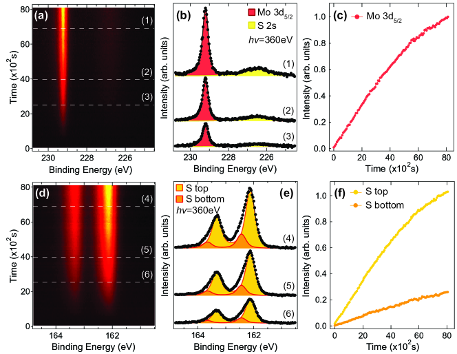
The careful tuning of the growth parameters was achieved by following the real time evolution of the MoS2 layer during the growth by means of fast-x-ray photoelectron spectroscopy (XPS) of the Mo and S core levels (Figure 6). In this way it was possible to avoid the growth of Mo clusters and partially sulfided species (core level peaks appearing at lower binding energy compared to those of MoS2), which did not convert into MoS2 even after prolonged annealing in H2S atmosphere without dosing Mo. As one can see in Figure S1(c) and (f), the MoS2 growth rate is constant until 2000 s and then it starts to decrease. This means that not all the Mo atoms react to form MoS2 when the surface coverage increases, because of the partial desorption, at high temperature, of the Mo atoms impinging on the already formed MoS2 layer.
V.2 Core Level Spectra Lineshape
| Mo (hv=360eV) | L (eV) | G (eV) | |
|---|---|---|---|
| 3 | 0.20 | 0.06 | 0.14 |
| 3 | 0.43 | 0.06 | 0.14 |
| S (hv=260eV) | L (eV) | G (eV) | |
| 2 top (bottom) | 0.18 (0.23) | 0.05 (0.02) | 0.16 (0.21) |
| 2 top (bottom) | 0.18 (0.23) | 0.05 (0.02) | 0.16 (0.21) |
The core level spectra were fitted using a Doniach-Šunjić line profile Doniach and Šunjić (1970) convoluted with a Gaussian broadening and a linear background. All binding energies presented in this work are referenced to the Fermi level of the Au substrate measured under the same experimental conditions. The fitting parameters for Mo and S core levels, for both top and bottom S, are listed in Table S1. The experimental error on the binding energy position of the peaks is meV.
V.3 MoS2 Monolayer vs Bilayer
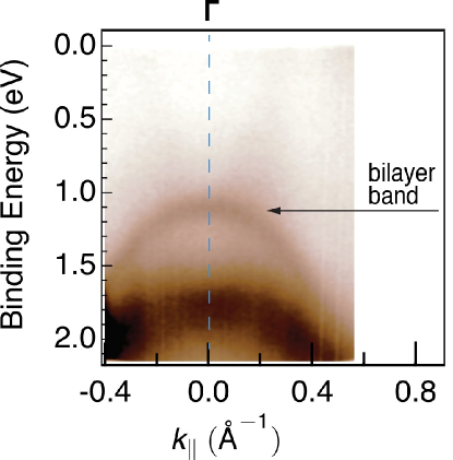
It is possible to ascertain the presence of regions on the Au surface covered by bilayer MoS2 by means of angle-resolved photoemission spectroscopy (ARPES), and thus discriminate samples where only monolayer is present. As earlier reported Miwa et al. (2015a, b); Grønborg et al. (2015), a second band at lower binding energy (BE) is visible at for MoS2 bilayer, while it appears to be completely absent for monolayer MoS2. In order to highlight these differences, we have grown a sample with a coverage exceeding 1 ML of MoS2, where bilayer areas are likely to be found Grønborg et al. (2015). An ARPES map acquired in the vicinity of the point of the Brillouin zone is shown in Figure 7. We can clearly see the appearance of a dispersing band centred at (pinpointed by an arrow) with the band maximum at about BE=1.1 eV. This feature is not present in the sample we employed for measurements described in the main paper (Figure 5), where the total MoS2 coverage was 0.65 ML. Hence, we can conclude that no apparent bilayer contamination is present for the monolayer MoS2 samples we have studied. STM analysis of the probed regions corroborated this conclusion, indicating that the possible presence of MoS2 bilayers would be limited to less than 1% of the sample surface.
V.4 Stacking of MoS2 on the Au substrate
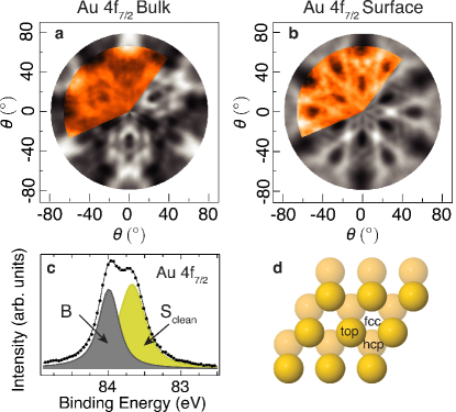
In order to determine the orientation of the Au(111) substrate, needed to identify the relative orientation of the MoS2 layer, we performed XPD measurements of the Au core level for the clean sample (Figure 8c). Figure 8a and b show the XPD patterns corresponding to the bulk (B) and clean surface () components (colored), respectively, measured at 200 eV photon energy (photoelectron kinetic energy eV). The XPD pattern of the bulk component shows the expected three-fold symmetry of the fcc crystal stacking, while the herringbone reconstruction presents an almost six-fold symmetry of the pattern from the Au surface component. For this reason the XPD pattern of the bulk peak provides the orientation of the Au substrate. The herringbone reconstruction was simulated by compressing the surface unit cell in the direction by 4.5%, averaging over the three rotated domains, while three layers below the surface were considered as the bulk. The experimental data show a good agreement (R-factor=0.33) with the simulations and the resulting orientation of the gold substrate was identified as shown in figure Figure 8d.
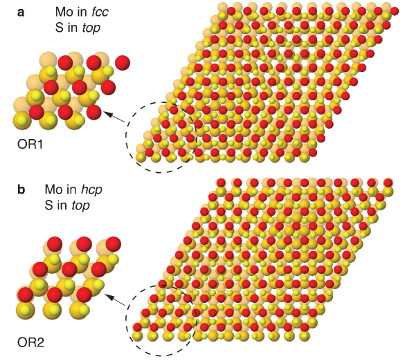
The MoS2 superstructure on Au unit cell for the two mirror domain orientations of MoS2 on Au, are shown in figure 9. Theoretical calculations by A. Bruix et al. Bruix et al. (2015) showed that the most favorable configuration for small 2D MoS2 clusters on Au(111) is with the S atoms in atop position. Looking at the left corner of the moiré unit cell displayed in Figure 9a and b, when the S atoms are in atop position, the Mo atoms can go in the three-fold fcc (OR1) or hcp (OR2) position. By combining the outcomes of the analysis of the XPD patterns stemming from Mo and S displayed in the main text (Figure 3) with the pattern acquired on the bulk component of Au , we can conclude that MoS2 is adsorbed on Au(111) with the OR1 configuration, having thus Mo in the fcc position.
V.5 R-factor analysis of the XPD patterns
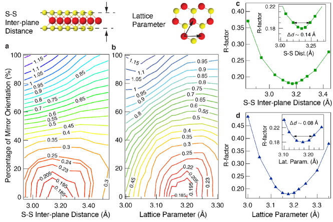
The structural conformation of the SL MoS2 was determined by comparing experimental and simulated XPD patterns, aiming to minimise the Reliability factor (R)Woodruff (2007). Systematic multiple scattering simulations of the Mo core level were performed as a function of the MoS2 lattice parameter, of the S-S inter-plane distance and of the percentage of the main (sketched in Figure 10) and of the mirror orientation in the layer. The initial guess for the values of the lattice parameter (3.16 Å) and for the S-S inter-plane lattice distance (3.17 Å) were assumed from results reported for the characteristic sizes of the MoS2 lattice Holinski and Gänsheimer (1972). In Figure 10a and b we show contour plots reporting the R-factor as a function of the percentage of mirror orientation and of the S-S inter-plane distance and lattice parameter, respectively. A clear minimum for the R-factor is observed when only the main orientation is included in the simulation for both plots.
Figure 10c and d report plots of the R-factor vs the S-S distance and the lattice parameter, respectively, for the singly-oriented layer (0% of the mirror orientation in Figure 10a and b). The minimum R-factor is obtained for a S-S inter-plane distance of Å and for a lattice parameter of Å. The errors on these dimensions were obtained through the confidence interval , as described in the Methods section Pendry (1980). These optimised distances were used to compute the diffraction patterns for S (Figure 1g and h in the main text), yielding R-factors of 0.25 and 0.15 for the upper and lower S atoms, respectively.
References
- Mak et al. (2012) K. F. Mak, K. He, J. Shan, and T. F. Heinz, Nat. Nanotech. 7, 494 (2012).
- Zeng et al. (2012) H. Zeng, J. Dai, W. Yao, D. Xiao, and X. Cui, Nat. Nanotech. 7, 490 (2012).
- Cao et al. (2012) T. Cao, G. Wang, W. Han, H. Ye, C. Zhu, J. Shi, Q. Niu, P. Tan, E. Wang, B. Liu, and J. Feng, Nat. Commun. 3, 887 (2012).
- Mak et al. (2014) K. F. Mak, K. L. McGill, J. Park, and P. L. McEuen, Science 344, 1489 (2014).
- Wang et al. (2017) Z. Wang, L. Zhao, K. F. Mak, and J. Shan, Nano Lett. 17, 740 (2017).
- Xiao et al. (2012) D. Xiao, G.-B. Liu, W. Feng, X. Xu, and W. Yao, Phys. Rev. Lett. 108, 196802 (2012).
- Xu et al. (2014) X. Xu, W. Yao, D. Xiao, and T. F. Heinz, Nature Phys. 10, 343 (2014).
- van der Zande et al. (2013) A. M. van der Zande, P. Y. Huang, D. A. Chenet, T. C. Berkelbach, Y. You, G.-H. Lee, T. F. Heinz, D. R. Reichman, D. A. Muller, and J. C. Hone, Nat. Mater. 12, 554 (2013).
- Zhou et al. (2013) W. Zhou, X. Zou, S. Najmaei, Z. Liu, Y. Shi, J. Kong, J. Lou, P. M. Ajayan, B. I. Yakobson, and J.-C. Idrobo, Nano Lett. 13, 2615 (2013).
- Najmaei et al. (2013) S. Najmaei, Z. Liu, W. Zhou, X. Zou, G. Shi, S. Lei, B. I. Yakobson, J.-C. Idrobo, P. M. Ajayan, and J. Lou, Nat Mater 12, 754 (2013).
- Mak et al. (2010) K. F. Mak, C. Lee, J. Hone, J. Shan, and T. F. Heinz, Phys. Rev. Lett. 105, 136805 (2010).
- Radisavljevic et al. (2011) B. Radisavljevic, A. Radenovic, J. Brivio, V. Giacometti, and A. Kis, Nat. Nanotech. 6, 147 (2011).
- Sarkar et al. (2015) D. Sarkar, X. Xie, W. Liu, W. Cao, J. Kang, Y. Gong, S. Kraemer, P. M. Ajayan, and K. Banerjee, Nature 526, 91 (2015).
- Dumcenco et al. (2015a) D. Dumcenco, D. Ovchinnikov, K. Marinov, P. Lazić, M. Gibertini, N. Marzari, O. L. Sanchez, Y.-C. Kung, D. Krasnozhon, M.-W. Chen, S. Bertolazzi, P. Gillet, A. F. i Morral, A. Radenovic, and A. Kis, ACS Nano 9, 4611 (2015a).
- Dumcenco et al. (2015b) D. Dumcenco, D. Ovchinnikov, O. L. Sanchez, P. Gillet, D. T. L. Alexander, S. Lazar, A. Radenovic, and A. Kis, 2D Materials 2, 044005 (2015b).
- Mak and Shan (2016) K. F. Mak and J. Shan, Nature Photonics 10, 216 (2016).
- Zhang et al. (2018) T. Zhang, Y. Wang, J. Xu, L. Chen, H. Zhu, Q. Sun, S. Ding, and D. W. Zhang, 2D Materials 5, 015028 (2018).
- Splendiani et al. (2010) A. Splendiani, L. Sun, Y. Zhang, T. Li, J. Kim, C.-Y. Chim, G. Galli, and F. Wang, Nano Lett. 10, 1271 (2010).
- Bernardi et al. (2013) M. Bernardi, M. Palummo, and J. C. Grossman, Nano Lett. 13, 3664 (2013).
- Gutiérrez et al. (2013) H. R. Gutiérrez, N. Perea-López, A. L. Elías, A. Berkdemir, B. Wang, R. Lv, F. López-Urías, V. H. Crespi, H. Terrones, and M. Terrones, Nano Lett. 13, 3447 (2013).
- Das et al. (2014) S. Das, A. Prakash, R. Salazar, and J. Appenzeller, ACS Nano 8, 1681 (2014).
- Lopez-Sanchez et al. (2013) O. Lopez-Sanchez, D. Lembke, M. Kayci, A. Radenovic, and A. Kis, Nat. Nanotech. 8, 497 (2013).
- Withers et al. (2015) F. Withers, O. Del Pozo-Zamudio, A. Mishchenko, A. P. Rooney, A. Gholinia, K. Watanabe, T. Taniguchi, S. J. Haigh, A. K. Geim, A. I. Tartakovskii, and K. S. Novoselov, Nat. Mater. 14, 301 (2015).
- Di Bartolomeo et al. (2018) A. Di Bartolomeo, L. Genovese, F. Giubileo, L. Iemmo, G. Luongo, T. Foller, and M. Schleberger, 2D Materials 5, 015014 (2018).
- Rycerz et al. (2007) A. Rycerz, J. Tworzydlo, and C. W. J. Beenakker, Nature Phys. 3, 172 (2007).
- Xiao et al. (2007) D. Xiao, W. Yao, and Q. Niu, Phys. Rev. Lett. 99, 236809 (2007).
- Zhang et al. (2014a) Y. J. Zhang, T. Oka, R. Suzuki, J. T. Ye, and Y. Iwasa, Science 344, 725 (2014a).
- Zhang et al. (2017) F. Zhang, K. Momeni, M. A. AlSaud, A. Azizi, M. F. Hainey Jr, J. M. Redwing, L.-Q. Chen, and N. Alem, 2D Materials 4, 025029 (2017).
- Shi et al. (2012) Y. Shi, W. Zhou, A.-Y. Lu, W. Fang, Y.-H. Lee, A. L. Hsu, S. M. Kim, K. K. Kim, H. Y. Yang, L.-J. Li, J.-C. Idrobo, and J. Kong, Nano Lett. 12, 2784 (2012).
- Fu et al. (2017) D. Fu, X. Zhao, Y.-Y. Zhang, L. Li, H. Xu, A.-R. Jang, S. I. Yoon, P. Song, S. M. Poh, T. Ren, Z. Ding, W. Fu, T. J. Shin, H. S. Shin, S. T. Pantelides, W. Zhou, and K. P. Loh, Journal of the American Chemical Society 139, 9392 (2017).
- Miwa et al. (2015a) J. A. Miwa, S. Ulstrup, S. G. Sørensen, M. Dendzik, A. G. Čabo, M. Bianchi, J. V. Lauritsen, and P. Hofmann, Phys. Rev. Lett. 114, 046802 (2015a).
- Lauritsen et al. (2007) J. V. Lauritsen, J. Kibsgaard, S. Helveg, H. Topsoe, B. S. Clausen, E. Laegsgaard, and F. Besenbacher, Nat. Nanotech. 2, 53 (2007).
- Ulstrup et al. (2017) S. Ulstrup, A. G. Čabo, D. Biswas, J. M. Riley, M. Dendzik, C. E. Sanders, M. Bianchi, C. Cacho, D. Matselyukh, R. T. Chapman, E. Springate, P. D. C. King, J. A. Miwa, and P. Hofmann, Phys. Rev. B 95, 041405 (2017).
- Sorensen et al. (2014) S. G. Sorensen, H. G. Füchtbauer, A. K. Tuxen, A. S. Walton, and J. V. Lauritsen, ACS Nano 8, 6788 (2014).
- Bruix et al. (2015) A. Bruix, H. G. Füchtbauer, A. K. Tuxen, A. S. Walton, M. Andersen, S. Porsgaard, F. Besenbacher, B. Hammer, and J. V. Lauritsen, ACS Nano 9, 9322 (2015).
- Orlando et al. (2014) F. Orlando, P. Lacovig, L. Omiciuolo, N. G. Apostol, R. Larciprete, A. Baraldi, and S. Lizzit, ACS Nano 8, 12063 (2014).
- Woodruff (2007) D. Woodruff, Surf. Sci. Rep. 62, 1 (2007).
- García de Abajo et al. (2001) F. J. García de Abajo, M. A. Van Hove, and C. S. Fadley, Phys. Rev. B 63, 075404 (2001).
- Bruix et al. (2016) A. Bruix, J. A. Miwa, N. Hauptmann, D. Wegner, S. Ulstrup, S. S. Grønborg, C. E. Sanders, M. Dendzik, A. G. Čabo, M. Bianchi, J. V. Lauritsen, A. A. Khajetoorians, B. Hammer, and P. Hofmann, Phys. Rev. B 93, 165422 (2016).
- Zhang et al. (2014b) Y. Zhang, T.-R. Chang, B. Zhou, Y.-T. Cui, H. Yan, Z. Liu, F. Schmitt, J. Lee, R. Moore, Y. Chen, H. Lin, H.-T. Jeng, S.-K. Mo, Z. Hussain, A. Bansil, and Z.-X. Shen, Nat. Nanotech. 9, 111 (2014b).
- Miwa et al. (2015b) J. A. Miwa, M. Dendzik, S. S. Grønborg, M. Bianchi, J. V. Lauritsen, P. Hofmann, and S. Ulstrup, ACS Nano 9, 6502 (2015b).
- Suzuki et al. (2014) R. Suzuki, M. Sakano, Y. J. Zhang, R. Akashi, D. Morikawa, A. Harasawa, K. Yaji, K. Kuroda, K. Miyamoto, T. Okuda, K. Ishizaka, R. Arita, and Y. Iwasa, Nat. Nanotech. 9, 611 (2014).
- Riley et al. (2014) J. M. Riley, F. Mazzola, M. Dendzik, M. Michiardi, T. Takayama, L. Bawden, C. Granerod, M. Leandersson, T. Balasubramanian, M. Hoesch, T. K. Kim, H. Takagi, W. Meevasana, P. Hofmann, M. S. Bahramy, J. W. Wells, and P. D. C. King, Nat. Phys. 10, 835 (2014).
- Razzoli et al. (2017) E. Razzoli, T. Jaouen, M.-L. Mottas, B. Hildebrand, G. Monney, A. Pisoni, S. Muff, M. Fanciulli, N. C. Plumb, V. A. Rogalev, V. N. Strocov, J. Mesot, M. Shi, J. H. Dil, H. Beck, and P. Aebi, Phys. Rev. Lett. 118, 086402 (2017).
- Mo et al. (2016) S.-K. Mo, C. Hwang, Y. Zhang, M. Fanciulli, S. Muff, J. H. Dil, Z.-X. Shen, and Z. Hussain, Journal of Physics: Condensed Matter 28, 454001 (2016).
- Baraldi et al. (2003) A. Baraldi, G. Comelli, S. Lizzit, M. Kiskinova, and G. Paolucci, Surf. Sci. Rep. 49, 169 (2003).
- Lizzit et al. (2009) S. Lizzit, A. Baraldi, C. Grütter, J. Bilgram, and P. Hofmann, Surf. Sci. 603, 3222 (2009).
- Locatelli et al. (2010) A. Locatelli, K. R. Knox, D. Cvetko, T. O. Menteş, M. A. Niño, S. Wang, M. B. Yilmaz, P. Kim, R. M. Osgood, and A. Morgante, ACS Nano 4, 4879 (2010).
- Pendry (1980) J. B. Pendry, Journal of Physics C: Solid State Physics 13, 937 (1980).
- Hoffmann et al. (2004) S. V. Hoffmann, C. Søndergaard, C. Schultz, Z. Li, and P. Hofmann, Nucl. Instr. Meth. Phys. Res. A 523, 441 (2004).
- Bigi et al. (2017) C. Bigi, P. K. Das, D. Benedetti, F. Salvador, D. Krizmancic, R. Sergo, A. Martin, G. Panaccione, G. Rossi, J. Fujii, I. Vobornik, and IUCr, Journal of Synchrotron Radiation 24, 750 (2017).
- Doniach and Šunjić (1970) S. Doniach and M. Šunjić, J. Phys.C 3, 285 (1970).
- Grønborg et al. (2015) S. S. Grønborg, S. Ulstrup, M. Bianchi, M. Dendzik, C. E. Sanders, J. V. Lauritsen, P. Hofmann, and J. A. Miwa, Langmuir 31, 9700 (2015).
- Holinski and Gänsheimer (1972) R. Holinski and J. Gänsheimer, Wear 19, 329 (1972).