High Kinetic Inductance NbN Nanowire Superinductors
Abstract
We demonstrate that a high kinetic inductance disordered superconductor can realize a low microwave loss, non-dissipative circuit element with an impedance greater than the quantum resistance (). This element, known as a superinductor, can produce a quantum circuit where charge fluctuations are suppressed. The superinductor consists of a wide niobium nitride nanowire and exhibits a single photon quality factor of . Furthermore, by examining loss rates, we demonstrate that the dissipation of our nanowire devices can be fully understood in the framework of two-level system loss.
Disorder within superconductors can reveal non-trivial electrodynamics Driessen et al. (2012); Mondal et al. (2011), dual Josephson effects Astafiev et al. (2012), and superconducting-insulating phase transitions (SIT) Haviland et al. (1989). In general, the disorder increases the superconductors’ normal-state resistance, which also enhances the kinetic inductance. High kinetic inductance can be used to produce circuits with impedances exceeding the resistance quantum (). A quantum circuit element with zero dc resistance, low microwave losses and an impedance above is known as a superinductor Masluk et al. (2012); Bell et al. (2012). Qubits based on superinductors are immune to charge fluctuations and have demonstrated extraordinary relaxation times Pop et al. (2014). However, these examples of superinductors have been based on the kinetic inductance of Josephson junction arrays (JJA), which places constraints on the possible device parameters and geometries. Therefore, there remains interest in a superinductor formed by a disordered superconducting nanowire Kerman (2010).
A disordered superconductor-based superinductor should possess tremendous magnetic field tolerance Samkharadze et al. (2016), suitable for hybrid qubits which operate at high magnetic fields Luthi et al. (2017). To fully exploit these circuits, more work is needed to understand and mitigate sources of unconventional dissipation relating to the proximity to the SIT Coumou et al. (2013); Feigel’man and Ioffe (2018). This motivates the need to fabricate a sufficiently disordered superconductor to obtain high inductance, but not so disordered as to induce dissipation. Therefore, to maximize impedance, it becomes crucial to minimize the stray capacitance, which can be achieved with a nanowire geometry. However, while low-loss superconducting nanowires can be fabricated Burnett et al. (2017), the nanowire geometry is itself more susceptible to parasitic two-level systems (TLS). This susceptibility is due to an enhanced participation ratio Gao et al. (2008) of the TLS host volume to the total volume threaded by the electric field. It is due to these loss mechanisms that present superinductor circuits have preferred JJAs Masluk et al. (2012) rather than disordered superconductors.
Here, we demonstrate a nanowire-based superinductor with an impedance of . We developed a process Not based on dry etching a hydrogen silsesquioxane (HSQ) mask to pattern a thick, strongly disordered film of niobium nitride (NbN) into a wide and long nanowire. These dimensions ensure a large inductance while exponentially suppressing unwanted phase slips in our devices Not ; Peltonen et al. (2013). We study both the microwave transmission and dc transport properties of several nanowires to characterize their impedance and microwave losses. These nanowire-based superinductors demonstrate a single photon quality factor of , which is comparable to JJA-based superinductors Masluk et al. (2012). We find that the dominant loss mechanism is parasitic two level systems (TLS), which is exacerbated by the unfavorable TLS filling factor Gao et al. (2008) that arises from the small dimensions required to obtain a high impedance.
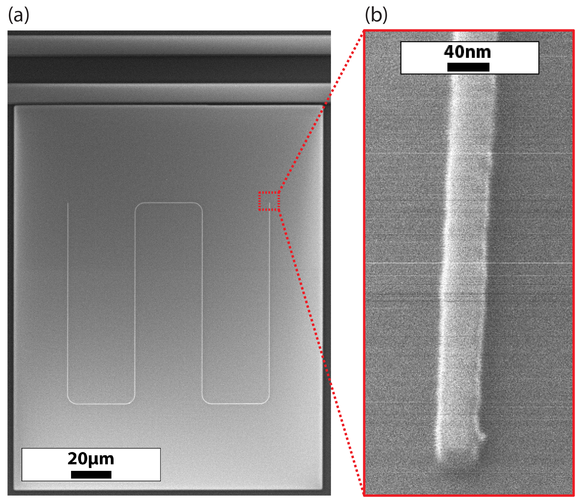
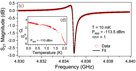
The final sample contains five nanowires that are inductively coupled to a common microwave transmission line. The sample also contains separate dc transport test structures. Figure 1(a–b) show micrographs of a typical device. We study the microwave properties of these resonators by measuring the forward transmission () response. Figure 1(c) shows a typical magnitude response measured at and with an average photon population . We determine the resonator parameters by fitting the data with a traceable fit routine Probst et al. (2015). From this we find a resonant frequency and an internal quality factor .
To understand this resonance, we first study the transport properties of our NbN nanowires. We estimate the kinetic inductance contribution using Tinkham (2004)
| (1) |
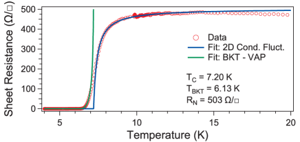
where is the normal-state sheet resistance, the reduced Planck constant, and the superconducting gap at zero temperature. NbN is experimentally found to be a strongly coupled superconductor with Mondal et al. (2011), where is the critical temperature and is the Boltzmann constant. Figure 2 shows a typical characteristic of an NbN nanowire. From room temperature, as the temperature decreases, the resistance increases until a plateau is reached at about . This behavior is typical of weak localization in strongly disordered materials Bergmann (1983). As the temperature further decreases from , the resistance starts to decrease and we observe a wide superconducting transition.
The width of this superconducting transition can be fully described by two different mechanisms. Above , thermodynamic fluctuations give rise to short-lived Cooper pairs, which increase the conductivity. These conductivity fluctuations have been described in the 2D case by Aslamasov and Larkin Tinkham (2004) and are given by
| (2) |
where is the temperature, is the electron charge and is the film thickness. The total conductivity above is now expressed as .
Below , the resistance does not immediately vanish. This can be explained by a Berezinskii–Kosterlitz–Thouless (BKT) transition Mooij (1984) where thermal fluctuations excite pairs of vortices. These vortex-antivortex pairs (VAP) are bound states, formed by vortices with supercurrents circulating in opposite directions. Above the ordering temperature , VAPs start to dissociate and their movement cause the observed finite resistance. This resistivity is described by Mooij (1984)
| (3) |
with , and where are material dependent parameters.
Fitting the of Figure 2 to Eqs. (2–3) leads to and . Using Eq. (1), this yields . For a wide nanowire this corresponds to an inductance per unit length of . From an empirical formula Mohan et al. (1999), the magnetic inductance, due to the geometry of the nanowire, is estimated to be only . Therefore, we assume the nanowire inductance arises entirely from the kinetic inductance, so that . Using Sonnet em microwave simulator, we estimate the capacitance per unit length of our nanowires to be . Combining these properties leads to an estimated resonance frequency within 1% of the measured resonance frequencies of our resonators. Using these parameters, we calculate the characteristic impedance of our nanowires to be . Therefore, , indicating that our nanowires are superinductors.
Having demonstrated superinductors, we now examine their behavior as a function of applied microwave drive and varying temperature. We first determine the range of temperatures at which we can operate our device. Figure 1(d) shows a measurement of the internal quality factor against temperature. We show that from to , the quality factor only marginally decreases from to . This offers a far greater range of operation than aluminum JJA-based superinductors, which show significant dissipation above 100 mKMasluk et al. (2012).
We now investigate the low-temperature loss mechanisms as a function of microwave power. When probed with an applied power , the average energy stored in a resonator of characteristic impedance is given by , where , and are respectively the coupling and loaded quality factors of the resonator. In the following, we describe the microwave power in , the average number of photons in the resonator, given by where is the Planck constant.
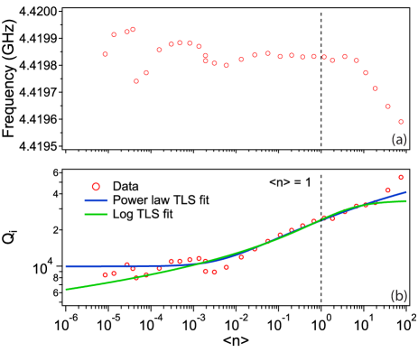
Due to the large impedance of our resonator, we are able to measure in the low photon regime with a high applied power. Consequently, this enables us to measure, with good signal-to-noise ratio, photon populations two to three orders of magnitude lower than in conventional resonators. In Figure 3(a), starting at , as we increase power, the resonance frequency does not change until . From , as power increases, the frequency decreases until the resonator bifurcates. This is explained by the power dependence of the kinetic inductance, which behaves as a Duffing-like non-linearity Swenson et al. (2013). We note that this non-linearity occurs at similar microwave drives as junctions-embedded resonators Osborn et al. (2007). Starting again at , as we decrease power, we see the frequency remain approximately constant. Although, as is decreased below , the resonator exhibits frequency jitter, consistent with TLS-induced permittivity changesBurnett et al. (2014). This frequency noise results in spectral broadening of the resonance curve.
We now examine the internal quality factor as a function of applied microwave power (shown in Figure 3(b)). Between the range of and , we find that is approximately constant, with changes in caused by frequency jitter-induced spectral broadening. From , as we increase power, increases, which is consistent with depolarization of TLS. For , is overestimated due to the Duffing non-linearity. We fit our data to a common TLS loss model Burnett et al. (2017) described by
| (4) |
where is the number of photons equivalent to the saturation field of the TLS, is the next dominant loss rate, and the filling factor is the ratio of electric field threading TLS to the total electric field. is the TLS loss tangent which is sensitive to a narrow spectrum of resonant TLS. Finally, describes the strength of TLS saturation with power. Early TLS theory suggests , however, recent results Burnett et al. (2014, 2017); Kirsh et al. (2017); de Graaf et al. (2017) commonly find a weaker scaling and associate it to a breakdown of the model described by Eq. (4) due to interactions between TLS. Therefore, we allow to be a fit parameter initialized to . We find (see Table 1).
| NW | ||||
|---|---|---|---|---|
| () | () | () | ||
| 4420 | 0.198 | 8.81 | 4.37 | 0.195 |
| 4562 | 0.196 | 7.51 | 3.84 | 0.183 |
| 4685 | 0.187 | 10.7 | 3.53 | 0.218 |
| 4837 | 0.180 | 8.24 | 4.40 | 0.153 |
| 5285 | 0.184 | 10.8 | 4.12 | 0.213 |
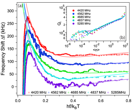
The intrinsic TLS loss tangent Gao et al. (2008), which is sensitive to the complete TLS spectrum, can be unambiguously determined using a Pound frequency-locked loop (P-FLL)Burnett et al. (2014); de Graaf et al. (2017). The P-FLL continuously tracks frequency changes of the resonator against temperature 111see Supplemental Material for details of the experimental setup. Figure 4(a) shows the changes in resonance frequency against the natural energy scale of the TLS (). The frequency shift Gao et al. (2008) is described by
| (5) |
where , , is a reference temperature and is the complex digamma function. Importantly, Eq. (5) only fits the TLS contribution but does not fit the temperature-dependent kinetic inductance contribution which occurs below .
We use Eq. (5) to fit the measured data. The resulting values of can be found in Table 1. We note that and differ by a factor 2 to 3, which is significantly larger than the difference typically observed Burnett et al. (2017). However, this is not unexpected as the low value of indicated that we are outside of the range of validity of Eq. (4)Burnett et al. (2017); de Graaf et al. (2017). The intrinsic loss tangent can be used to fit the data in Figure 3 using a model that takes TLS interactions into account Faoro and Ioffe (2015); Burnett et al. (2014).
| (6) |
where is a large constant, is the log-scaled next dominant loss rate and is the TLS switching rate ratio, defined by where and are the maximum and minimum rate of TLS switching respectively. These rates have been measured in the TLS-related charge-noise spectrum of single-electron transistors. They were found to extend from to Kafanov et al. (2008). This corresponds to . Our fitted values of are summarized in Table 1: we find values between and , in good agreement with this estimate and other results Burnett et al. (2016); Kirsh et al. (2017); de Graaf et al. (2017).
We have demonstrated that dissipation in our nanowires is not an intrinsic property of disorder within the filmCoumou et al. (2013); Feigel’man and Ioffe (2018) but is instead caused by TLS. This is not surprising as TLS are the predominant source of dissipation and decoherence in a wide variety of quantum devices. An important consequence of this is the role of the TLS filling factor. The ratio of E field threading TLS to the total E field is known to scale as approximately Gao et al. (2008), where is the center conductor width of a superconducting resonator. Consequently, the 40 nm width used here to produce a superinductor leads to an unfavorable filling factor and therefore a much lower than is found for wider superconducting resonator geometries. Additionally, the nanowire lithography relies on the use of a spin-on glass resist (HSQ) which resembles amorphous silicon oxide. Silicon oxide is a well-known host of TLS Barends et al. (2008) and because some HSQ remains unetched atop our nanowires, we suspect this is the dominant source of TLS in our devices. Therefore, improvements to the fabrication, specifically the non-trivial removal of the HSQ mask should result in significant improvements in device performance.
In conclusion, we have demonstrated a nanowire superinductance with an impedance of and a single photon quality factor of . This quality factor is comparable to both JJA-based superinductorsMasluk et al. (2012) and the tanh-scaled TLS loss in similar nanowire-resonatorsSamkharadze et al. (2016). We have analyzed the loss mechanisms in our devices and find TLS to be the dominant cause of loss, which is in contrast to the high rates of dissipation found in other nanowireAstafiev et al. (2012); Peltonen et al. (2013) or strongly disordered thin film devices Coumou et al. (2013). We emphasize that demonstrating nanowires losses are “conventional” is a important step forward for all nanowire-based quantum circuits. Therefore, this enables the possibility of long-lived nanowire-based superconducting circuits, such as a nanowire fluxonium qubitPop et al. (2014); Kerman (2010) or improved phase-slip qubits Astafiev et al. (2012); Peltonen et al. (2013). These high inductance and high impedance circuits can also be used as photon detectors Gao et al. (2008) or for exploring fundamental physics such as Bloch oscillations of charge for metrology applications Guichard and Hekking (2010), or for increasing zero-point fluctuations for detection applications Samkharadze et al. (2016).
Acknowledgements.
The authors thank O. W. Kennedy for He FIB imaging of our devices. We acknowledge useful discussions with S. E. Kubatkin, A. V. Danilov, and P. Delsing as well as support from the Chalmers Nanofabrication Laboratory staff. This research has been supported by funding from the Swedish Research Council and Chalmers Area of Advance Nanotechnology.References
- Driessen et al. (2012) E. F. C. Driessen, P. C. J. J. Coumou, R. R. Tromp, P. J. de Visser, and T. M. Klapwijk, Phys. Rev. Lett. 109, 107003 (2012).
- Mondal et al. (2011) M. Mondal, A. Kamlapure, M. Chand, G. Saraswat, S. Kumar, J. Jesudasan, L. Benfatto, V. Tripathi, and P. Raychaudhuri, Phys. Rev. Lett. 106, 047001 (2011).
- Astafiev et al. (2012) O. Astafiev, L. Ioffe, S. Kafanov, Y. A. Pashkin, K. Y. Arutyunov, D. Shahar, O. Cohen, and J. Tsai, Nature 484, 355 (2012).
- Haviland et al. (1989) D. B. Haviland, Y. Liu, and A. M. Goldman, Phys. Rev. Lett. 62, 2180 (1989).
- Masluk et al. (2012) N. A. Masluk, I. M. Pop, A. Kamal, Z. K. Minev, and M. H. Devoret, Phys. Rev. Lett. 109, 137002 (2012).
- Bell et al. (2012) M. T. Bell, I. A. Sadovskyy, L. B. Ioffe, A. Y. Kitaev, and M. E. Gershenson, Phys. Rev. Lett. 109, 137003 (2012).
- Pop et al. (2014) I. M. Pop, K. Geerlings, G. Catelani, R. J. Schoelkopf, L. I. Glazman, and M. H. Devoret, Nature 508, 369+ (2014).
- Kerman (2010) A. J. Kerman, Phys. Rev. Lett. 104, 027002 (2010).
- Samkharadze et al. (2016) N. Samkharadze, A. Bruno, P. Scarlino, G. Zheng, D. DiVincenzo, L. DiCarlo, and L. Vandersypen, Phys. Rev. Appl. 5, 044004 (2016).
- Luthi et al. (2017) F. Luthi, T. Stavenga, O. Enzing, A. Bruno, C. Dickel, N. Langford, M. Rol, T. Jespersen, J. Nygard, P. Krogstrup, et al., arXiv preprint arXiv:1711.07961 (2017).
- Coumou et al. (2013) P. Coumou, M. Zuiddam, E. Driessen, P. de Visser, J. Baselmans, and T. Klapwijk, IEEE T. Appl. Supercon. 23, 7500404 (2013).
- Feigel’man and Ioffe (2018) M. V. Feigel’man and L. B. Ioffe, Phys. Rev. Lett. 120, 037004 (2018).
- Burnett et al. (2017) J. Burnett, J. Sagar, O. W. Kennedy, P. A. Warburton, and J. C. Fenton, Phys. Rev. Appl. 8, 014039 (2017).
- Gao et al. (2008) J. Gao, M. Daal, A. Vayonakis, S. Kumar, J. Zmuidzinas, B. Sadoulet, B. A. Mazin, P. K. Day, and H. G. Leduc, Appl. Phys. Lett. 92, 152505 (2008).
- (15) See Supplemental Material.
- Peltonen et al. (2013) J. T. Peltonen, O. V. Astafiev, Y. P. Korneeva, B. M. Voronov, A. A. Korneev, I. M. Charaev, A. V. Semenov, G. N. Golt’sman, L. B. Ioffe, T. M. Klapwijk, and J. S. Tsai, Phys. Rev. B 88, 220506 (2013).
- Probst et al. (2015) S. Probst, F. B. Song, P. A. Bushev, A. V. Ustinov, and M. Weides, Rev. Sci. Instrum. 86, 024706 (2015).
- Tinkham (2004) M. Tinkham, Introduction to Superconductivity (Dover Books, 2004).
- Bergmann (1983) G. Bergmann, Phys. Rev. B 28, 2914 (1983).
- Mooij (1984) J. E. Mooij, Percolation, Localization and Superconductivity (Plenum Press, 1984).
- Mohan et al. (1999) S. S. Mohan, M. del Mar Hershenson, S. P. Boyd, and T. H. Lee, IEEE J. Solid-St. Circ. 34, 1419 (1999).
- Swenson et al. (2013) L. J. Swenson, P. K. Day, B. H. Eom, H. G. Leduc, N. Llombart, C. M. McKenney, O. Noroozian, and J. Zmuidzinas, J. Appl. Phys. 113, 104501 (2013).
- Osborn et al. (2007) K. D. Osborn, J. A. Strong, A. J. Sirois, and R. W. Simmonds, IEEE T. Appl. Supercond. 17, 166 (2007).
- Burnett et al. (2014) J. Burnett, L. Faoro, I. Wisby, V. L. Gurtovoi, A. V. Chernykh, G. M. Mikhailov, V. A. Tulin, R. Shaikhaidarov, V. Antonov, P. J. Meeson, A. Y. Tzalenchuk, and T. Lindström, Nat. Commun. 5, 4119 (2014).
- Kirsh et al. (2017) N. Kirsh, E. Svetitsky, A. L. Burin, M. Schechter, and N. Katz, Phys. Rev. Mat. 1, 012601 (2017).
- de Graaf et al. (2017) S. de Graaf, L. Faoro, J. Burnett, A. Adamyan, A. Y. Tzalenchuk, S. Kubatkin, T. Lindström, and A. Danilov, arXiv preprint arXiv:1705.09158 (2017).
- Note (1) See Supplemental Material for details of the experimental setup.
- Faoro and Ioffe (2015) L. Faoro and L. B. Ioffe, Phys. Rev. B 91, 014201 (2015).
- Kafanov et al. (2008) S. Kafanov, H. Brenning, T. Duty, and P. Delsing, Phys. Rev. B 78, 125411 (2008).
- Burnett et al. (2016) J. Burnett, L. Faoro, and T. Lindström, Supercond. Sci. Tech. 29, 044008 (2016).
- Barends et al. (2008) R. Barends, H. L. Hortensius, T. Zijlstra, J. J. A. Baselmans, S. J. C. Yates, J. R. Gao, and T. M. Klapwijk, Appl. Phys. Lett. 92, 223502 (2008).
- Guichard and Hekking (2010) W. Guichard and F. W. J. Hekking, Phys. Rev. B 81, 064508 (2010).
Supplemental Material
I Sample Fabrication
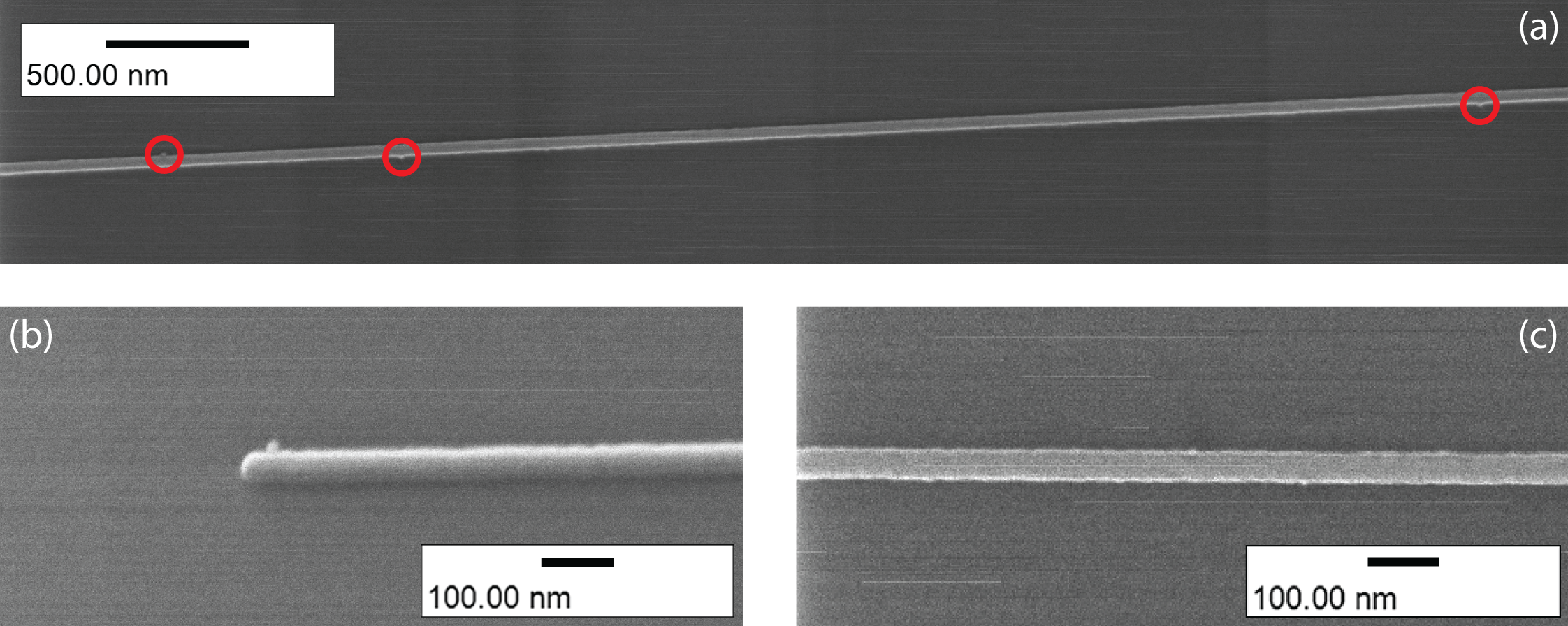
Samples are fabricated on high-resistivity () (100) intrinsic silicon substrates. Before processing, the substrate is dipped for in hydrofluoric acid (HF) to remove any surface oxide. Within , the wafer is loaded into a UHV sputtering chamber where a thick NbN thin film is deposited by reactive DC magnetron sputtering from a pure Nb target in a 6:1 Ar:N atmosphere. A -thick layer of PMMA A6 resist is spin-coated and then exposed with electron beam lithography (EBL) to define the microwave circuitry. After development, the pattern is transferred to the film by reactive ion etching (RIE) in a 50:4 Ar:Cl plasma at and . The nanowires are patterned in a subsequent EBL exposure using a layer of hydrogen silsesquioxane (HSQ), an ultra-high resolution negative resist suitable for features Chen et al. (2006).
A common problem with HSQ is the formation of small agglomerates that are not completely dissolved during development. These small particles tend to accumulate on the edges of developed structures and act as micro-masks when the pattern is etched. From FIB micrographs of our devices (see figure S1), we estimate a lithographic defect rate less than 3 defects per and that each defect contributes to the geometry of the device as approximately one square. For a long and nanowire, this translates to an uncertainty upper bound of , which is consistent with the 1% error reported in the main text.
II Exponentially suppressed phase slip rate
In the main text, we make the argument that the device dimensions are chosen to exponentially suppress phase slips. We estimate the phase slip rate for our device within the phenomenological model for strongly disordered superconductors. Our analysis is similar to that of Peltonen et al. Peltonen et al. (2013). In this model, is the phase slip energy and we have , where and are the nanowire length and average width respectively, represents the superfluid stiffness, , and is the Cooper pair density of states with .
For our device parameters (summarized in table S1), we find .
| Parameter | Symbol | Value |
|---|---|---|
| Normal state sheet resistance | ||
| Sheet kinetic inductance | ||
| Nanowire length | ||
| Nanowire width |
III Measurement Setup
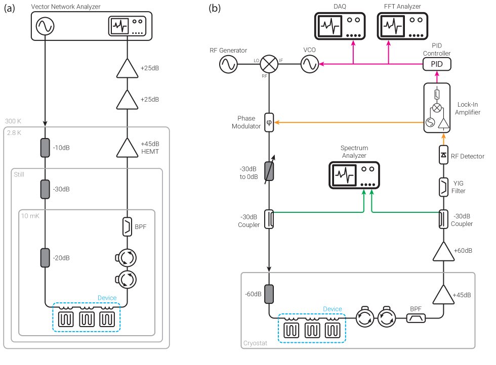
The sample is wire-bonded in a connectorized copper sample-box that is mounted onto the mixing chamber stage of a Bluefors LD250 dilution refrigerator (Fig. S2a). The inbound microwave signal is attenuated at each temperature stage by a total of before reaching the device under test. Accounting for cable losses and sample-box insertion loss, the total attenuation of the signal reaching the sample is . To avoid any parasitic reflections and noise leakage from amplifiers, the transmitted signal is fed through two microwave circulators (Raditek RADI-4.0-8.0-Cryo-4-77K-1WR) and a 4-8 band pass filter. Finally, the signal is amplified by a LNF LNC4_8A HEMT cryogenic amplifier ( gain) installed on the stage. Additional amplification is done at room temperature (Pasternack PE-1522 gain block amplifiers).
This microwave setup is connected to a vector network analyzer (Keysight PNA-X N5249A or R&S ZNB20) for initial characterization and quality factor measurements of the nanowire resonators at various excitation powers (Fig. S2a). However, as highlighted in the main text, at low drive powers, VNA measurements require significant amounts of averaging to increase the signal-to-noise ratio (SNR). At low microwave energies, frequency jitter leads to spectral broadening.
To reliably determine the TLS loss contribution, we instead measure the resonance frequency of the resonator against temperature Gao et al. (2008); Lindström et al. (2009). For that purpose, the microwave setup is included in a frequency locked loop using the so-called Pound locking technique (Fig. S2b). Originally developed for microwave oscillators Pound (1946), this technique is commonly used in optics for frequency stabilization of lasers Black (2001) and has been recently used for noise Lindström et al. (2009, 2011) and ESR de Graaf et al. (2012, 2017) measurements with superconducting microwave resonators. In this method, a carrier signal is generated by mixing the output of a microwave source (Keysight E8257D) and a VCO (Keysight 33622A). This carrier is phase-modulated (Analog Devices HMC538) before being passed through the resonator under test. The phase modulation frequency is set so that the sidebands are not interacting with the resonator. After amplification, the signal is filtered (MicroLambda MLBFP-64008) to remove the unwanted mixer image and rectified using an RF detector diode (Pasternack PE8016). The diode output is demodulated with a lock-in amplifier (Zurich Instruments HF2LI).
The feedback loop consist of an analog PID controller (SRS SIM960) locked on the zero-crossing of the error signal. This gives an output directly proportional to any shift in resonance frequency of the resonator. This output signal is then used to drive the frequency modulation of the VCO, varying its frequency accordingly and enabling the loop to be locked on the resonator.
In this work, we only sample the PID output slowly () to track frequency changes (Keithley 2000), but noise in the resonator can also be studied using a frequency counter (Keysight 53132A), a fast-sampling DAQ (NI PXI-6259 DAQ) or an FFT analyser (Keysight 35670A). This will be the focus of future work.
IV Geometrical considerations for nanowire superinductors
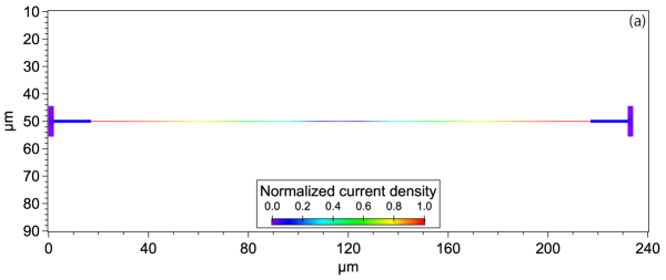
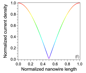
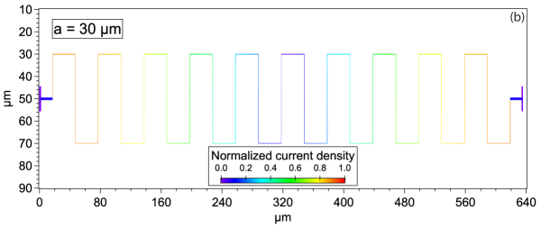
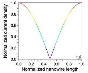
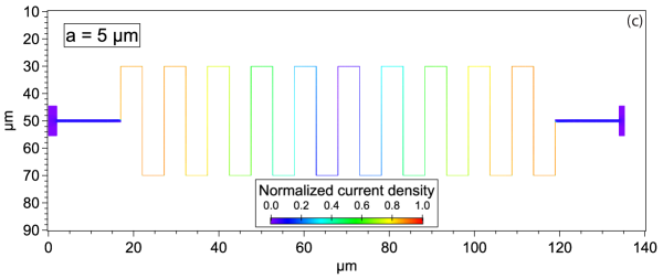
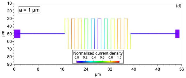
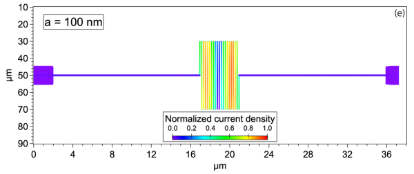
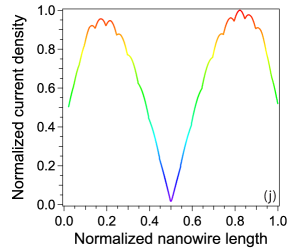
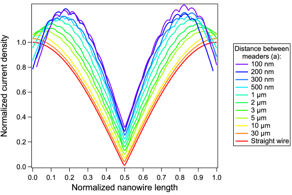
In this section, we analyze the influence of meandering the nanowire to qualitatively study the role of any geometry dependent parasitic capacitance. For that purpose, we simulate the frequency response and current density of various nanowire superinductors using Sonnet em microwave simulator. In order to reduce meshing and simulation times, we simulate -wide nanowires in a simple step-impedance resonator geometry. We start by simulating a straight nanowire as a reference and then proceed to simulate nanowires in a meandered geometry with a fixed meander length while gradually decreasing distance between meanders from (typical distance in our devices) to (see figure S3).
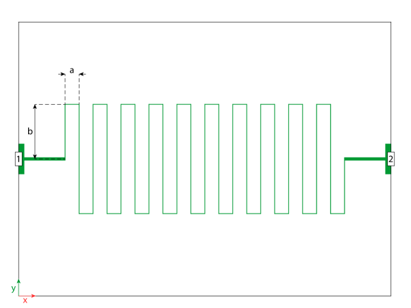
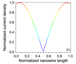
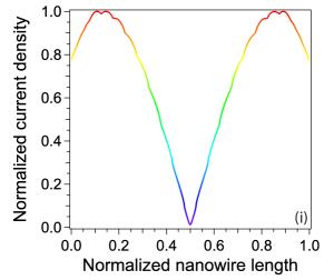
Figures S4 and S5 show the normalized current density along the nanowires at the fundamental resonance frequency of the simulated structure. To be clear, for meandered geometries, the current density is not measured as a line cut along the x-axis, but instead the geometry is unwound and the current density is extracted at every point along the nanowire. We observe that for the straight wire and for , the current density is consistent with the expected mode structure of such a resonator and the characteristic impedance of the nanowire superinductor is well-defined to as described in the main text.
However, below , we observe that, as the distance reduces between the meanders, the resonance frequency significantly diverges from the straight nanowire reference value and the current density is severely distorted. This is explained by the increasing influence of parasitic capacitance between each meander. This parasitic capacitance is equivalent to shunting the nanowire with an extra capacitance and lowering its impedance. Moreover, the structure cannot be treated as a resonator anymore and has therefore no well-defined wave impedance.
References
- Chen et al. (2006) Y. Chen, H. Yang, and Z. Cui, Microelect. Eng. 83, 1119 (2006).
- Peltonen et al. (2013) J. T. Peltonen, O. V. Astafiev, Y. P. Korneeva, B. M. Voronov, A. A. Korneev, I. M. Charaev, A. V. Semenov, G. N. Golt’sman, L. B. Ioffe, T. M. Klapwijk, and J. S. Tsai, Phys. Rev. B 88, 220506 (2013).
- Gao et al. (2008) J. Gao, M. Daal, A. Vayonakis, S. Kumar, J. Zmuidzinas, B. Sadoulet, B. A. Mazin, P. K. Day, and H. G. Leduc, Appl. Phys. Lett. 92, 152505 (2008).
- Lindström et al. (2009) T. Lindström, J. E. Healey, M. S. Colclough, C. M. Muirhead, and A. Y. Tzalenchuk, Phys. Rev. B 80, 132501 (2009).
- Pound (1946) R. V. Pound, Rev. Sci. Instrum. 17, 490 (1946).
- Black (2001) E. D. Black, Am. J. Phys. 69, 79 (2001).
- Lindström et al. (2011) T. Lindström, J. Burnett, M. Oxborrow, and A. Y. Tzalenchuk, Rev. Sci. Instrum. 82, 104706 (2011).
- de Graaf et al. (2012) S. E. de Graaf, A. V. Danilov, A. Adamyan, T. Bauch, and S. E. Kubatkin, J. Appl. Phys. 112, 123905 (2012).
- de Graaf et al. (2017) S. E. de Graaf, A. A. Adamyan, T. Lindström, D. Erts, S. E. Kubatkin, A. Y. Tzalenchuk, and A. V. Danilov, Phys. Rev. Lett. 118, 057703 (2017).