Moiré structure of MoS2 on Au(111): Local structural and electronic properties
Abstract
Monolayer islands of molybdenum disulfide (MoS2) on Au(111) form a characteristic moiré structure, leading to locally different stacking sequences at the S–Mo–S–Au interface. Using low-temperature scanning tunneling microscopy (STM) and atomic force microscopy (AFM), we find that the moiré islands exhibit a unique orientation with respect to the Au crystal structure. This indicates a clear preference of MoS2 growth in a regular stacking fashion. We further probe the influence of the local atomic structure on the electronic properties. Differential conductance spectra show pronounced features of the valence band and conduction band, some of which undergo significant shifts depending on the local atomic structure. We also determine the tunneling decay constant as a function of the bias voltage by a height-modulated spectroscopy method. This allows for an increased sensitivity of states with non-negligible parallel momentum and the identification of the origin of the states from different areas in the Brillouin zone.
I Introduction
Transition metal dichalcogenides are a very interesting class of material with quasi-two-dimensional properties due to their van der Waals-layered structure. Molybdenum disulfide (MoS2), which is a semiconductor when grown in the 2H-structure, belongs to this class of materials, with each sheet consisting of a Mo atomic layer sandwiched between two S planes as shown in figure 1a. Whereas the bulk crystal exhibits an indirect band gap, a single layer has a direct band gap located at the point of the Brillouin zone (BZ) Mak ; Splendiani . The optical gap amounts to Mak ; Splendiani , which covers the energy range of the visible spectrum and renders it interesting for optoelectronic devices. The electronic band gap is larger by the exciton binding energy Tawinan ; Ashwin ; Komsa ; Qiu ; Ugeda .
Single-layer (SL) MoS2 can be obtained by exfoliation methods or by growing it directly on a variety of surfaces, providing large islands of high quality Gronborg ; Sorensen ; Shi ; Lee ; Zhan ; Wang . When the MoS2 layer is in contact with a metal surface, the band structure is strongly modified, due to screening Roesner and hybridization effects Sorensen ; Bruix ; Dedzik . Bruix et al. have shown that the hybridization with a Au surface most strongly affects the states at the point due to their out-of-plane character. In contrast, the states at the point remain largely unperturbed. This can be explained by their in-plane character Bruix and the fact that the point of MoS2 lies in a projected bulk band gap of the Au substrate Miwa ; Cabo .
On Au(111) the monolayer MoS2 islands exhibit a lattice mismatch with the underlying surface and, thus, form a moiré superstructure Bruix ; Sorensen . One may expect that the local variations in atomic structure at the interface may lead to different strengths in the hybridization and screening effects. The moiré structure would thus not only show topographic height variations but also periodic changes in the electronic structure. Local measurement techniques, such as scanning tunneling microscopy and spectroscopy (STM/STS) are ideally suited to study the interplay of atomic-scale structure and electronic properties. However, the drawback of STM is the lack of -space resolution. This challenge has recently been partially overcome by a measurement technique introduced by Zhang et al. Zhang . Detecting the bias-dependent lock-in signal from an oscillating tip allows to extract the tunneling decay constant, which entails information on the parallel momentum of the tunneling electron.
After characterizing the stacking of the MoS2 layer in detail, we use this technique to study the local electronic properties of MoS2 on Au(111). We show which states are affected by the different local interface structure with Au, and which states remain rather unaffected.
II Experimental details
The Au(111) substrate was cleaned by repeated sputtering and annealing cycles under ultrahigh vacuum conditions. For the growth of monolayer MoS2 islands, we adapted a recipe from Grønborg et al Gronborg . Molybdenum was deposited for in an H2S atmosphere of onto the clean Au(111) surface by electron-beam evaporation from a high-purity rod. To obtain MoS2 islands covering less than half of the Au(111) substrate, different evaporation rates of Mo were used, all below onlayer per hour. Subsequently, the sample was annealed for 30 min at in H2S atmosphere. Afterwards, the sample was transferred without exposing it to air into a CreaTec scanning tunneling microscope (STM) with a base temperature of . The microscope is equipped with a qPlus tuning fork sensor for combined measurements of tunneling and atomic force microscopy Giessibl . Scanning tunneling spectroscopy (STS) was performed using a lock-in amplifier (, ). The STM tip was formed by controlled indentation into the surface and its quality assured by reference STS on the bare Au(111) surface.
In order to assess our results of the MoS2 electronic structure, we performed simple band structure calculations with the Quantum Espresso 6.0 package QE of freestanding single layer MoS2. Valence electrons were described by plane wave basis sets with kinetic energy cut off and the Projector Augmented Waves (PAW) method with the PBE approximation to the exchange-correlation functional were used. Our results are consistent with other SL-MoS2 band structures from the literature Bruix ; Qiu ; Padilha .
III Single-layer MoS2 islands on Au(111)
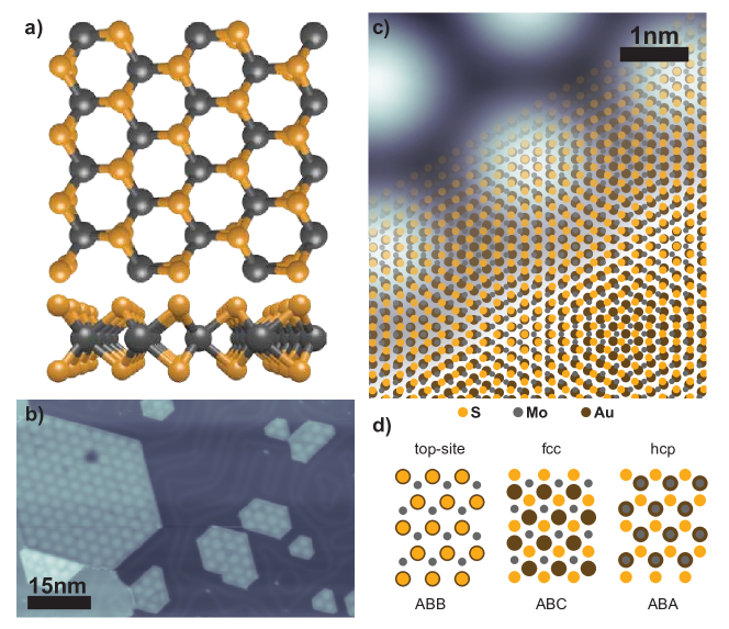
The above described growth procedure leads to single-layer MoS2 islands on Au(111) (Fig. 1b). The herringbone reconstruction of the Au(111) surface is lifted by the MoS2 islands, leading to the irregular orientation of the soliton lines around the MoS2 islands Gronborg . The islands appear with a characteristic hexagonal moiré pattern with a periodicity of about 3.3 nm Bruix ; Sorensen . This structure occurs due to the lattice mismatch of the Au substrate and the MoS2 layer, as depicted in Fig. 1c. As a result the moiré unit cell contains three domains with different stacking of MoS2 and the top Au layer: one top-site and two hollow-site alignments (Fig. 1c,d). Omitting the upper S layer, we label the lattice site of the Mo layer with ”A” and the lattice site of the bottom S layer with ”B”, whereas the lattice site of the upper Au layer depends on the stacking domain. When the bottom layer S atoms are on top of Au atoms, the layer stacking can be referred to as ABB, since S and Au have the same lattice site. In the fcc-like hollow-site stacking of the bottom S layer, the Mo atom is also in a hollow-site, thus yielding an ABC stacking. In the hcp-like hollow-site stacking of S, the Mo atoms are above the top-layer Au atoms, leading to an overall ABA stack.
IV Characterization of stacking sequence of MoS2 layers on Au(111)
The moiré structure found in STM images is an expression of the periodically modulated topographic height convoluted with variations in the electronic structure. To disentangle topographic and electronic effects, we performed atomic force microscopy (AFM) measurements. A constant-height frequency-shift image is shown in Fig. 2a, measured in the attractive force regime. In this measurement mode, the top-layer sulfur atoms appear as depressions in the frequency shift. The two different hollow sites are labelled and in the following, since we cannot assign a stacking order yet. The signal along the two hollow sites is marked in the image and displayed in Fig. 2b as dashed green line. For better visibility a smoothed contour was added in black. The linear offset in the graph is due to a slight angle in the constant-height plane. Taking this linear offset into account, hollow-site provides about less frequency shift than compared to hollow-site and is thereby topographically lower.
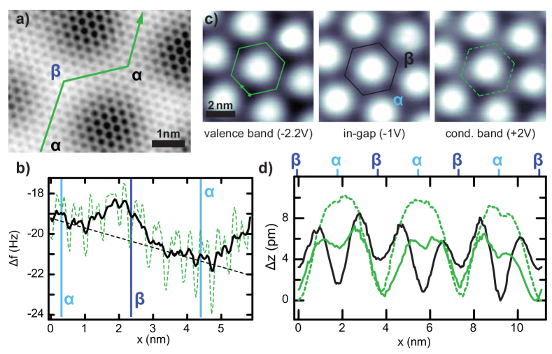
In the STM the situation appears reversed, when measuring at energies in the band gap of MoS2, which is on Au(111) between Miwa and Cabo . Figure 2c shows the topography of MoS2 when measured with STM at energies of the valence band (left), conduction band (right) and in the band gap (middle). The apparent topographic heights measured along a closed path marked in figure 2c are displayed in figure 2d. When measured within the band gap, hollow-site appears higher than , even though it is topographically lower, as shown by AFM. At higher energies outside of the band gap, hollow-site appears higher again.
Comparing the STM and AFM results yields information about the hybridization of MoS2 with the Au surface. Small deviations in the distance between MoS2 and substrate, lead to a stronger or weaker hybridization and, thus, changes the in-gap STM signal. Even though hollow-site is closer to the surface, the stronger hybridization provides a larger tunneling current, causing it to appear higher in STM. In the extreme case of a missing Au layer under a small area of MoS2 – due to a vacancy island of a few nanometers – that area already appears completely transparent for the STM Pits .
In order to assign the two different hollow sites to a certain stacking sequence, the orientation of the MoS2 islands have to be known. Small islands of MoS2 on Au(111) often appear as triangles or truncated triangles, where the longer edges are assumed to be the so-called Mo-edges Bollinger ; Nielsen as depicted in Fig. 3a. Following this assumption, the lattice orientation of the MoS2 islands can be determined and compared to the orientation of the different hollow-sites. Thereby, the hollow-site would correspond to the ABC stacking and to the ABA stacking sequence as is sketched in Fig. 1d.
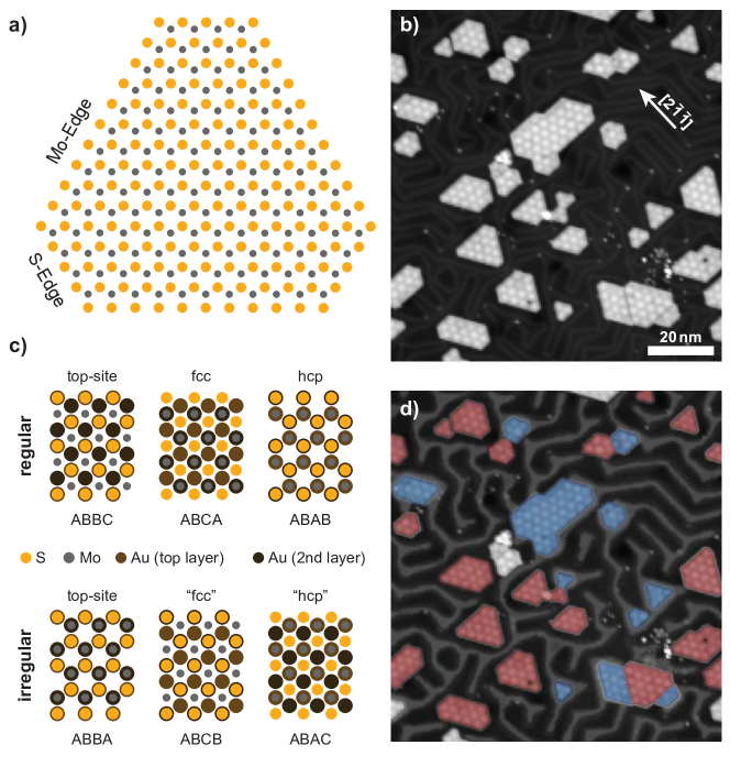
For a complete characterization of the adsorption structure on the Au(111) surface, also the second layer of the Au(111) crystal has to be taken into account. With respect to the first two layers of Au, there are two orientations in which a MoS2 island can grow. These are sketched in Fig. 3c and labeled as regular and irregular stacking. In the ”regular” orientation all four layers of the Mo-S-Au-Au interface are stacked in a normal fcc or hcp fashion at the two hollow sites, which can be associated to an ABCA and ABAB stacking, respectively. In contrast, the ”irregular” orientation leads to a mixed stacking with ABCB and ABAC sequence, which is not fully compliant with the fcc or hcp nomenclature.
If there is a preferred stacking of MoS2 on the Au(111) crystal, it will be observable in the ratio of the two different orientations. An overview of MoS2 islands on Au(111) is displayed in Fig. 3b and in Fig 3d, where their orientations are marked by red or blue color. The orientation of larger islands without triangular shape was determined by the orientations of their hollow sites (see Fig. 2c). Since the first two layers of the Au(111) surface are of interest, the surface reconstruction has to be taken into account here. This herringbone structure is a reconstruction, where the upper layer of the Au(111) surface alternates between fcc and hcp stacking Hove ; Barth . By fitting a hexagonal grid to an image with atomic resolution of the herringbone reconstruction, the orientation of the Au crystal was determined and is depicted in Fig. 3b. The hcp domains of the Au(111) surface are marked in light grey in Fig. 3d.
The MoS2 islands in Fig. 3d with orientation marked red, are all lying on the fcc domain of the herringbone reconstruction. In contrast, the blue marked islands, which provide a reversed orientation, are all located in the hcp domain. This behaviour can also be seen in the STM images of other published data Nielsen ; Lauritsen . Thus, both orientations provide the same stacking of the Mo-S-Au-Au interface, indicating there is an energetically favourable stacking of MoS2 on Au(111). Assuming again the long edges to be Mo-edges, the preferred orientation is the regular stacking as depicted in Fig. 3c.
Summarizing this part, we have shown that the MoS2 islands all exhibit the very same orientation and overall the same atomic interface structure with respect to the Au(111) surface. We were also able to assign the two hollow sites and to the fcc and hcp stacking order, respectively. With the moiré structure providing differences in the local atomic structure, we now turn to the question, whether the electronic structure is affected by the different atomic configurations in the top sites and hollow sites.
V Electronic structure of MoS2 on Au(111)
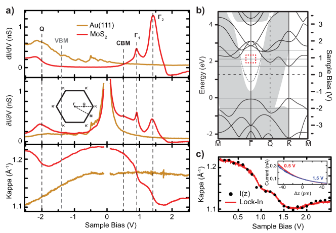
In order to resolve the local electronic structure of MoS2 we first employ the most common spectroscopic mode of STM. This method consists of recording constant-height d/d spectra as depicted in the uppermost graph of Fig. 4a. The spectrum was taken at the top-site configuration of the moiré pattern and shows three prominent features. There is a shoulder at a bias voltage of , and there are two peaks at and . Neither of the three features matches the expected energies from ARPES measurements of the valence band maximum (VBM) at Miwa or conduction band minimum (CBM) at Cabo , marked by vertical dashed lines. Since they are located at the point of the BZ (see Fig. 4b), they are not easily detectable in a d/d spectrum. This can be explained by STS being mainly sensitive to states with small in-plane momentum around the point. The tunneling current is strongly distance dependent, with an exponential decay Tersoff1983 ; Tersoff1985 . The decay constant depends on the energy barrier for tunneling , as well as on of the probed state. Thus, states with a large component – e.g. the VBM and CBM at the edge of the BZ – have a large decay constant and therefore do not contribute significantly to the total tunneling current at large tip-sample distances. Hence, it is not surprising to not find signatures of the VBM and CBM in the d/d spectrum.
In constant-current / spectra the tunneling barrier height is adjusted by a feedback loop, which regulates the current to a constant value. A spectrum recorded in this mode is shown in Fig. 4a in the middle panel. The tip-height adjustment enhances the sensitivity to states with larger component at energies smaller than the band gap at . With this method, we detect a small feature at , which agrees with the expected value for the CBM from ARPES measurements Cabo .
Recently, Zhang et al. reported an STS-based method using the enhanced sensitivity of / spectra, in order to measure the of states and, thus, determine their position in the BZ. By modulating the tip height , they were able to measure the d/d signal with a lock-in amplifier, as long as the modulation is faster than the constant-current feedback. The decay constant is then determined by , where is the set-point current.
We adapted this method by measuring the / and d/d signal simultaneously. For the d/d measurement the tip was oscillated with at an amplitude of . Control measurements showed no significant crosstalk between the / and d/d signals. In order to calibrate the lock-in d/d signal, we also recorded spectra at different bias voltages. These I(z) curves were fitted by (see inset in Fig. 4c). The extracted values were used to rescale the lock-in signal of the d/d measurement.
The rescaled d/d spectrum for MoS2 on Au(111) is displayed in the bottom panel of Fig. 4a. The reference spectrum, taken on the Au(111) surface, shows a nearly constant value of at positive bias voltages. As sketched in the background of Fig. 4b, Au provides a projected bulk band gap at around and above . This hosts a Shockley surface state, which dominates in the tunneling current. Due to the parabolic dispersion of the surface state, the corresponding value increases with energy, shifting to higher values. In contrast, a larger bias voltage lowers the energy barrier for tunneling , with being the energy barrier without applied bias. These two effects cancel each other and lead to a nearly constant .
At negative bias voltages below , Au exhibits occupied bands around . Consequently, the main contribution to the tunneling current originates from tunneling out of these states, leading to a decrease of . Please note, the measured value is the averaged decay constant of the whole tunnel current, not of single states. Hence, the signal increases or decreases with the bias voltage when tunneling into a state, with the steepest slope of at the maximum in the / spectrum. For a good estimation of the bias voltage should be larger than the corresponding state, in order to have the highest contribution of tunneling current into that state.
At small bias voltages the decay constant measured on MoS2 is , which is considerably larger than on Au. This indicates that the MoS2 layer does not exhibit states at in this energy range and a higher energy barrier of the tunneling process than Au(111). The latter agrees with the observation of an -doped MoS2 layer on Au(111) Bruix .
With increasing bias voltage, decreases on MoS2. A pronounced drop of occurs at and , indicating that tunneling at these bias voltages is accompanied by a drastic change in the component. This evidences the onset of tunneling into states at different parts of the BZ and suggests that the tunneling spectra may be used for identifying characteristic points in the BZ. In particular, the drop of of MoS2 below the value measured on Au(111) at shows that MoS2 states are located in the projected bulk band gap of Au.
To identify the relevant bands in the tunneling spectra, we now compare the location of the sudden change in with band-structure calculations of free-standing MoS2 (Fig. 4b). They reflect the direct band gap at and an increased band gap at . The onset of unoccupied bands lies at approximately at . We suggest to associate these band onsets with the peak at in the d/d spectra. This assignment is corroborated by the drop in , which is in agreement with tunneling into bands at . In the following, this state will be labeled as . At bias voltages larger than the decay constant increases again, in agreement with the band structure calculations, where the parallel momentum of the bands increases again.
Assuming the current at is dominated by tunneling into , i.e., , a rough estimation would be that . By comparing with the of a different state, the parallel momentum of this state can be estimated using .
Depending on whether the total decay constant is increasing or decreasing by tunneling into the state, this estimation yields a lower or a upper boundary value, respectively. Applied to the state at , it results in a parallel momentum of , whereas the point is located at Boker . According to these results, there has to be a state located at the point approximately above the CBM, marked by a red box in figure 4b. This state will be labeled as in the following and may originate from hybridization of Au and MoS2 states or from the formation of an interface state. Please note, that other calculations in literature, which include the underlying Au substrate, do not predict a MoS2 state above the CBM either Bruix .
At negative bias voltage the decay constant of MoS2 first decreases in a similar fashion as the one of Au, indicating that the current in this regime is dominated by tunneling into the Au states. We observe a state in the / spectra at , which is accompanied by an increase of up to . Since the largest part of the tunneling at happens from this state, we can estimate its parallel momentum with . This corresponds to a location at in the BZ. Accordingly, the state will be referred to as in the following. For free-standing MoS2 a band at would have been expected at energies close to the VBM and crossing at energies further away from the Fermi level (see figure 4b). However our measurements do not indicate any state at . This observation is in agreement with ARPES results Miwa and has been explained by hybridization of the MoS2 states with the -band continuum states of Au Bruix . We note that we cannot identify the VBM, which we assign to the presence of the hybridized states at the same energy around , which dominate the tunneling current.
VI Influence of the moiré pattern on the local spectra
Our previous results evidence the different contributions of states at different points in the BZ to the tunneling current. Admittedly, this is not the simplest and most obvious way for determining the electronic band structure of a surface. However, STM provides unprecedented spatial resolution of the electronic properties. Hence, we investigate now the influence of atomic-scale structural changes on the local electronic properties.
In Fig. 5a the tunneling spectra for the three different regions of the moiré superstructure are displayed. The two different hollow sites are labeled fcc and hcp, according to the findings above. The most pronounced difference in the spectra is that the state is shifted by towards for both hollow sites compared to the spectrum taken at top site. This shift could be caused by a stronger hybridization of the MoS2 with the Au substrate or due to a more effective electronic screening Roesner . The unoccupied state is slightly shifted away from by .
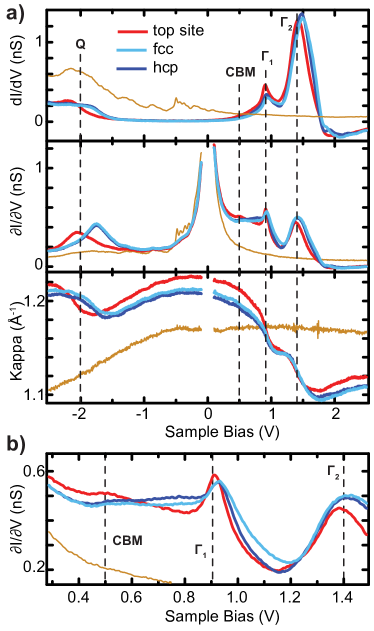
In the / spectrum a distinction between all three sites can be observed around (Zoom shown in Fig. 5b). In the energy range between the CBM and the signal of the top site differs from the two hollow-sites, whereas between and the fcc hollow site differs from the other two spectra. Except for a low-intensity signal at , all other features are nearly identical for the two hollow sites. Thus, surprisingly, the state seems to be affected by the stacking order in the hollow sites. This observation supports the assumption that the state at occurs due to interactions of MoS2 with the Au(111) substrate. It is also in agreement with the absence of such a state when the MoS2 is placed on other materials with weaker interaction like graphene Zhang .
Calculations of MoS2 on Au(111) from literature Bruix predict a rigid shift of between top site and hollow sites, whereas we observe an unequal shift of and . Aside from that difference, the details of the spectra agree, i.e. the shift of the low-intensity signal at and the variation of between the two hollow sites agree with the predictions from Ref. Bruix . The latter can also be seen in STS taken at room temperature Sorensen .
The tunneling decay constant is not significantly affected by the differences between the hollow sites. The spectra only reveal a difference between the hollow and top site with a reduced barrier by within the band gap at the hollow sites. This effect could be due to the reduced distance between MoS2 and Au(111), causing a smaller dipole moment at the interface.
VII Conclusions
The electronic properties of MoS2 on Au(111) deviate significantly from those of their free-standing analogues. ARPES combined with theoretical calculations had already provided an in-depth analysis of the hybridization effects at the valence band Bruix ; Miwa . Our work adds information on the local scale to these earlier studies. Using STM and AFM experiments, we are able to identify the precise stacking structure of the moiré pattern on the two topmost layers of Au(111). This result does not only provide a model of the atomic structure at the MoS2/Au(111) interface, it also evidences a unique growth mode. We show that all MoS2 islands have a certain orientation on the substrate, depending on the stacking of the two top Au layers. Assuming the so called Mo-edges to be the preferred termination of the islands, the exact stacking of MoS2 on Au(111) could be determined. Recently, Bana et al. achieved the growth of a large, single-orientation MoS2 monolayer on Au(111) Bana . We speculate that the growth of such a single-orientation layer is driven by the unique stacking sequence, which we also find in the smaller islands.
Using a recently proposed method of tunneling spectroscopy and extracting the voltage-dependent tunneling decay constant of the hybrid MoS2/Au(111) structure, we show that there is a state of MoS2 located at the point around . This state is absent in free-standing MoS2 and can be ascribed to hybridization with the underlying substrate. We also show that this state is sensitive to the local atomic stacking configuration of the MoS2 layer on Au(111).
Our results reveal that atomic-scale changes at a MoS2 interface may significantly influence the electronic structure. This puts stringent requirements of clean interface or a precise knowledge of defects on the design of MoS2-based devices.
VIII Acknowledgments
We gratefully acknowledge funding by the Deutsche Forschungsgemeinschaft through Sfb 658 and TRR 227.
References
- (1) K. F. Mak, C. Lee, J. Hone, J. Shan, T. F. Heinz, Atomically thin MoS2: A new direct-gap semiconductor, Phys. Rev. Lett. 105 (13) (2010) 136805. doi:10.1103/PhysRevLett.105.136805.
- (2) A. Splendiani, L. Sun, Y. Zhang, T. Li, J. Kim, C. Chim, G. Galli, F. Wang, Emerging photoluminescence in monolayer MoS2, Nano Lett. 10 (4) (2010) 1271. doi:10.1021/nl903868w.
- (3) T. Cheiwchanchamnangij, W. R. L. Lambrecht, Quasiparticle band structure calculation of monolayer, bilayer, and bulk MoS2, Phys. Rev. B 85 (20) (2012) 205302. doi:doi.org/10.1103/PhysRevB.85.205302.
- (4) A. Ramasubramaniam, Large excitonic effects in monolayers of molybdenum and tungsten dichalcogenides, Phys. Rev. B 86 (11) (2012) 115409. doi:10.1103/PhysRevB.86.115409.
- (5) H. Komsa, A. V. Krasheninnikov, Effects of confinement and environment on the electronic structure and exciton binding energy of MoS2 from first principles, Phys. Rev. B 86 (24) (2012) 241201. doi:10.1103/PhysRevB.86.241201.
- (6) D. Y. Qiu, F. H. da Jornada, S. G. Louie, Optical spectrum of MoS2: Many-body effects and diversity of exciton states, Phys. Rev. Lett. 111 (21) (2015) 216805. doi:10.1103/PhysRevLett.111.216805.
- (7) M. Ugeda, A. J. Bradley, S. Shi, F. H. da Jornada, Y. Zhang, D. Qiu, W. Ruan, S. Mo, Z. Hussain, Z. Shen, F. Wang, S. Louie, M. F. Crommie, Giant bandgap renormalization and excitonic effects in a monolayer transition metal dichalcogenide semiconductor, Nature Materials 13 (2014) 1091. doi:1038/nmat4061.
- (8) S. S. Grønborg, S. Ulstrup, M. Bianchi, M. Dendzik, C. E. Sanders, J. V. Lauritsen, P. Hofmann, J. A. Miwa, Synthesis of epitaxial single-layer MoS2 on Au(111), Langmuir 31 (35) (2015) 9700. doi:10.1021/acs.langmuir.5b02533.
- (9) S. G. Sørensen, H. G. Füchtbauer, A. K. Tuxen, A. S. Walton, J. V. Lauritsen, Structure and electronic properties of in situ synthesized single-layer MoS2 on a gold surface, ACS Nano 8 (7) (2014) 6788. doi:10.1021/nn502812n.
- (10) Y. Shi, W. Zhoi, A. Lu, W. Fank, Y. Lee, A. L. Hsu, S. M. Kim, K. K. Kim, H. Y. Yang, L. Li, J. Idrobo, J. Kong, van der Waals epitaxy of MoS2 layers using graphene as growth templates, Nano Lett. 12 (6) (2012) 2784. doi:10.1021/nl204562j.
- (11) Y. Lee, X. Zhang, W. Zhang, M. Chang, C. Lin, K. Chang, Y. Yu, J. T. Wang, C. Chang, L. Li, T. Lin, Synthesis of large-area MoS2 atomic layers with chemical vapor deposition, Adv. Mater. 24 (17) (2012) 2320. doi:10.1002/adma.201104798.
- (12) Y. Zhan, Z. Liu, S. Najmaei, P. M. Ajayan, J. Lou, Large-area vapor-phase growth and characterization of MoS2 atomic layers on a SiO2 substrate, small 8 (7) (2012) 966. doi:10.1002/smll.201102654.
- (13) S. Wang, X. Wang, J. H. Warner, All chemical vapor deposition growth of MoS2:h-bn vertical van der Waals heterostructures, ACS Nano 9 (5) (2015) 5246. doi:0.1021/acsnano.5b00655.
- (14) M. Rösner, C. Steinke, M. Lorke, C. Gies, F. Jahnke, T. O. Wehling, Two-dimensional heterojunctions from nonlocal manipulations of the interactions, Nano Lett. 16 (4) (2016) 2322. doi:10.1021/acs.nanolett.5b05009.
- (15) A. Bruix, J. A. Miwa, N. Hauptmann, D. Wegner, S. Ulstrup, S. S. Grønborg, C. E. Sanders, M. Dendzik, A. Grubiić abo, M. Bianchi, J. V. Lauritsen, A. A. Khajetoorians, B. Hammer, P. Hofmann, Single-layer MoS2 on Au(111): Band gap renormalization and substrate interaction, Phys. Rev. B 93 (16) (2016) 165422. doi:10.1103/PhysRevB.93.165422.
- (16) M. Dedzik, A. Bruix, M. Michiardi, A. S. Ngankeu, M. Bianchi, J. A. Miwa, B. Hammer, P. Hofmann, C. E. Sanders, Substrate-induced semiconductor-to-metal transition in monolayer WS2, Phys. Rev. B 96 (23) (2017) 235440. doi:10.1103/PhysRevB.96.235440.
- (17) J. Miwa, S. Ulstrup, S. G. Sørensen, M. Dendzik, A. Grubiić abo, M. Bianchi, J. V. Lauritsen, P. Hofmann, Electronic structure of epitaxial single-layer MoS2, Phys. Rev. Lett. 114 (4) (2014) 046802. doi:10.1103/PhysRevLett.114.046802.
- (18) A. Grubiić abo, J. A. Miwa, S. S. Grønborg, J. M. Riley, J. C. Johannsen, C. Cacho, O. Alexander, R. T. Chapman, E. Springate, M. Grioni, J. V. Lauritsen, P. D. C. King, P. Hofmann, S. Ulstrup, Observation of ultrafast free carrier dynamics in single layer MoS2, Nano Lett. 15 (9) (2015) 5883. doi:10.1021/acs.nanolett.5b01967.
- (19) C. Zhang, Y. Chen, A. Johnson, M. Li, L. Li, P. C. Mende, R. M. Feenstra, C. Shih, Probing critical point energies of transition metal dichalcogenides: Surprising indirect gap of single layer WSe2, Nano Lett. 15 (10) (2015) 6494. doi:10.1021/acs.nanolett.5b01968.
- (20) F. Giessibl, Atomic resolution on Si(111)-(7x7) by noncontact atomic force microscopy with a force sensor based on a quartz tuning fork, Appl. Phys. Lett 76 (11) (2000) 1470. doi:10.1063/1.126067.
- (21) P. t. Giannozzi, Quantum espresso: a modular and open-source software project for quantum simulations of materials, J. Phys. Condens. Matter 21 (39) (2009) 395502. doi:10.1088/0953-8984/21/39/395502.
- (22) J. E. Padilha, H. Peelaers, A. Janotti, C. G. Van de Walle, Nature and evolution of the band-edge states in MoS2: From monolayer to bulk, Phys. Rev. B 90 (20) (2014) 205420. doi:10.1103/PhysRevB.90.205420.
- (23) N. Krane, C. Lotze, J. Läger, G. Reecht, K. J. Franke, Electronic structure and luminescence of quasi-freestanding MoS2 nanopatches on Au(111), Nano Lett. 16 (8) (2016) 5163. doi:10.1021/acs.nanolett.6b02101.
- (24) M. V. Bollinger, J. V. Lauritsen, K. W. Jacobsen, J. K. Nørskov, S. Helveg, F. Besenbacher, One-dimensional metallic edge states in MoS2, Phys. Rev. Lett. 87 (19) (2001) 196803. doi:10.1103/PhysRevLett.87.196803.
- (25) J. H. Nielsen, L. Bech, K. Nielsen, Y. Tison, K. P. Jørgensen, J. L. Bonde, S. Horch, T. F. Jaramillo, I. Chrokendorff, Combined spectroscopy and microscopy of supported MoS2 nanoparticles, Surface Science 603 (9) (2009) 1182. doi:10.1016/j.susc.2009.02.039.
- (26) M. A. Van Hove, R. J. Koestner, P. C. Stair, J. P. Bibérian, L. L. Kesmodel, I. Barto, G. A. Somorjai, The surface reconstructions of the (100) crystal faces of iridium, platinum and gold: I. experimental observations and possible structural models, Surface Science 103 (1) (1981) 189. doi:10.1016/0039-6028(81)90107-2.
- (27) J. V. Barth, H. Brune, G. Ertl, R. J. Behm, Scanning tunneling microscopy observations on the reconstructed Au(111) surface: Atomic structure, long-range superstructure, rotational domains, and surface defects, Phys. Rev. B 42 (15) (1990) 9307. doi:10.1103/PhysRevB.42.9307.
- (28) J. V. Lauritsen, J. Kibsgaard, G. H. Olesen, P. G. Moses, B. Hinnemann, S. Helveg, J. K. Nørskovb, B. S. Clausenc, H. Topsøe, E. Læsgaard, Location and coordination of promoter atoms in Co- and Ni-promoted MoS2-based hydrotreating catalysts, Journal of Catalysis 249 (2) (2007) 220. doi:10.1016/j.jcat.2007.04.013.
- (29) N. Takeuchi, C. T. Chan, K. M. Ho, Au(111): A theoretical study of the surface reconstruction and the surface electronic structure, Phys. Rev. B 43 (17) (1991) 13899. doi:10.1103/PhysRevB.43.13899.
- (30) J. Tersoff, D. R. Hamann, Theory and application for the scanning tunneling microscope, Phys. Rev. Lett. 50 (25) (1983) 1998. doi:10.1103/PhysRevLett.50.1998.
- (31) J. Tersoff, D. R. Hamann, Theory of the scanning tunneling microscope, Phys. Rev. B 31 (2) (1985) 805. doi:10.1103/PhysRevB.31.805.
- (32) T. Böker, A. Severin, A. Müller, C. Janowitz, R. Manzke, D. Voß, P. Krüger, A. Mazur, J. Pollman, Band structure of MoS2, MoSe2, and -MoTe2: Angle-resolved photoelectron spectroscopy and ab initio calculations, Phys. Rev. B 64 (23) (2001) 235305. doi:10.1103/PhysRevB.64.235305.
- (33) H. Bana, E. Travaglia, L. Bignardi, P. Lacovig, C. E. Sanders, M. Dendzik, M. Michiardi, M. Bianchi, d. Lizzit, F. Presel, D. De Angelis, N. Apostol, P. Kumar Das, J. Fujii, I. Vobornik, R. Larciprete, A. Baraldi, P. Hofmann, S. Lizzit, Epitaxial growth of single-orientation high-quality MoS2 monolayers, arXiv:1802.02220.