Approaching perfect absorption of monolayer molybdenum disulfide at visible wavelengths using critical coupling
Xiaoyun Jiang, Tao Wang,* Shuyuan Xiao, Xicheng Yan, Le Cheng, and Qingfang Zhong
Wuhan National Laboratory for Optoelectronics, Huazhong University of Science and Technology, Wuhan 430074, China
*wangtao@hust.edu.cn
Abstract
A simple perfect absorption structure is proposed to achieve the high efficiency light absorption of monolayer molybdenum disulfide (MoS2) by the critical coupling mechanism of guided resonances. The results of numerical simulation and theoretical analysis show that the light absorption in this atomically thin layer can be as high as at the visible wavelengths, which is over times more than that of a bare monolayer MoS2. In addition, the operating wavelength can be tuned flexibly by adjusting the radius of the air hole and the thickness of the dielectric layers, which is of great practical significance to improve the efficiency and selectivity of the absorption in monolayer MoS2. The novel idea of using critical coupling to enhance the light-MoS2 interaction can be also adopted in other atomically thin materials. And the meaningful improvement and tunability of the absorption in monolayer MoS2 provide a good prospect for the realization of high-performance MoS2-based optoelectronic applications, such as photodetection and photoluminescence.
OCIS codes: (310.6860) Thin films, optical properties; (300.1030) Absorption; (050.6624) Subwavelength structures.
References and links
- [1] F. Bonaccorso, Z. Sun, T. Hasan, and A. C. Ferrari, “Graphene photonics and optoelectronics,” Nat. Photonics 4(9), 611–622 (2010).
- [2] Q. H. Wang, K. Kalantar-Zadeh, A. Kis, J. N. Coleman, and M. S. Strano, “Electronics and optoelectronics of two-dimensional transition metal dichalcogenides,” Nat. Nanotechnol. 7(11), 699–712 (2012).
- [3] X. He, P. Gao, and W. Shi, “A further comparison of graphene and thin metal layers for plasmonics,” Nanoscale 8, 10388–10397 (2016).
- [4] J. Zhang, Z. Zhu, W. Liu, X. Yuan, and S. Qin, “Towards photodetection with high efficiency and tunable spectral selectivity: graphene plasmonics for light trapping and absorption engineering,” Nanoscale 7(32), 13530–13536 (2015).
- [5] S. Xiao, T. Wang, Y. Liu, C. Xu, X. Han, and X. Yan,“Tunable light trapping and absorption enhancement with graphene ring arrays,” Phys. Chem. Chem. Phys. 18(38), 26661–26669 (2016).
- [6] X. Yan, T. Wang, S. Xiao, T. Liu, H. Hou, L. Cheng, and X. Jiang, “Dynamically controllable plasmon induced transparency based on hybrid metal-graphene metamaterials,” Sci. Rep. 7(1), 13917 (2017).
- [7] S. Xiao, T. Wang, T. Liu, X. Yan, Z. Li, and C. Xu, “Active modulation of electromagnetically induced transparency analogue in terahertz hybrid metal-graphene metamaterials,” Carbon 126, 271–278 (2018).
- [8] X. Jiang, T. Wang, S. Xiao, X. Yan, and L. Cheng, “Tunable ultra-high-efficiency light absorption of monolayer graphene using critical coupling with guided resonance,” Opt. Express 25(22), 27028–27036 (2017).
- [9] S. X. Xia, X. Zhai, Y. Huang, J. Q. Liu, L. L. Wang, and S. C. Wen, “Multi-band perfect plasmonic absorptions using rectangular graphene gratings,” Opt. Lett. 42(15), 3052–3055 (2017).
- [10] M. Amin, M. Farhat, and H. Bağcı, “A dynamically reconfigurable Fano metamaterial through graphene tuning for switching and sensing applications,” Sci. Rep. 3, 2105 (2013).
- [11] X. Yan, T. Wang, X. Han, S. Xiao, Y. Zhu, and Y. Wang, “High Sensitivity Nanoplasmonic Sensor Based on Plasmon-Induced Transparency in a Graphene Nanoribbon Waveguide Coupled with Detuned Graphene Square-Nanoring Resonators,” Plasmonics 12(5), 1449–1455 (2017).
- [12] S. Bahauddin, H. Robatjazi, and I. Thomann, “Broadband absorption engineering to enhance light absorption in monolayer MoS2,” ACS Photonics 3(5), 853–862 (2016).
- [13] A. Sobhani, A. Lauchner, S. Najmaei, C. Orozco, F. Wen, J. Lou, and N. Halas, “Enhancing the photocurrent and photoluminescence of single crystal monolayer MoS2 with resonant plasmonic nanoshells,” Appl. Phys. Lett. 104(3), 031112 (2014).
- [14] O. Lopez-Sanchez, D. Lembke, M. Kayci, A. Radenovic, and A. Kis, “Ultrasensitive photodetectors based on monolayer MoS2,” Nat. Nanotechnol. 8(7), 497–501 (2013).
- [15] A. Pospischil, M. M. Furchi, and T. Mueller, “Solar-energy conversion and light emission in an atomic monolayer p-n diode,” Nat. Nanotechnol. 9(4), 257–261 (2014).
- [16] H. Li, M. Qin, L. Wang, X. Zhai, R. Ren, and J. Hu, “Total absorption of light in monolayer transition-metal dichalcogenides by critical coupling,” Opt. Express 25(25), 31612–31621 (2017).
- [17] L. C. Botten, R. C. McPhedran, N. A. Nicorovici, and G. H. Derrick, “Periodic models for thin optimal absorbers of electromagnetic radiation,” Phys. Rev. B 55, R16072 (1997).
- [18] C. Janisch, H. Song, C. Zhou, Z. Lin, A. Elías, D. Ji, M. Terrones, Q. Gan, and Z. Liu, “MoS2 monolayers on nanocavities: enhancement in light-matter interaction,” 2D Mater. 3(2), 025017 (2016).
- [19] H. Lu, X. Gan, D. Mao, Y. Fan, D. Yang, and J. Zhao, “Nearly perfect absorption of light in monolayer molybdenum disulfide supported by multilayer structures,” Opt. Express 25(18), 21630–21636 (2017).
- [20] J. Piper and S. Fan, “Broadband absorption enhancement in solar cells with an atomically thin active layer,” ACS Photonics 3(4), 571–577 (2016).
- [21] Y. Long, H. Deng, H. Xu, L. Shen, W. Guo, C. Liu, W. Huang, W. Peng, L. Li, H. Lin, and C. Guo, “Magnetic coupling metasurface for achieving broad-band and broad-angular absorption in the MoS2 monolayer,” Opt. Mater. Express 7(1), 100–110 (2017).
- [22] S. Butun, S. Tongay, and K. Aydin, “Enhanced light emission from large-area monolayer MoS2 using plasmonic nanodisc arrays,” Nano Lett. 15(4), 2700–2704 (2015).
- [23] C. A. Barrios, V. R. Almeida, R. R. Panepucci, B. S. Schmidt, and M. Lipson, “Compact Silicon Tunable Fabry-Perot Resonator With Low Power Consumption,” IEEE Photonics Technol. Lett. 16(2), 506–508 (2004).
- [24] H. Lu, X. Gan, B. Jia, D. Mao, and J. Zhao, “Tunable high-efficiency light absorption of monolayer graphene via Tamm plasmon polaritons,” Opt. Lett. 41(20), 4743–4746 (2016).
- [25] L. Cheng, T. Wang, X. Jiang, X. Yan, and S. Xiao, “Polarization and angular sensibility in the natural hyperbolic hexagonal boron nitride arrays,” J. Phys. D: Appl. Phys. 50(43), 435104 (2017).
- [26] Y. Li, A. Chernikov, X. Zhang, A. Rigosi, H. Hill, A. Zande, D. Chenet, E. Shih, J. Hone, and T. Heinz, “Measurement of the optical dielectric function of monolayer transition-metal dichalcogenides: MoS2, MoSe2, WS2, and WSe2,” Phys. Rev. B 90(20), 205422 (2014).
- [27] J. Piper and S. Fan, “Total absorption in a graphene monolayer in the optical regime by critical coupling with a photonic crystal guided resonance,” ACS Photonics 1(4), 347–353 (2014).
- [28] D. R. Smith, D. C. Vier, Th. Koschny, and C. M. Soukoulis, “Electromagnetic parameter retrieval from inhomogeneous metamaterials,” Phys. Rev. E 71, 036617 (2005).
- [29] Y. S. Fan, C. C. Guo, Z. H. Zhu, W. Xu, F. Wu, X. D. Yuan, and S. Q. Qin, “Monolayer-graphene-based perfect absorption structures in the near infrared,” Opt. Express 25(12), 13079–13086 (2017).
1 Introduction
Atomically thin two-dimensional (D) materials, such as graphene and monolayer transition metal dichalcogenides (TMDCs), have been intensively studied due to their remarkable mechanical, electrical and optical properties[1, 2, 3]. The unique characteristics of graphene contain the ultra-wide spectral response, the ultra-high carrier mobility and dynamic tunability, which open up many exciting possibilities for nano-integrated optoelectronic devices such as optical detectors[4, 5], modulators[6, 7], metamaterial perfect absorbers (MPA)[8, 9], and biological or chemical sensors[10, 11]. However, pure graphene, though extremely promising, has a fixed zero band gap, which makes it uninteresting from the point of view of the device application. In contrast, TMDCs, a new class of semiconductors with distinctive properties at a single layer thickness, has attracted widespread attention because of its interesting and important optoelectronic characteristics[2]. In particular, molybdenum disulfide (MoS2), representing one of the most special candidates for TMDCs semiconductor applications, has a direct bandgap (around ev) for electronic transition when the bulk structure is converted into monolayer[12]. Owing to its special direct band gap and low dark current, monolayer MoS2 has been considered as the ideal atomically thin D material for photoluminescence[13], photodetection[14], and photovoltaic devices[15, 16]. It is well known that the maximum absorption of a thin absorbing layer under a single illumination in the air cannot exceed [17], and the inherent thickness of the atomically thin layer also hinders the better interaction between light and matter. Therefore, the light absorption in monolayer MoS2 is weak, which seriously restricts the application of MoS2 in the optoelectronics area. For instance, the sing-pass absorption of monolayer MoS2 is only for an atomically thin layer ( nm thickness) in the visible range[18]. So in order to achieve many high-performance MoS2-based optical devices, it is highly desirable to enhance absorption up to . Recently, several approaches have been proposed to improve light absorption in monolayer MoS2[19, 20, 21, 22]. A new multilayer photonic structure was proposed to realize the absolute absorption of light in monolayer MoS2 reached up to in the visible range due to the excitation of highly-confined Tamm plasmon mode[19]. Through the consideration of light trapping theory, the structure of photonic crystal slab as a resonator was designed, in which ideal metallic reflector or dielectric Bragg reflector was considered as a perfect mirror. The optimized design parameters were used to achieve average absorption of over the entire visible spectrum in monolayer MoS2 under normal incidence[20]. The magnetic coupling metasurface has been investigated to boost the light absorption of single MoS2 layer, which could reach within the visible wavelength range [21]. In addition, the strong plasmonic resonances in metallic nanostructures have been widely utilized to boost the light absorption of MoS2[22]. However, up to now, for monolayer MoS2 with atomically thin layer, a much simpler structure with the dynamical wavelength-selective property and ultra-high-efficiency light absorption has yet to be reported.
In this article, we investigate ultra-high-efficiency light absorption in monolayer MoS2 by critical coupling with guided resonance, in the band gap region of MoS2, in which the MoS2 layer is coupled to a D periodic dielectric configuration with low refractive index contrast. Compared with previous research results, we propose a much simpler MPA to effectively enhance the light-matter interaction, resulting in the light absorption of monolayer MoS2 up to . Meanwhile, we are able to control absorption efficiency of MoS2 at different operating wavelengths by adjusting the thickness of dielectric layers and the radius of air hole. In addition, the same principle can be extended to other atomically thin D materials, such as MoSe2, WSe2 and WS2. And we also propose a promising way to enhance the interaction of light with these D materials, which are very important for the application of TMDC-based photodetection and photoluminescence.
2 Structure and model
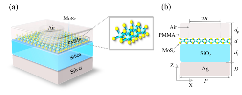
Figure. 1(a) shows the schematic of the proposed monolayer MoS2-based perfect absorber. A monolayer MoS2 is sandwiched between a silica (SiO2) layer and a D polynethy -methacrylate (PMMA) with periodic air holes, and a silver (Ag) layer is deposited on the back side of SiO2 layer as a mirror to block the transmission of light [23]. Numerical simulations are analyzed by using finite-difference time-domain (FDTD) method-based software from Lumerical Solutions. In the simulations, the perfectly matched layers (PML) absorbing boundary conditions are adopted at the bottom and top of computational domain, while the periodic boundary conditions are set on the left and right sides of the model. First of all, we consider that the TM-polarized (the electrical polarization parallel to the X-axis) light project on the structure under normal incidence. The x-z cross section of the designed structure is described in Fig. 1(b). The refractive indices of air, PMMA, and SiO2 are taken to be , , and , respectively. The material of the metallic mirror is chosen as Ag, whose relative permittivity in the wavelengths of interest can be given by the Drude model: . Here, for Ag, these physical parameter can be configured as , s-1, and s-1 [19, 24, 25]. In numerical calculations, the wavelength-dependent complex dielectric constant of monolayer MoS2 with a thin thickness of nm measured experimentally by Li et al. is employed in our simulations[26]. Meanwhile, the thickness of PMMA, SiO2, and Ag layers are set as nm, nm, and nm, respectively. And the lattice period () and the radius of the air hole () are taken to be nm and nm, respectively. The relevant geometric parameters are shown in Fig. 1.
3 Results and analysis
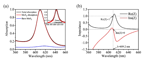
It is well know that in order to enhance absorption, the common method is to use resonances, but in the visible range, the monolayer TMDCs do not have strong resonant behavior. Therefore, the TMDC layer is inserted into the designed resonant structure to take advantage of the resonance in the structure. In addition, the atomically thin monolayer MoS2 has a high light transmission in the visible range, which causes minimal interference to the behavior of the resonator. As shown in Fig. 2(a), simulation results show that the calculated absorption spectra of the entire MPA and the contribution from MoS2 at the normal TM-polarized light, where nm, nm, nm, and nm, respectively. Simultaneously, the corresponding spectra of a bare MoS2 suspended in air also is given for a better comparison. It is found that the incident light is completely absorbed by the whole MPA (black line) at the resonant wavelength of 609.2 nm, among which about absorption (red line) occurs in MoS2. And the light absorption is improved by approximately times more than that of a bare MoS2 monolayer (blue line). In order to theoretically verify the numerical results, the coupled mode theory (CMT) can be used to describe both enhancement and suppression of light absorption[27]. In addition, for our chosen subwavelength structure, only the zero-order guided mode resonance can be excited and all other higher orders will not exist, which corresponds to a sharp peak in the absorption spectrum in Fig. 2(a). We assume a resonator, as shown in Fig. 1, has the amplitude of the input and output waves of and at a single resonance at , respectively. The external leakage rate of the resonator and the inherent loss rate of monolayer MoS2 are assigned to and , respectively, and the reflectivity of the entire system can be approximately described by the following equation[8],
| (1) |
and light absorption in a MPA is then calculated as
| (2) |
From the above equations, we note that when the system is in the state of resonance (), and the external leakage rate is the same as the inherent loss rate (), which corresponds to the critical coupling state of the system. At this point, the reflection coefficient of a whole MPA disappears and all incident light is absorbed. As shown in the inset of Fig. 2(a), in the vicinity of the resonance, the numerical simulations (FDTD-simulated) are in agreement with the theoretical calculations (CMT-fitted) under the critical coupling condition. However, we note that there are some deviations between the simulation and the theory at the far from the resonant wavelength region because the theory assumes a lossless resonator at this time. On the other hand, from the point of view of macroscopic electromagnetism, when the critical coupling condition is satisfied, the impedance of the whole structure should be equal to that of the free space (). The effective impedance () of the entire MPA can be expressed as[28]
| (3) |
The values of the -matrix elements can be calculated from the -matrix elements as well:
| (4) |
| (5) |
| (6) |
| (7) |
Where and represent the scattering () matrix and the transfer () matrix of the whole structure, respectively. And the two roots of the effective impedance () equation correspond to the two paths of light propagation, where we take the plus sign to represent the positive direction in Eq. (3). As shown in Fig. 2(b), at the resonance wavelength of 609.2 nm, the effective impedance of the structure perfectly matches the free space impedance (), achieving the perfect absorption of the entire structure, in which the basic principle is to minimize the reflectivity through impedance matching with free space (), and to eliminate the light transmittance by a metallic mirror with a certain thickness. In other words, when the incident light is coupled with the guided mode resonance of the designed structure, in the vicinity of the resonant wavelength, the electric field intensity near the monolayer MoS2 is obviously enhanced, which significantly boosting the light-matter interaction, and the light absorption in MoS2 can be greatly improved. In addition, under the critical coupling condition, the light absorption in monolayer MoS2 can reach the maximum value, and all incident light is completely absorbed by the whole structure at the same time. As depicted in Fig. 3(a) and 3(b), when the resonant cavity is in on-resonant ( nm) state, the electric field () near the monolayer MoS2 is strongly enhanced under the critical coupling condition as shown in Fig. 3(a). On the contrary, when the resonant cavity is in off-resonant (namely, nm) state, the reflection coefficient of a lossless system can be equivalent to -1, and the distribution of electric field intensity is shown in Fig. 3(b).

As mentioned above, we have used the guided resonance to realize critical coupling and achieved the ultra-high-efficiency light absorption of monolayer MoS2 in a MPA. We subsequently turn to investigate the dependence of the critical coupling on the structure parameters of the MPA. In the wavelengths of interest, the inherent loss of the structure mainly comes from MoS2, whose absorption is largely independent of the wavelength as shown in Fig. 2(a). Consequently, for the design principle of critical coupling, we can concentrate on controlling the external leakage rate of the structure, mainly through the following three parameters. First of all, as shown in Fig. 4(a) and 4(d), the influence of the air holes radius on the absorption spectra of a MoS2 monolayer (dashed lines) and the whole MPA (solid lines) is presented. From Fig. 4(a), we can see that even though the radius of the air hole is adjusted, the system is still in a critical coupling state, and the absorption peak of resonant wavelength exhibits a blue-shift with increasing the radius of air hole, which is due to the decrease of the effective refractive index of the structure with the expansion of the air hole. Moreover, as depicted in Fig. 4(d), we can also see that the influence on absorption peak (red line) and peak wavelength (black line) when the radius of air hole increases from nm to nm, where the peak wavelengths are linearly tuned by the radius of air hole, and the trend of absorption peak also shows that the system develops from undercoupling to critical coupling and then to over-coupling. Next, we consider the effect of the thickness of the PMMA layer on light absorption of monolayer MoS2 (dashed lines) and the whole structure (solid lines). As shown in Fig. 4(b), compared with the previous parameter , the thickness of PMMA layer is adjusted with the same spacing ( nm), and the wavelength of the absorption peak is almost unchanged while the system is always in critical coupling. Fig. 4(e) shows the calculated peak absorption (red line) and peak wavelength (black line) as functions of the PMMA layer thickness. It has been found that the peak absorption of more than can be maintained when the PMMA layer thickness () ranges from nm to nm while other parameters are fixed as in Fig. 1. Meanwhile, the peak wavelength of the structure is almost invariable and maintain approximately linear relationship with the PMMA layer thickness. The main reason is that the external leakage rate () of the structure is insensitive to the variation of the PMMA layer thickness in a certain range. We also consider the dependence of light absorption of monolayer MoS2 and the entire structure on the thickness of SiO2 layer in Fig. 4(c) and 4(f). We can find that when the thickness of SiO2 layer is adjusted at the same distance, the absorption spectrum of the structure exhibits a significant red-shift with increasing the thickness of SiO2 layer (), and the absorption peak also changes slightly, as shown in Fig. 4(c). It can be seen in Fig. 4(f) that the absorption peak of the structure slowly rises up, and then drastically falls down when increases. The maximum appears in the critical coupling state of nm, which indicates that the external leakage rate is sensitive to the change of the SiO2 layer thickness. Meanwhile, the relationship between peak wavelength and thickness of SiO2 layer is still nearly linear. To sum up, it can be seen that the designed structure has relatively large fabrication tolerances, and the tunable ultra-high-efficiency light absorption of monolayer MoS2 in a MPA at the wavelengths of interest can be achieved by adjusting the above three parameters properly.

In addition, it is easy to find that the structure we designed has the nice property of being polarization-independent under normal incidence, due to its rotational symmetry. Meanwhile, we further investigate the light absorption of monolayer MoS2 with different incident angle for TM-polarization and TE-polarization, respectively. From Fig. 5(a), we can find that the absorption of MoS2 for TM-polarization remains almost invariant when the angle of incidence varies from to , which is because the guided mode resonance is insensitive to the incident angle in this case[29]. In contrast, for TE-polarization, as shown in Fig. 5(b), the resonance exhibits wavelength splitting, and two major absorption peaks of the same degree appear in the absorption spectrum under oblique incidence, which forming multiple resonance. The two major absorption peaks originate from the excitation of other guided mode resonances, and they are sensitive to the incident angle, which is an important consideration in multispectral light detection[27].

Finally, we also consider the general effects of the proposed critical coupling scheme on light absorption of other monolayer TMDCs materials, such as MoSe2, WS2, and WSe2. FDTD simulations show that the absorption spectra of the designed TMDC-based perfect absorption system with different structural parameters under normal incidence, in which the monolayer MoS2 is replaced by the monolayer MoSe2, WS2, and WSe2, respectively. The total absorption of the structure (black lines) and the contribution from monolayer TMDCs (red lines), compared to the absorption of bare TMDCs stand in air (blue lines), as shown in Fig. 6. In addition, in the numerical simulations, the thickness of monolayer MoSe2, WS2, and WSe2 are set to nm, nm, and nm, respectively. And the corresponding dielectric constant are derived from the experimental measurement of Li et al[26]. For comparison, structure , structure , and structure represent a MPA with monolayer MoSe2 (for nm, nm, and nm) in Fig. 6(a), a MPA with monolayer WS2 (for nm, nm, and nm) in Fig. 6(b), and a MPA with monolayer WSe2 (for nm, nm, and nm) in Fig. 6(c), respectively. Absorption spectra corresponding to the above three structures show that the absorption of light in monolayer TMDCs can significantly reach , , and , respectively. And the corresponding absorption peaks appear at nm, nm, and nm, respectively. Certainly, we can also change the operating wavelength by adjusting the structure parameters to achieve the wavelength selectivity of the system, which is the same as that of MoS2. Therefore, the proposed TMDC-based perfect absorption system with its unique design principle can be applied to boost the absorption of other D monolayer materials.
4 Conclusions
A simple multilayer architecture with MoS2 embedded in a MPA is proposed and its light absorption properties are numerically investigated. Absorption above in monolayer MoS2 is obtained, which is over times more than that of bare monolayer MoS2. The absorption enhancement of monolayer MoS2 is mainly due to the strong confinement of electromagnetic field through the principle of critical coupling with guided resonance and the suppression of the loss caused by reflection and transmission in MPA. The operating wavelength can be modulated by adjusting the radius of air hole and the thickness of the PMMA and SiO2 layers, which are valuable for the tunability and selectivity of the high efficiency absorption of monolayer MoS2. Furthermore, the polarization independence of the structure at normal incidence and the angular characteristics of the system at oblique incidence are discussed by simulations. The geometry proposed here is general and can be extended with other monolayer TMDCs, such as MoSe2, WS2, and WSe2. Our investigation provides guidance for the device design of using critical coupling theory to improve the optical response of monolayer TMDCs, and our results may be of great significance for TMDC-based applications, such as photodetection and photoluminescence.
Funding
This work is supported by the National Natural Science Foundation of China (Grant No. 61376055 and 61775064), and the Fundamental Research Funds for the Central Universities (HUST: 2016YXMS024).