A Multi-Kernel Multi-Code Polar Decoder Architecture
Abstract
Polar codes have received increasing attention in the past decade, and have been selected for the next generation of wireless communication standard. Most research on polar codes has focused on codes constructed from a polarization matrix, called binary kernel: codes constructed from binary kernels have code lengths that are bound to powers of . A few recent works have proposed construction methods based on multiple kernels of different dimensions, not only binary ones, allowing code lengths different from powers of . In this work, we design and implement the first multi-kernel successive cancellation polar code decoder in literature. It can decode any code constructed with binary and ternary kernels: the architecture, sized for a maximum code length , is fully flexible in terms of code length, code rate and kernel sequence. The decoder can achieve frequency of more than GHz in nm CMOS technology, and a throughput of Mb/s. The area occupation ranges between mm2 for and mm2 for . Implementation results show an unprecedented degree of flexibility: with , up to code lengths can be decoded with the same hardware, along with any kernel sequence and code rate.
Index Terms:
polar codes, multi-kernel, successive-cancellation decoding, hardware implementation.I Introduction
Polar codes are capacity-achieving error correcting codes, characterized by a low-complexity encoding and decoding process [1]. They have been chosen to be adopted in the fifth generation of wireless communication standards (5G) [2], that foresees a variety of scenarios. Thus, coding schemes targeting low latency, low power, and high performance must be devised. Error correction performance and decoding speed are heavily influenced by the polar code block length, and the different scenarios demand a wide range of code lengths.
The majority of current research is focused on polar codes recursively constructed from a polarization matrix, also called a binary kernel [1]. The code lengths of polar codes constructed from binary kernels are bound to powers of . This is a strong limitation, that is currently overcome with rate-matching schemes [3, 4], whose performance and optimality is hard to evaluate a priori. A few recent works have proposed construction methods based on multiple kernels of different dimensions [5, 6, 7]. Multi-kernel polar codes can have block lengths different from powers of , at the cost of more complex decoding algorithm update rules. In [6], it has been shown that multi-kernel codes can outperform codes of the same length obtained through the application of state-of-the-art puncturing and shortening schemes. At a frame error rate (FER) of almost , multi-kernel codes yield gains ranging from dB to dB.
Polar code decoder architectures in literature focus mainly on design-time flexibility [8, 9, 10], with parametrized designs that can be implemented to decode a particular code. Some decoders guarantee code-rate online flexibility [11, 12, 13, 14]: while the decoder can decode a single code length, any code rate is supported with the same hardware. The decoder architectures presented in [15, 16] target binary kernels only, and are online flexible in terms of both code rate and code length. However, a different decoding program must be stored for every considered combination of code length and rate, leading to huge area occupation. The unrolled architecture presented in [17] can decode a small set of binary nested code lengths and rates.
In this work, we consider multi-kernel polar codes constructed from binary and ternary () kernels, and we propose a flexible decoder architecture. The presented design can decode any code constructed from any combination of binary and ternary kernels, up to a maximum code length defined at design time, and any code rate. It is the first multi-kernel decoder in literature, yielding an unmatched degree of flexibility, with up to 55 supported code lengths in the considered case study. Implementation results in nm CMOS technology show an achievable frequency of more that GHz and Mbps coded throughput.
The remainder of the paper is organized as follows. In Section II, we introduce polar codes construction and decoding, while in Section III we show the error-correction performance of some multi-kernel codes. Section IV details the proposed decoder architecture, while implementation results are given in V, together with a comparison with the state of the art. Conclusions are drawn in Section VI.
II Preliminaries
II-A Polar Codes
A polar code is a linear block code of length and rate , that relies on a phenomenon called channel polarization [1]. When tends to infinite, the symmetric capacity of each bit-channel tends towards either or , thus identifying very reliable and very unreliable channels.
Let us assume , where , and let be the -bit vector input to the encoder. The information bits are assigned to the most reliable channels of , while the remaining are fixed to a known value (usually ), and are known as frozen bits. The ensemble of their indices is the frozen set .
The encoding process can be represented through the linear transformation , where is the generator matrix, expressed through the n-th Kronecker product of the matrix . The matrix is a binary polarization matrix, or kernel, defined as follows:
From the definition of , the recursive nature of the encoding process can be noticed: a polar code of length can in fact be obtained as the concatenation of two polar codes. Polar code encoding can also be portrayed through a Tanner graph, as shown in Fig. 1 for an code. Each stage depicts a Kronecker product, and the dashed boxes represent each operation. Between neighbouring stages permutations are inserted, in which the bit-indices of the inputs are cyclically rotated to the right by one place [1].
II-B Successive Cancellation Decoding
In [1] a first successive cancellation (SC) decoding algorithm has been proposed. It can be represented as a binary search tree where all the nodes must be explored, with priority being given to left branches. An example of a polar code SC decoding tree is shown in Fig. 2(a): the leaf nodes at stage can be either information bits (dark gray) or frozen bits (light gray).
Let us call the vector of logarithmic likelihood ratios (LLRs) obtained at the channel output, and the estimated vector output by the decoder. The decoding starts from the root node, and at each node information is passed from parent to child according to the scheme shown in Fig. 2(b). The LLR value is received and used to compute , then is obtained and used to compute . Once is available, can be computed. Once a leaf node is reached, the value of is estimated. If index , its value is set to , otherwise a hard decision on the sign of is performed. Calling the length of the polar code at stage , we can define :
| (1) |
| (2) |
| (3) |
where represents the XOR operation and is a function returning the sign of the argument. In (1), both the exact and the approximate (hardware-friendly) computation, proposed in [8], are shown. At leaf nodes, is initialized as (4), where is the index identifying the current leaf node.
| (4) |
II-C Multi-kernel construction
In [6] a generalized construction method for polar codes has been presented: together with , larger kernels have been investigated. Thus, the matrix is composed of a series of Kronecker products between kernels of different sizes. Ternary kernels, i.e. kernels of dimensions , have been considered in [6], where the proposed polarization matrix is
Fig. 3 portrays the Tanner graph for an code constructed with a kernel sequence . As in the binary case, inter-stage permutations are required to reshuffle indices. For each stage , the permutation matrix can be found as
where is the so-called canonical permutation introduced in [6], , and are the dimensions of the -th kernel of the Kronecker product. Finally, is computed in order to re-align output indices with those relative to the encoder input, considering all the previous permutations.
Fig.4(a) shows the SC decoding tree for the same code, and the message passing criterion in case of ternary nodes is shown in Fig. 4(b). Defining (1) as , (2) as , and (3) as , for a ternary node at stage the decoding rules are:
| (5) |
| (6) |
| (7) |
| (8) |
Similarly to the binary kernel case, we define (5), (6), (7) and (8) as , , and respectively.
III Multi-kernel codes
The multi-kernel code construction method proposed in [6] yields substantial error-correction performance gain with respect to puncturing and shortening schemes. Table I reports such gain when two multi-kernel codes are compared to codes obtained with the puncturing method in [18] and the shortening method in [19], for SC decoding and list SC (SCL) [20] with a list size of . Depending on the target FER, the gain ranges from 0.1 to 1.1 dB.
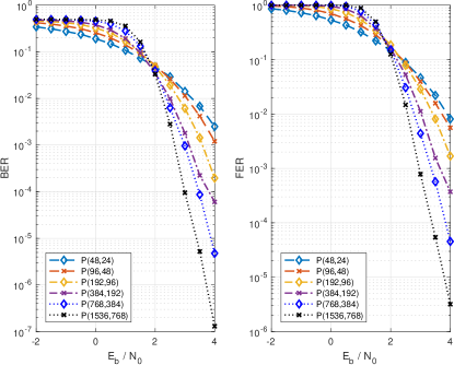
Using the construction method described in [6], multi-kernel codes have been constructed. Their error-correction performance has been simulated through a binary-input additive white Gaussian noise (AWGN) channel with binary phase-shift keying modulation. The bit error rate (BER) and FER curves are shown in Fig. 5, obtained with SC decoding and LLRs represented in double-precision floating-point format. As discussed in [6, 7], the Kronecker product is not commutative, and different kernel orders will results in different codes. However, there is currently no theoretical way to identify the best kernel multiplication order: thus, the different kernel orders need to be simulated to identify the one that gives the best error-correction performance. In the remainder of our work, we considered the following codes and kernel orders, obtained with the method described in [7]:
-
•
with
-
•
with
-
•
with
-
•
with
-
•
with
-
•
with
| SC | SCL | |||
| FER | ||||
| [6] VS puncturing [18] | 0.20 dB | 0.45 dB | 0.20 dB | 0.25 dB |
| [6] VS shortening [19] | 0.45 dB | 0.70 dB | 0.65 dB | 1.10 dB |
| SC | SCL | |||
| FER | ||||
| [6] VS puncturing [18] | 0.10 dB | 0.25 dB | 0.35 dB | 0.50 dB |
| [6] VS shortening [19] | 0.15 dB | 0.35 dB | 0.75 dB | 0.80 dB |
IV Decoder Architecture
We propose a multi-code semi-parallel SC decoder which supports purely-binary, purely-ternary and binary-ternary mixed construction polar codes. The architecture is sized with a maximum code length , and can support any code length that can be expressed as a combination of binary and ternary kernels, and any code rate. For mixed polar codes, the architecture can decode codes constructed with any kernel order, without knowledge of the code structure at design time.
The overall decoder architecture is shown in Figure 6. It relies on processing elements (PEs) implementing (1)-(8), and dedicated memories for channel and internal LLRs, values and candidate codeword. Both channel and internal LLRs are represented on bits, of which are assigned to the fractional part.
Together with the code length, the decoder receives as inputs the following parameters:
-
•
information about binary and ternary stages;
-
•
memory address offsets for both LLRs and values, relative to the current code length;
-
•
number of steps required by each stage to process all inputs given the number of PEs. This is due to the fact that the decoder has a semi-parallel architecture and, for stages where , the number of PEs is not sufficient to elaborate all data in a single clock cycle.
In order to simplify and reduce both memory accesses and routing, the architecture has been designed for bit-reversed polar codes [8]. This approach allows to dramatically simplify the memory accesses.
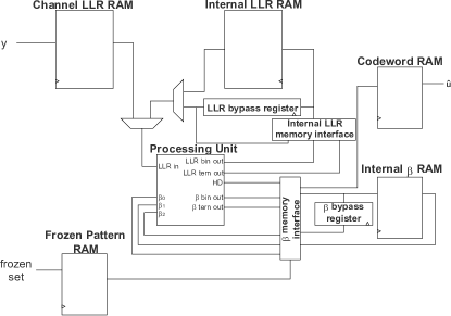
IV-A Data flow
The channel output is initially stored in the Channel LLR RAM, while the frozen set and the code parameters listed in the previous section are uploaded to their dedicated memories, respectively the Frozen Pattern RAM and a set of registers. For operations involving soft values, the Processing Unit receives as input either the channel or the internal LLRs, according to the current stage of the decoding tree. For operations (3)-(8), data read from the Internal RAM are used. Results are stored either in the Internal LLR RAM or in the Internal RAM, according to the performed operation. When a leaf node is reached and a hard decision (HD) is performed to decide the value of a bit (4), the result is stored in the Codeword RAM. The decoding phase ends when the bit associated to the rightmost leaf node is estimated: the decoded codeword is thus output.
IV-B Processing Unit
The Processing Unit (PU) is the computational core of the decoder, where all the operations are performed: (1), (2), (3), (5), (6), (7) and (8). It contains processing elements (PEs) and combine blocks (CBs) organized as follows:
-
•
binary-ternary mixed PEs, each of them able to compute any or operations, both binary and ternary;
-
•
binary PEs, which support only and ;
-
•
binary-ternary mixed CBs which perform both and ;
-
•
binary CBs, which support only .
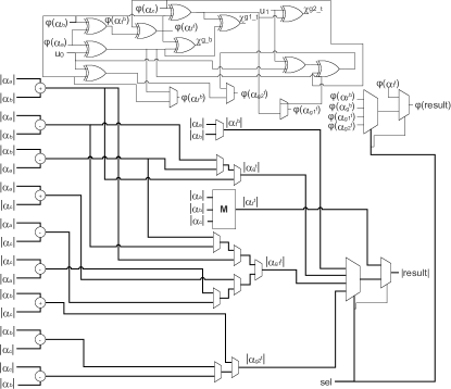
Since it has been observed that between binary and ternary operations there are common computations, mixed PEs are used to increase resource sharing, at the cost of a multiplexing operation; additional purely-binary PEs are used to align the number of used inputs both for binary and ternary operations. Thus the maximum number of elaborated soft inputs is fixed to , while the results are either or LLRs: in fact it can be noticed that the number of operations simultaneously performed is in the binary case and in the ternary one. For binary operations each -th PE elaborates the -th and -th LLR inputs, while for ternary ones each -th mixed PE uses LLRs corresponding to indices , and . The same holds for CBs. From the last considerations must be a multiple of ; an example of PU with is shown in Fig. 7.
Although there are situations in which not all PEs are performing useful computations, inputs are nevertheless elaborated and stored in the corresponding memory. Unnecessary data are subsequently ignored in the final estimation: this happens for stages where is not a multiple of . The impact of two different LLR representations on the implementation cost of the PU has been evaluated: we have in fact designed PEs with both 2’s complement and sign and magnitude representations. FPGA synthesis results have shown that the sign and magnitude binary PE has lower resource requirements and shorter critical path than the 2’s complement one, while the sign and magnitude mixed PE has similar resource requirements and shorter critical path than the 2’s complement one. Thus, all LLRs in the proposed decoder are represented with sign and magnitude.
IV-B1 Binary Processing Elements
The architecture of binary PEs is the one proposed in [8]. Let us call and the input LLRs. For the hardware-friendly version of (1) operation the result computation is straightforward:
| (9) |
| (10) |
where is the operation result. Analyzing the complete truth table both for sign and magnitude of (2), its resulting equations are:
| (11) |
| (12) |
where
| (13) |
| (14) |
This architecture is shown in Figure 8 . Adders and subtractors saturate their result if outside the available range.
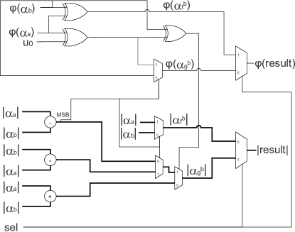
IV-B2 Binary-ternary mixed Processing Elements
An analysis analogous to the binary case has been conducted on (5), (6) and (7). The resulting equations are the following:
| (15) |
| (16) |
| (17) |
| (18) |
| (19) |
| (20) |
where
| (21) |
| (22) |
| (23) |
| (24) |
The circuit implementing these operations is shown in Figure 9, where again adders and subtractors can saturate the result. The block is a combination of pruned multiplexers selecting the minimum absolute value according to the already computed selection signals, which correspond to the most significant bits of the output of the subtractors.
Mixed PEs perform both binary and ternary operations, and need to select their input accordingly. Thus, LLR multiplexing logic is inserted at their input. This logic consists of two Q-bit multiplexers for each mixed PE.
IV-B3 Combine blocks
Both binary and binary-ternary mixed CBs are composed of XOR gates implementing and respectively, where is the binary/ternary selector.
IV-C Memory system
While efficient in terms of resource usage, register-based approaches like [11] lead to excessive area occupation. Thus, this design foresees the usage of SRAM banks. The width of these memories is different from that of memories in a purely-binary decoder design, since they have to accommodate ternary operations and their concurrent input and output volume. Additionally, for Internal LLR RAM a three-bank solution has been implemented, since ternary-kernel functions are supported: for purely-binary decoders two banks would have been sufficient.
IV-C1 Channel LLR RAM
This memory stores the LLRs coming from the channel. Each memory word is long, since for each operation involving LLRs of them are required by the PU. Its depth is . This memory uses two separate ports, one for reading and one for writing.
IV-C2 Internal LLR RAM
It contains the partial results of and operations. Similarly to the Channel LLR RAM, the parallelism must be . The computation of the depth takes into account that for each decoding stage only one LLR vector must be stored: once the node which took as input the computed LLR has generated its output , that soft value will be no longer used and can be overwritten. In addition, for stage it is not needed to memorize the result since the hard decision is performed in the same clock cycle.
The memory depth is computed as:
Also for this memory two separate ports for reading and writing are required.
It is possible to rearrange the Internal LLR RAM with a bank structure. However, due to the variable number of data that needs to be written, depending on the stage being binary or ternary, four banks with two different widths should be implemented. This would incur significant control and addressing overhead, with no tangible advantage with respect to the proposed structure. More details on the handling of different result sizes are given in Section IV-D.
IV-C3 Internal RAM
This memory stores all values computed inside the decoding tree; it is organized in three banks, which share the same input writing bus:
-
•
bank0 for : it is equal to in both binary and ternary cases;
-
•
bank1 for : it is equal to for binary stages, while for ternary ones it represents ;
-
•
bank2 for : it corresponds to the ternary stages .
The bank organization is fundamental for parallel data reading in , and operations. Each bank has a width of since results of operations are on bits, while their depths are equal to:
IV-C4 Codeword RAM
It is used to store the decoder output , composed by the HDs performed at the leaf nodes. Its width is a design choice independent from all other parameters, while the depth is
IV-C5 Frozen Pattern RAM
It stores the frozen set, where each of bits identifies if the corresponding bit-channel is frozen or not. The memory width is an independent design choice, while the depth can be expressed as
Table II reports the breakdown of the memory requirements for the proposed decoder with various , and combinations. To correctly evaluate the memory overhead brought by the multi-kernel approach, the memory sizes for purely binary polar decoders with similar parameters have been detailed as well. It can be seen that most of the additional memory bits can be found in the internal memory.
| MK | PB | MK | PB | MK | PB | |
|---|---|---|---|---|---|---|
| [bit] | [bit] | [bit] | [bit] | [bit] | [bit] | |
| Channel LLR RAM | 30240 | 28672 | 6480 | 6144 | 1440 | 1280 |
| Internal LLR RAM | 43680 | 39424 | 11520 | 9984 | 1980 | 1760 |
| Internal RAM | 31680 | 19456 | 9000 | 5376 | 2052 | 1216 |
| Codeword RAM | 4096 | 4096 | 1024 | 1024 | 256 | 256 |
| Frozen Pattern RAM | 4096 | 4096 | 1024 | 1024 | 256 | 256 |
| Total | 113792 | 95744 | 29048 | 23552 | 5984 | 4768 |
IV-D Memory interfaces
Two interfacing modules are required to adapt the inherent parallelism of the memories to that of the PU.
IV-D1 Internal LLR memory interface
Fig. 10 shows the interface circuit. It is tasked with choosing, during write operations, which part of the memorized word has to be overwritten. In fact, the results of and operations are or LLR, for binary and ternary cases respectively, while the width of the LLR memories is . Each memory location takes two or three clock cycles to be overwritten with useful data. So, at tree stages where and the PU takes more than one clock cycle to process them, the following steps are performed:
-
•
For binary stages:
-
1.
The -th operation result ( LLRs) is stored in the memory together with appended zeros;
-
2.
The -th operation result is stored after the most significant bits of the previously written word, so that the padding zeros are overwritten and the new stored word contains the results of both the -th and -th operations.
-
1.
-
•
For ternary stages:
-
1.
The -th operation result ( LLRs) is stored in the memory together with appended zeros.
-
2.
The -th operation result is stored after the most significant bits of the previously written word. The new word contains the results of both the -th and -th operations;
-
3.
The -th operation result is stored after the previously written bits, completing the LLR word.
-
1.
To overwrite only parts of the previously written word, the bypass buffer output is used. When , the results are stored in the first part of the word as usual; the remaining bits are not considered in subsequent operations.
IV-D2 memory interface
Figure 11 shows the interface architecture. It is used both for reading and writing from the Internal RAM:
-
•
Reading: operations involving values need either or bits per bank as input, while each word is composed of bits. Thus, the relevant word parts are selected according to the actual number of elaborated LLRs for that node.
-
•
Writing: the data is selected between the CB results and the HD for the leaf nodes.
IV-E Bypass registers
Two bypass registers must be used since the memory system is RAM-based and, if a result is computed and ready to be stored at the -th clock cycle, it can be correctly read only from the ()-th cycle onwards, to avoid incurring conflicts. So, for all the nodes at stage , bypass registers allow reading newly computed data already at the following clock cycle. A -bit register is used for the Internal LLR RAM, while a second -bit register is necessary for the Internal RAM.
IV-F Control Unit
The Control Unit provides all the memory addresses to the memories and control signals to the datapath. It has been designed as several hierarchically controlled finite state machines. The decoding process follows the same approach of the tree exploration by means of different counters, which keep track of the status and of the number of visited leafs. The decoding process ends when a number of leafs equal to the code length has been visited.
IV-G Multi-code support
Memories are sized for a maximum code length , but any code length , with a multiple of or is supported. Memory requirements are upper bounded by the largest combination of kernels leading to , since a higher number of stages are present in the decoding tree than in a mixed-kernel polar code with similar code length. The input code parameters allow to know when the leaf node stage is reached, and thus when the tree ascension has to start. The status counter in the CU uses foreknowledge of the number of kernels and their dimension to schedule the right operation at each stage: thus, any code rate and kernel order can be decoded without any change to the hardware. The total amount of bits required to store the code parameters for a code of length is , where is the number of kernel composing the code. The PU has been designed independently of the code length.
V Implementation Results
The decoder architecture illustrated in the previous Section has been described in VHDL, verified with ModelSim, and synthesized with Cadence RTL Compiler on TSMC 65nm CMOS technology node.
The choice of the number of LLR quantization bits influences a substantial part of the computational hardware and memory width. In Figure 12 the error-correcting performance of a polar code is shown: between and curves there is not a significant difference, while choosing leads to larger error figures with respect to floating point precision. Although the number of fractional bits does not influence the hardware architecture, a high requires a higher . In Figure 12 we can notice that yields only minor FER degradation. Thus, for we chose and . Similar studies were performed in case of and , leading to , in the first case and to , in the second.
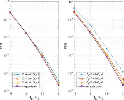
Table III reports synthesis results for three sets of decoder parameters. Along with the parameters, the number of supported code lengths and the maximum achievable frequency are shown. All implementations can run at more than one GHz. The is the area occupation when all memories are synthesized as registers, while in all the memories are implemented as SRAM. For both estimations the logic and memory cells area percentages are shown.
| 55 | 40 | 27 | ||
| [GHz] | 1.06 | 1.11 | 1.23 | |
| [mm2] | 2.63 | 0.62 | 0.14 | |
| Combinational | [%] | 45.0 | 38.9 | 40.3 |
| Sequential | [%] | 55.0 | 61.1 | 59.7 |
| [mm2] | 2.01 | 0.46 | 0.11 | |
| Combinational | [%] | 58.9 | 56.7 | 55.2 |
| Registers | [%] | 28.6 | 28.9 | 31.2 |
| RAM | [%] | 12.5 | 14.4 | 13.6 |
The latency of the decoding phase depends on the number of PEs, on the number of kernels , on the kernels dimension and their order.
The decoding latency, measured in clock cycles (CCs) can be computed as:
| (25) |
In Table IV some polar code timing performance are shown, where is the decoding latency, is the achievable frequency, and the coded throughput. They consider a wide range of code parameters over three different decoder implementations. Since the kernel order impacts the decoding latency, dimension of each kernel has been reported, from left to right as in the Kronecker product. It is possible to see that the achievable frequency is consistently above 1 GHz, and that the coded throughput ranges from to Mbps.
| code | decoder | |||||
|---|---|---|---|---|---|---|
| parameters | parameters | [CCs] | [GHz] | [bpc] | [Mbps] | |
| {2,3,2,2,2,3,3,3,3} | 7965 | 1.06 | 0.49 | 519.4 | ||
| =120 | =7 | |||||
| {2,3,3,2,3,3,3,3} | 5953 | 1.06 | 0.49 | 519.4 | ||
| =120 | =7 | |||||
| {2,2,2,2,2,2,3,3,3} | 3548 | 1.06 | 0.49 | 519.4 | ||
| =120 | =7 | |||||
| {3,2,2,2,2,2,2,2,2,2} | 4663 | 1.06 | 0.33 | 350.6 | ||
| =120 | =7 | |||||
| {2,2,3,2,2,2,2,2,2} | 2326 | 1.11 | 0.33 | 366.5 | ||
| =60 | =6 | |||||
| {2,2,2,2,2,2,3,3} | 1234 | 1.11 | 0.47 | 521.7 | ||
| =60 | =6 | |||||
| {3,2,2,2,2,2,2,2} | 1156 | 1.11 | 0.33 | 368.7 | ||
| =60 | =6 | |||||
| {2,2,3,3,3,3} | 652 | 1.11 | 0.50 | 555.0 | ||
| =60 | =6 | |||||
| {3,3,3,3,3} | 519 | 1.23 | 0.47 | 578.1 | ||
| =18 | =5 | |||||
| {3,2,2,2,2,2,2} | 587 | 1.23 | 0.32 | 402.3 | ||
| =18 | =5 | |||||
| {2,2,2,3,2,2} | 272 | 1.23 | 0.35 | 434.1 | ||
| =18 | =5 | |||||
| {3,3,3,3} | 162 | 1.23 | 0.50 | 615.0 | ||
| =18 | =5 | |||||
| {3,2,2,2,2} | 137 | 1.23 | 0.35 | 430.9 | ||
| =18 | =5 | |||||
In Table V the implementation results of the proposed decoder have been compared to rate-flexible purely binary decoders in the state of the art, since to the best of our knowledge this is the first multi-kernel decoder in literature. All decoders have been implemented with 65 nm CMOS technology, and target a code with , that for our work corresponds to as well. Both in [8] and [10] semi-parallel architectures are proposed, supporting the SC algorithm and a single fixed code length. The reported results for [10] refer to their best devised architecture, called folded high performance partial sum network. It limits the number of processing elements by folding highly parallel operations and performing them in several clock cycles, thus increasing hardware utilization. Observing the bit-per-cycle (bpc) throughput in Table V, it can be noticed that both [8] and [10] outperform the proposed decoder for the considered purely binary codes. The reason can be found in the additional clock cycles required for operations in our architecture: since different kernel orders are supported, the sequence of (3) and (8) is not always the same. Thus, it is not possible to hardwire an XOR tree to compute the at all stages in one clock cycle, like in decoders supporting only binary kernels: separate clock cycles are spent to perform the operations according to the correct kernel order. On the other hand, [8] and [10] consider only binary kernels and, implementing a tree of operations and eventually selecting a partial result, values are computed in the same clock cycle immediately after the . This is not affecting the critical path in a significant way since only few XOR gates are added. As shown in Table IV, codes constructed with higher-dimension kernels yield a higher throughput. When decoding a ternary node, due to the higher utilization factor of the PEs and the higher number of useful computations in each clock cycle, the number of clock cycles needed to decode a codeword is lower. Moreover, latency-reduction techniques like the ones presented in [21, 9] can be easily adapted to the proposed architecture.
The proposed decoder yields a higher area occupation than both [8] and [10]. This is mainly due to the higher quantization parameter and to the support to ternary functions. Mixed PEs require LUTs on FPGA and area occupation with respect to the purely binary ones. However, our decoder is completely code-length flexible and supports multiple kernel sizes, any code rate and any kernel order. Moreover, it can achieve the highest frequency among the considered works, and a higher throughput in Mbps than [8].
Semi-parallel SC-based decoders in literature, while supporting only binary kernels and often being designed targeting a single code, share the basic multi-PE structure of our work. For the sake of completeness, in Table V we consider also [13] and [17]. These architectures are very different from semi-parallel decoders, but guarantee a certain degree of flexibility. The decoder in [17] can decode a fixed set of combinations of code lengths and code rates, while the architecture proposed in [13] is rate-flexible. Both architectures are able to achieve a higher throughput than the proposed decoder, at the cost of larger area occupation and a lower degree of flexibility.
VI Conclusion
In this work, we have proposed the first polar code decoder architecture supporting kernels of different sizes. It implements the successive cancellation algorithm, and can support any code rate, any sequence of binary and ternary kernels and any code length that can be expressed as a combination of binary and ternary kernels. The decoder can achieve a frequency of more than a GHz in 65 nm CMOS technology, and a throughput of Mb/s. The area occupation ranges between mm2 for and mm2 for . Implementation results show an unprecedented degree of flexibility: with , up to 55 code lengths can be decoded with the same hardware, along with any kernel sequence and code rate.
References
- [1] E. Arıkan, “Channel polarization: A method for constructing capacity-achieving codes for symmetric binary-input memoryless channels,” IEEE Trans. Inf. Theory, vol. 55, no. 7, pp. 3051–3073, July 2009.
- [2] “Final report of 3GPP TSG RAN WG1 #87 v1.0.0,” http://www.3gpp.org/ftp/tsg_ran/WG1_RL1/TSGR1_87/Report/Final_Minutes_report_RAN1%2387_v100.zip, Reno, USA, November 2016.
- [3] L. Chandesris, V. Savin, and D. Declercq, “On puncturing strategies for polar codes,” in 2017 IEEE International Conference on Communications Workshops (ICC Workshops), May 2017, pp. 766–771.
- [4] V. Bioglio, F. Gabry, and I. Land, “Low-complexity puncturing and shortening of polar codes,” CoRR, vol. abs/1701.06458, 2017. [Online]. Available: http://arxiv.org/abs/1701.06458
- [5] N. Presman, O. Shapira, S. Litsyn, T. Etzion, and A. Vardy, “Binary polarization kernels from code decompositions,” IEEE Transactions on Information Theory, vol. 61, no. 5, pp. 2227–2239, May 2015.
- [6] F. Gabry, V. Bioglio, I. Land, and J. C. Belfiore, “Multi-kernel construction of polar codes,” in 2017 IEEE International Conference on Communications Workshops (ICC Workshops), May 2017, pp. 761–765.
- [7] V. Bioglio, F. Gabry, I. Land, and J. Belfiore, “Minimum-distance based construction of multi-kernel polar codes,” CoRR, vol. abs/1701.07616, 2017. [Online]. Available: http://arxiv.org/abs/1701.07616
- [8] C. Leroux, A. Raymond, G. Sarkis, and W. Gross, “A semi-parallel successive-cancellation decoder for polar codes,” IEEE Trans. Signal Process., vol. 61, no. 2, pp. 289–299, January 2013.
- [9] B. Yuan and K. K. Parhi, “Low-latency successive-cancellation polar decoder architectures using 2-bit decoding,” IEEE Transactions on Circuits and Systems I: Regular Papers, vol. 61, no. 4, pp. 1241–1254, April 2014.
- [10] Y. Fan and C. y. Tsui, “An efficient partial-sum network architecture for semi-parallel polar codes decoder implementation,” IEEE Transactions on Signal Processing, vol. 62, no. 12, pp. 3165–3179, June 2014.
- [11] S. A. Hashemi, C. Condo, and W. J. Gross, “A fast polar code list decoder architecture based on sphere decoding,” IEEE Trans. Circuits Syst. I, vol. 63, no. 12, pp. 2368–2380, December 2016.
- [12] ——, “Fast and flexible successive-cancellation list decoders for polar codes,” IEEE Transactions on Signal Processing, vol. PP, no. 99, pp. 1–14, 2017.
- [13] O. Dizdar and E. Arikan, “A hihg-throughput energy-efficient implementation of successive cancellation decoder for polar codes using combinational logic,” IEEE Trans. Circuits Syst. I, vol. 63, no. 3, pp. 436–447, March 2016.
- [14] T. Che, J. Xu, and G. Choi, “Tc: Throughput centric successive cancellation decoder hardware implementation for polar codes,” in 2016 IEEE International Conference on Acoustics, Speech and Signal Processing (ICASSP), March 2016, pp. 991–995.
- [15] G. Sarkis, P. Giard, A. Vardy, C. Thibeault, and W. Gross, “Fast polar decoders: Algorithm and implementation,” IEEE J. Sel. Areas Commun., vol. 32, no. 5, pp. 946–957, May 2014.
- [16] F. Ercan, C. Condo, and W. J. Gross, “Reduced-memory high-throughput fast-SSC polar code decoder architecture,” in 2017 IEEE International Workshop on Signal Processing Systems (SiPS 2017), to appear 2017.
- [17] P. Giard, G. Sarkis, C. Thibeault, and W. J. Gross, “Multi-mode unrolled architectures for polar decoders,” IEEE Trans. Circuits Syst. I, vol. 63, no. 9, pp. 1443–1453, September 2016.
- [18] K. Niu, K. Chen, and J. R. Lin, “Beyond turbo codes: Rate-compatible punctured polar codes,” in 2013 IEEE International Conference on Communications (ICC), June 2013, pp. 3423–3427.
- [19] R. Wang and R. Liu, “A novel puncturing scheme for polar codes,” IEEE Communications Letters, vol. 18, no. 12, pp. 2081–2084, Dec 2014.
- [20] I. Tal and A. Vardy, “List decoding of polar codes,” IEEE Trans. Inf. Theory, vol. 61, no. 5, pp. 2213–2226, May 2015.
- [21] C. Zhang, B. Yuan, and K. K. Parhi, “Reduced-latency SC polar decoder architectures,” in 2012 IEEE International Conference on Communications (ICC), June 2012, pp. 3471–3475.