Ge hole spin qubit
Abstract
Holes confined in quantum dots have gained considerable interest in the past few years due to their potential as spin qubits. Here we demonstrate double quantum dot devices in Ge hut wires. Low temperature transport measurements reveal Pauli spin blockade. We demonstrate electric-dipole spin resonance by applying a radio frequency electric field to one of the electrodes defining the double quantum dot. Next, we induce coherent hole spin oscillations by varying the duration of the microwave burst. Rabi oscillations with frequencies reaching 140 MHz are observed. Finally, Ramsey experiments reveal dephasing times of 130 ns. The reported results emphasize the potential of Ge as a platform for fast and scalable hole spin qubit devices.
IST Austria]Institute of Science and Technology Austria, Am Campus 1, 3400 Klosterneuburg, Austria IST Austria]Institute of Science and Technology Austria, Am Campus 1, 3400 Klosterneuburg, Austria IST Austria]Institute of Science and Technology Austria, Am Campus 1, 3400 Klosterneuburg, Austria JK University]Johannes Kepler University, Institute of Semiconductor and Solid State Physics, Altenbergerstr. 69, 4040 Linz, Austria IST Austria]Institute of Science and Technology Austria, Am Campus 1, 3400 Klosterneuburg, Austria
Spins in isotopically purified Si have shown record coherence times 1 and fidelities 2 making them promising candidates for scalable quantum circuits 3. One of the key ingredients for realizing such circuits will be a strong coupling of spins to superconducting resonators 4. This has been recently achieved for Si by dressing electrons with spin orbit coupling 5, 6. Holes, on the other hand, have intrinsically strong spin orbit coupling making them thus promising candidates for electrically controlled and scalable qubits. In 2016, the first hole spin qubit was reported in a Si FinFET 7. Beside Si, also Ge has emerged as an interesting material system due to the strong and tunable spin orbit coupling 8, 9, 10, 11 good contacts to superconductors 12, 13, 14 and relatively small effective mass. Indeed, in the past few years quantum dot (QD) devices in Ge/Si core/shell nanowires 15, 9, 16, 17, self-assembled nanocrystals 13 and Ge hole gases 14 have been reported. However, no qubit has been demonstrated so far.
In this letter, we demonstrate the ability to capture holes in double quantum dots (DQD) fabricated in Ge hut wires (HWs) 18, 19. We make use of the Pauli spin blockade (PSB) 20 mechanism and the electric-dipole spin resonance (EDSR) technique in order to demonstrate the addressability of single holes. By varying the duration of the microwave burst, Rabi oscillations with frequencies higher than 100 MHz have been observed. Finally, Ramsey fringes-like measurements reveal dephasing times of 130 ns, twice the dephasing time reported for holes in Si 7.
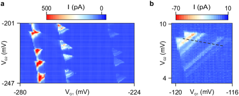
The stability diagram of a DQD device showing characteristic bias triangles is depicted in Fig. 1a with the two gate voltages and .
A representative measurement of two bias triangles from a second device is shown in Fig. 1b. Due to the fairly low mutual capacitance of about 1 aF they are merged already at relatively low bias voltages. The ground state as well as several additional excited states are clearly visible.
Energy level separations up to 1 meV and a relative lever arm are observed. Since the two top gates G1 and G2 are very close to the HW a relatively strong coupling is obtained, leading to alpha factors of and 21.
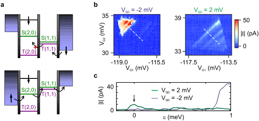
In order to realize a spin 3/2 qubit in our DQD devices we rely on Pauli spin blockade (PSB) 20 as a spin-selective read-out mechanism 22.
PSB occurs in a (1,1) (0,2) or an equivalent (2N-1, 2N-1) (2N-2, 2N) charge configuration (see Fig. 2a).
In such a configuration transport through the DQD is blocked due to spin selectivity even if it is energetically allowed. By reversing the applied source-drain bias voltage the spin blockade can be lifted. Signatures of PSB were observed in several bias triangles exhibiting a suppressed leakage current of the triangle baseline.
Two representative direct current (DC) measurements are shown in the left and right panel of Fig. 2b for bias voltages of -2 mV and +2 mV, respectively.
The corresponding line traces along the detuning direction (white dashed lines) are plotted below in Fig. 2c. In the blocked configuration (blue dotted line) the zero-detuning current, indicated by the black arrow, drops to about 2 pA compared to 10 pA in the non-blocked case (green solid line), as expected for PSB 22.
Rotating one of the spins can lift PSB. This can be achieved via the EDSR mechanism 23. An alternating current (AC) electric field applied to one of the gates of the DQD (here G1) can cause oscillations in the position of the confined hole wave function (see Fig. 3b). Such an oscillation in combination with a constant applied magnetic field can lead to spin rotations in systems with strong spin orbit coupling 22. In order to induce such continuous wave spin rotations the driving frequency of the AC electric field has to be equal to the Larmor frequency , where is the g-factor for a certain magnetic field orientation, is the Bohr magneton and is Planck’s constant.
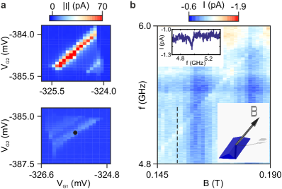
Fig. 3a shows a pair of bias triangles for positive and negative bias voltages from a third measured device.
The black circle in the lower panel of Fig. 3a indicates the position at which the EDSR measurement shown in Fig. 3c was performed. From the slope of the resonance line a g-factor of about 2 can be extracted.
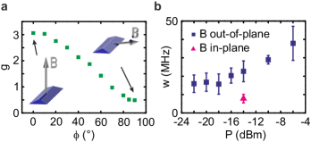
By changing the direction of the magnetic field the slope of the EDSR line is changing due to the direction dependence of the g-factor. Each of the g-factor values shown in Fig. 4a was extracted from a linear fit through several points along the respective resonance line. The g-factor values show a strong anisotropy in good agreement with earlier experimental findings for HH states24.
EDSR does not only lift PSB, but also allows the extraction of a lower limit for the hole spin dephasing time .
In order to extract a lower bound for the dephasing time the power of the applied radio frequency (RF) signal was varied. At high power, the EDSR width is power broadened. However, for measurements taken in an out-of-plane magnetic field the width is saturating at values of about -18 dBm, as can be seen in Fig. 4b.
Therefore, a lower bound for the dephasing time of about 33 ns can be extracted using the relation , where is the full width at half maximum (FWHM) of the resonance peak at a certain RF power25.
For HH states it has been predicted that the direction of the applied magnetic field has a strong influence on the dephasing times 26. Indeed, optical measurements of hole spins confined in GaAs self-assembled QDs have shown very long dephasing times 27. In order to obtain such longer dephasing times, the external magnetic field needs to be aligned perpendicular to the direction of the Overhauser field, which for HH states is perpendicular to the growth plane 26. By repeating the EDSR measurement for an in-plane magnetic field and a RF power of -14 dBm, we obtain a 68 ns dephasing time (see Supplementary Information).
In order to demonstrate coherent control over the hole spin state, periodic square pulses are applied to G1 in order to shift between the spin blockade and Coulomb blockade configuration. The modulation period is fixed to 310 ns out of which 100 ns were devoted for spin manipulation and the rest for the read-out and the initialization. The system is initialized in the triplet state. When in Coulomb blockade, a microwave burst of varying duration is applied. For a -pulse the hole spin will flip leading thus to a singlet (1,1) state. The system is then brought back into the spin blockade region for spin read-out and the hole can tunnel to the singlet (2,0) state leading to an enhanced current. By varying the duration of the microwave burst, oscillations of the detected current can be observed [Fig. 5(a)].
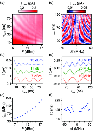
As expected, the period of the Rabi oscillations decreases with increasing power of the microwave burst [see Fig. 5(b)]. Rabi frequencies approaching 140 MHz are observed [Fig. 5(c)]. They are faster than what has been predicted for Ge nanocrystals 28 and than those reported for the InSb electron spin qubit which showed 8 ns dephasing time 29.
To measure the inhomogeneous depashing time , Ramsey experiments were performed. For this purpose, a pulse sequence consisting of two short -pulses separated by a waiting time , during which the qubit can freely evolve and dephase, was applied. For each frequency the current oscillates as a function of [Fig. 5(d)]. From the decay time of these oscillations, average dephasing times exceeding 130 ns have been measured [Figs. 5(e) and (f)]. Due to the limited visibility in our experiment, caused by the small current flowing through the DQD, it was not possible to extend the waiting time further than 160 ns. This prohibited the investigation of longer possibly arising for parallel magnetic fields as has been shown in Fig. 4(b).
In conclusion, by using PSB in a DQD device we have demonstrated the first Ge hole spin qubit with Rabi frequencies reaching 140 MHz. Despite the strong spin orbit coupling, the obtained is higher than that of holes 7 confined in QDs formed in natural Si and less than one order of magnitude lower than that of electrons 25. The reported result paves the way towards long-range two qubit-gates 30, 31.
We thank A. Hofmann, E. Laird, R. Maurand, J. Petta and M. Veldhorst for helpful discussions. This research was supported by the Scientific Service Units of IST Austria through resources provided by the MIBA Machine Shop and the nanofabrication facility. We acknowledge financial support by the Austrian Ministry of Science through the HRSM call 2016. The work was also supported by the ERC Starting Grant no. 335497, the FWF-Y 715-N30 project, the National Key R&D Program of China (Grant No. 2016YFA0301701) and the NSFC (Grants No. 11574356 and 11434010).
H.W. and J.K. contributed equally to this work.
References
- Muhonen et al. 2014 Muhonen, J. T.; Dehollain, J. P.; Laucht, A.; Hudson, F. E.; Kalra, R.; Sekiguchi, T.; Itoh, K. M.; Jamieson, D. N.; McCallum, J. C.; Dzurak, A. S.; Morello, A. Nature Nanotechnology 2014, 9, 986–991
- Jun Yoneda et al. 2017 Jun Yoneda, J.; Takeda, K.; Otsuka, T.; Nakajima, T.; Delbecq, M. R.; Allison, G.; Honda, T.; Kodera, T.; Oda, S.; Hoshi, Y.; Usami, N.; Itoh, K. M.; Tarucha, S. Nature Nanotechnology 2017,
- Vandersypen et al. 2017 Vandersypen, L. M. K.; Bluhm, H.; Clarke, J. S.; Dzurak, A. S.; Ishihara, R.; Morello, A.; Reilly, D. J.; R., S. L.; Veldhorst, M. npj Quantum Information 2017, 3
- Viennot et al. 2015 Viennot, J. J.; Dartiailh, M. C.; Cottet, A.; Kontos, T. Science 2015, 349, 408–411
- Mi et al. 2017 Mi, X.; Benito, M.; Putz, S.; Zajac, D. M.; Taylor, J. M.; Burkard, G.; Petta, J. R. arXiv:1710.03265 2017,
- Samkharadze et al. 2018 Samkharadze, N.; Zheng, G.; Kalhor, N.; Brousse, D.; Sammak, A.; Mendes, U. C.; Blais, A.; Scappucci, G.; Vandersypen, L. M. K. Science 2018,
- R. Maurand et al. 2016 R. Maurand, R.; Jehl, X.; Kotekar-Patil, D.; Corna, A.; Bohuslavskyi, H.; Laviéville, R.; Hutin, L.; Barraud, S.; Vinet, M.; Sanquer, M.; De Franceschi, S. Nature Comm. 2016, 7, 13575
- Hao et al. 2010 Hao, X.-J.; Tu, T.; Cao, G.; Zhou, C.; Li, H.-O.; Guo, G.-C.; Fung, W. Y.; Ji, Z.; Guo, G.-P.; Lu, W. Nano Lett. 2010, 10, 2956–2960
- Higginbotham et al. 2014 Higginbotham, A. P.; Larsen, T. W.; Yao, J.; Yan, H.; Lieber, C. M.; Marcus, C. M.; Kuemmeth, F. Nano Lett. 2014, 14, 3582–3586
- Kloeffel et al. 2017 Kloeffel, C.; Rančić, M. J.; Loss, D. arXiv:1712.03476 2017,
- Marcellina et al. 2017 Marcellina, E.; Hamilton, A. R.; Winkler, R.; Culcer, D. Phys. Rev. B 2017, 95, 075305
- Xiang et al. 2006 Xiang, J.; Vidan, A.; Tinkham, M.; Westervelt, R. M.; Lieber, C. M. Nature Nanotechnology 2006, 1, 208–213
- Katsaros et al. 2010 Katsaros, G.; Spathis, P.; Stoffel, M.; Fournel, F.; Mongillo, M.; Bouchiat, V.; Lefloch, F.; Rastelli, A.; Schmidt, O. G.; De Franceschi, S. Nature Nanotechnology 2010, 5, 458–464
- N. W. Hendrickx et al. 2018 N. W. Hendrickx, N. W.; Franke, D. P.; Sammak, A.; Kouwenhoven, M.; Sabbagh, D.; Yeoh, L.; Li, R.; Tagliaferri, M.; Virgilio, M.; Capellini, G.; Scappucci, G.; Veldhorst, M. arXiv:1801.08869 2018,
- Hu et al. 2012 Hu, Y. J.; Kuemmeth, F.; Lieber, C. M.; Marcus, C. M. Nature Nanotechnology 2012, 7, 47–50
- Brauns et al. 2016 Brauns, M.; Ridderbos, J.; Li, A.; Bakkers, E. P. A. M.; Zwanenburg, F. A. Phys. Rev. B 2016, 93, 121408(R)
- Hu et al. 2007 Hu, Y. J.; Churchill, H. O. H.; Reilly, D. J.; Xiang, J.; Lieber, C. M.; Marcus, C. M. Nature Nanotechnology 2007, 2, 622–625
- Zhang et al. 2012 Zhang, J. J.; Katsaros, G.; Montalenti, F.; Scopece, D.; Rezaev, R. O.; Mickel, C.; Rellinghaus, B.; Miglio, L.; De Franceschi, S.; Rastelli, A.; Schmidt, O. G. Phys. Rev. Lett. 2012, 109, 085502
- Watzinger et al. 2014 Watzinger, H.; Glaser, M.; Zhang, J. J.; Daruka, I.; Schäffler, F. APL Mater. 2014, 2, 076102
- Ono et al. 2002 Ono, K.; Austing, D. G.; Tokura, Y.; Tarucha, S. Science 2002, 297, 1313–1317
- van der Wiel et al. 2002 van der Wiel, W. G.; De Franceschi, S.; Elzerman, J. M.; Fujisawa, T.; Tarucha, S.; Kouwenhoven, L. P. Rev. Mod. Phys. 2002, 75
- Hanson et al. 2007 Hanson, R.; Kouwenhoven, L. P.; Petta, J. R.; Tarucha, S.; Vandersypen, L. M. K. Rev. Mod. Phys. 2007, 79, 1217–1265
- Golovach et al. 2006 Golovach, V. N.; Borhani, M.; Loss, D. Phys. Rev. B 2006, 74, 165319
- Watzinger et al. 2016 Watzinger, H.; Kloeffel, C.; Vukušić, L.; Rossell, M. D.; Sessi, V.; Kukučka, J.; Kirchschlager, R.; Lausecker, E.; Truhlar, A.; Glaser, M.; Rastelli, A.; Fuhrer, A.; Loss, D.; Katsaros, G. Nano Lett. 2016, 16, 6879–6885
- Kawakami et al. 2014 Kawakami, E.; Scarlino, P.; Ward, D. R.; Braakman, F. R.; Savage, D. E.; Lagally, M. G.; Friesen, M.; Coppersmith, S. N.; Eriksson, M. A.; Vandersypen, L. M. K. Nature Nanotechnology 2014, 9, 666–670
- Fischer et al. 2008 Fischer, J.; Coish, W. A.; Bulaev, D. V.; Loss, D. Phys. Rev. B 2008, 78, 155329
- Prechtel et al. 2016 Prechtel, J. H.; Kuhlmann, A. V.; Houel, J.; Ludwig, A.; Valentin, S. R.; Wieck, A. D.; Warburton, R. J. Nature Mat. 2016, 15, 981–986
- Ares et al. 2013 Ares, N.; Katsaros, G.; Golovach, V. N.; Zhang, J. J.; Prager, A.; Glazman, L. I.; Schmidt, O. G.; De Franceschi, S. Appl. Phys. Lett. 2013, 103, 263113
- van den Berg et al. 2013 van den Berg, J. W. G.; Nadj-Perge, S.; Pribiag, V. S.; Plissard, S. R.; Bakkers, E. P. A. M.; Frolov, S. M.; Kouwenhoven, L. P. Phys. Rev. Lett. 2013, 1110, 066806
- Nigg et al. 2017 Nigg, S. E.; Fuhrer, A.; Loss, D. Phys. Rev. Lett. 2017, 118, 147701
- Kloeffel et al. 2013 Kloeffel, C.; Trif, M.; Stano, P.; Loss, D. Phys. Rev. B 2013, 88, 241405(R)