Non-scattering Metasurface-bound Cavities for Field Localization, Enhancement, and Suppression
Abstract
We propose and analyse metasurface-bound invisible (non-scattering) partially open cavities where the inside field distribution can be engineered. It is demonstrated both theoretically and experimentally that the cavities exhibit unidirectional invisibility at the operating frequency with enhanced or suppressed field at different positions inside the cavity volume. Several examples of applications of the designed cavities are proposed and analyzed, in particular, cloaking sensors and obstacles, enhancement of emission, and “invisible waveguides”. The non-scattering mode excited in the proposed cavity is driven by the incident wave and resembles an ideal bound state in the continuum of electromagnetic frequency spectrum. In contrast to known bound states in the continuum, the mode can stay localized in the cavity infinitely long, provided that the incident wave illuminates the cavity.
Index Terms:
Bound states, metasurface, cloaking, driven bound states, field localization, invisible resonators, zero-phase transmissionI Introduction
Localization of electromagnetic waves plays central role for applications in various fields of technology such as lasers, filters, optical fibers, nonlinear devices. Especially in nanophotonics achieving high field concentration in optically compact systems is of paramount importance [1, 2]. A simple example of wave localization is the echo inside a cave. Sound waves created by an object inside the cave cannot escape outside and experience multiple reflections from its hard walls before getting eventually absorbed. Meanwhile, the strength of sound can be strongly amplified in this cavity due to the wave interference. However, waves which excite a resonant mode from outside are weakly coupled to the cavity and are mostly reflected back to the external space. Therefore, a pertinent question arises whether it is possible to localize waves in a space region without isolating it by walls and, most importantly, without disturbing the waves incoming into it from outside. Such space region would appear for an external observer as free space (fully imperceivable), while it would operate as a resonant cavity for an observer inside it.
An apparent solution for realizing strong field localization in an open system is based on Fabry-Perot interferometers [3, 4, 5] formed by two partially transparent mirrors separated by a specific distance. At discrete wavelengths, lossless Fabry-Perot resonators pass through all the power carried by the incident waves due to the destructive interference of reflected waves between the mirrors. However, these resonators are still perceivable for an external observer since they alter the phase of the transmitted waves, that is, they produce scattered waves. This forward scattering represents little-or-no inconvenience for applications that require unitary power transmission. However, performance of synchronous systems, such as array beamformers [6], homodyne interferometry [7], and high-resolution astronomical observations [8], is degraded drastically in the presence of forward scattering. Hence, solution for latter scenarios requires open non-scattering cavities which the field outside of the cavity is not modified at all. Furthermore, studies of non-scattering resonant objects are of fundamental interest as realizations of bound eigenstates in the continuum.
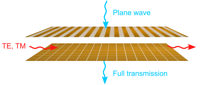
Theory of non-scattering and non-radiating bodies has a long history dating back to the work by Ehrenfest, where he recognized that radiationless current distributions are possible [9, 10, 11, 12], being the starting point for new and innovative concepts and applications [13]. Nevertheless, such systems do not necessary allow one to achieve strong fields localizations. For example, consider a non-scattering configuration which includes two planar metasurfaces [14, 15]: Each sheet does not produce back scattering, while in the forward direction their scattering can be mutually compensated. As a result, the field between the interfaces is identical to that of the incident wave and cannot reach extreme values.
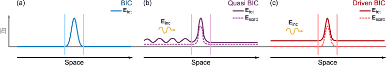
Thus, realization of invisible cavities implies combination of field enhancement properties of Fabry-Perot resonators and invisibility features of non-scattering electromagnetic systems. This scenario to some extent resembles bound states in the continuous spectrum of frequencies (BICs), i.e. non-radiating eigenmodes captured into a localized volume [16] [see Fig. 1(a)]. First studies of this concept were made by von Neumann and Wigner [17, 18] in quantum mechanics, and expanded through the years to other branches of physics: photonics [19, 20, 21, 22, 23, 24, 25, 26, 27, 28, 29, 30, 31, 32, 33], acoustics [34, 35], electronics [36, 37], and others [38]. Ideal BICs, with an infinite quality factor, cannot be excited from outside and are practically impossible due to dissipation loss present in all physical systems. Instead, it is more relevant to speak about quasi BICs, with a large but finite lifetime, which are feasible under realistic conditions [see Fig. 1(b)]. A quasi BIC, in the absence of incident waves, slowly leaks the stored energy away from the localization region. Due to that, an external incident wave is used to extend the lifetime of the eigenmode, compensating the leaked energy. In the best scenario, back scattering is eliminated but forward scattering shifts the phase of the transmitted wave. In contrast to quasi BIC, the eigenmode excited inside invisible resonators which we introduce and study here [see Fig. 1(c)] does not decay and at the same time does not scatter under the presence of an incident wave. In fact, the scattering profile of an invisible resonator resembles the field distribution of an ideal BIC [compare the dashed line of Fig. 1(c) with BIC profile of Fig. 1(a)], resulting in a cavity eigenmode “driven” by the incident wave. Their distinctive features make invisible cavities good candidates for various applications, while practical implementation of quasi BICs have been scarce to date and limited to very recent works [39, 40, 41].
In this paper, we propose and design invisible cavities formed by two parallel thin patterned metal sheets (1D scenario). We call the sheets planar metasurfaces [42, 43] (or frequency-selective surfaces in special cases [44]). We demonstrate, both numerically and experimentally, unidirectional invisibility of the cavity at the operating frequency with localized field enhancement and suppression at different positions between the metasurfaces. The amplitude of the field within the cavity depends on the degree of transparency of the metasurfaces, and, in the limiting case, the non-scattering modes (so-called driven BICs) converge to ideal BICs. Several examples of applications of the designed invisible cavities are proposed and analyzed, in particular, cloaking sensors and obstacles. Furthermore, we demonstrate that in the extreme reactances limit, the proposed cavities exhibit essentially different convergence to the ideal BICs as compared to conventional cavities, providing an efficient route towards realizations of finite-time excitation of BICs with theoretically infinite lifetime.
II Design of invisible cavities
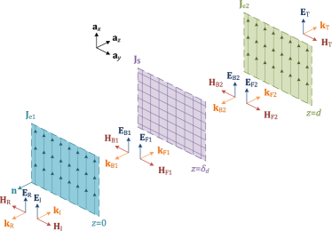
Let us consider a one-dimensional scenario, where two metasurfaces infinite in the plane are separated by a distance in a homogeneous medium (assumed to be vacuum in this work), as shown in Fig. 2. The metasurfaces represent artificial composite sheets: subwavelength periodic structures with negligible thickness, designed for electromagnetic wave manipulations [42, 43]. When such a cavity is excited by a normally incident plane wave, electric currents (characterized by the surface current densities and ) are excited in the metasurfaces, which produce scattered waves inside and outside the cavity. Each metasurface is characterized by its grid impedance ( and , respectively), defined as the ratio of the tangential component of the surface-averaged electric field at the metasurface position and the induced electric current density.
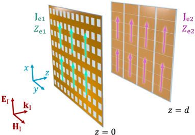
We design the cavity so that it produces no scattered waves outside it, meaning that the reflected wave should be eliminated () and the transmitted wave should be equal to the incident wave () without any phase lag. Field solutions on the base of the impedance boundary conditions at both sheets (see Appendix A) lead us to the following conditions on the grid impedances and the distance :
| (1) |
We see that the cavity is invisible only when the distance between the metasurfaces is fixed to an integer of the half-wavelength of the supporting medium. On the other hand, the metasurfaces can have arbitrary complex grid impedances as long as the two values satisfy Eqs. (1).
This relation between the grid impedances implies that if one metasurface is lossy, then the second one should be pumped with external energy to compensate the power dissipated in the lossy sheet. In the limiting case of active/lossy metasurface combination, when the impedances and are purely real, the cavity behaves as a teleportation slab with parity-time symmetry [45]. However, for practical implementations of the structure, it is desirable to use purely imaginary grid impedances (using easily realizable capacitive and inductive metasurfaces), which is the case when dissipation is negligible (influence of inevitable small losses on the cavity performance is elucidated below).
While the scattering from such invisible cavities is completely suppressed, the fields inside it are different from the incident field and can be found as combinations of forward and backward propagating waves. This solution corresponds to the homogenized impedance model of metasurfaces, which is valid when the distance between the sheets is considerably larger than the metasurface array period (so that the evanescent waves excited due to the discrete structure of the metasurface decay to negligible level). In this case, the field inside the cavity can be modelled as a standing wave (see derivations in Appendix B).
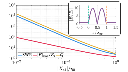
Therefore, the ratio between the maximum and minimum values of the electric field magnitude inside the cavity can be characterized by the standing wave ratio (SWR), which is defined for the invisible cavity as
| (2) |
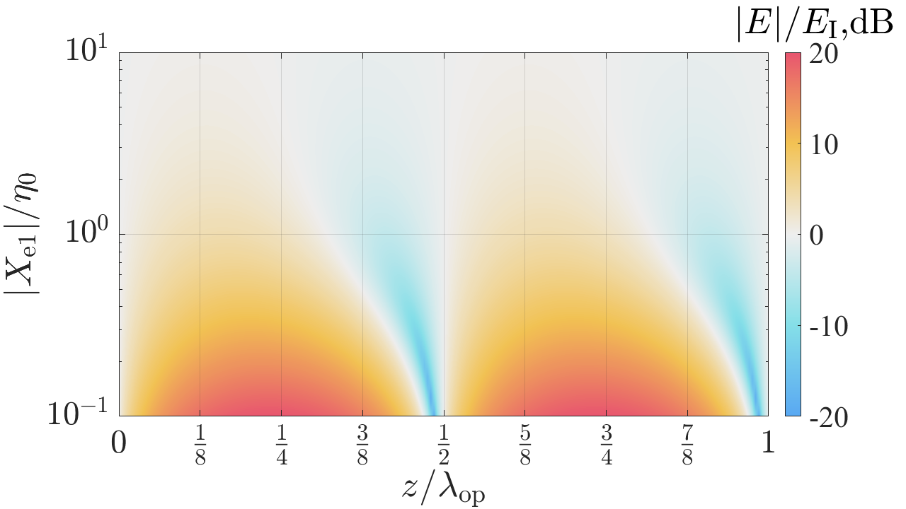
Figure 3 illustrates the dependence of the standing wave ratio for lossless invisible cavities versus the grid reactance. Notice that SWR increases as both grid impedances converge to zero. This is important as highly localized fields are achieved with metasurfaces whose properties are close to those of a continuous sheet of perfect electric conductor (PEC).
Another useful characteristic of cavity properties is the quality factor , which measured the relative bandwidth of the transmission window: . By defining the relative bandwidth by the half-power level, we obtain the following expression for a lossless invisible cavity with near-PEC metasurfaces (see derivation in Appendix B):
| (3) |
The quality factor grows to infinity when the grid impedances tend to zero (the PEC limit) approximately as , and it is also directly proportional to the distance between the metasurfaces (represented by the integer ). Thus, maximization of the quality factor, desired for many applications, is achieved when the cavity thickness is large and the grid impedance is small, as shown in Fig. 3. It should be noted that this definition of the quality factor implies lossless and dispersionless unit cells of the metasurfaces (additional frequency dispersion of lossless metasurfaces generally results in increasing the quality factor due to additional storage of reactive energy).
III Driven bound states in the continuum
As it was mentioned above, for finite values of the sheet reactances the non-scattering eigenmode (eigenstate) of invisible metasurface-bound cavities is a driven bound state in the continuous spectrum of frequencies, in contrast to full-transmittance modes of conventional Fabry-Perot resonators. At the frequency of the mode, the scattered field is completely localized inside the cavity [the cavity appears invisible as is illustrated in Fig. 1(c)], while at all higher and lower frequencies the cavity produces scattered fields, yielding a continuous spectrum of unbounded states. The name “driven” comes from the fact that this bound state does not leak energy only when the cavity is illuminated by a plane wave. If the illumination is switched off, the excited mode energy will eventually leak away.
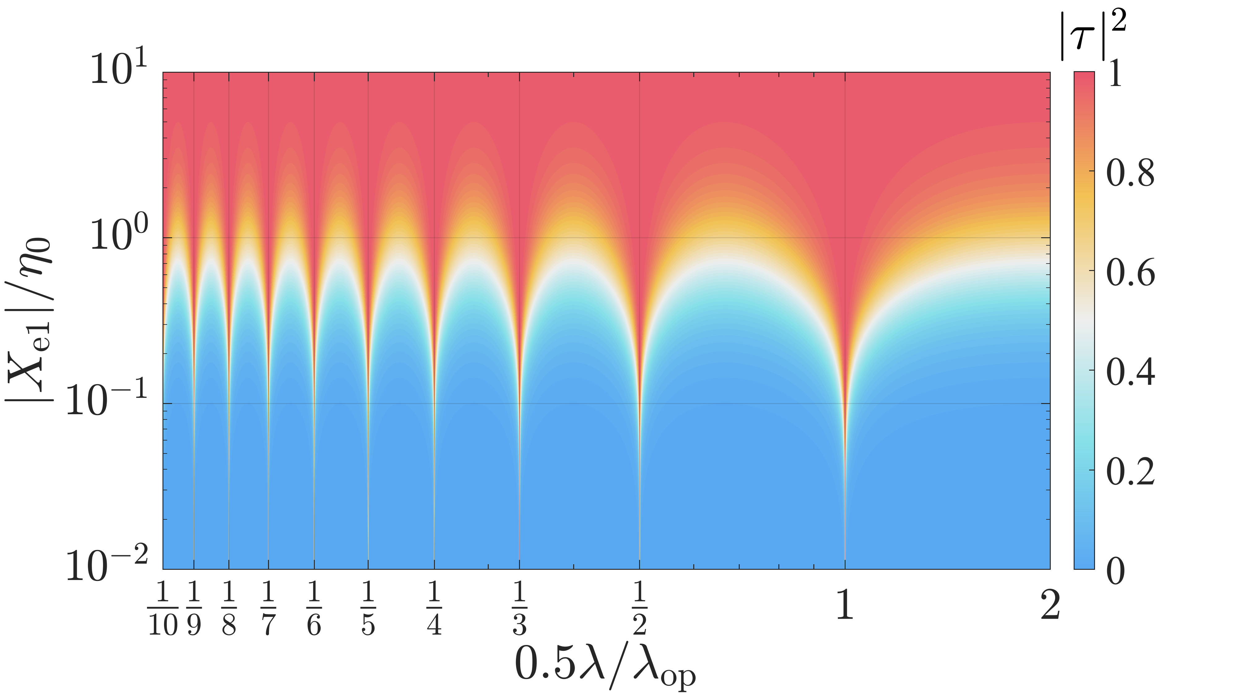
A distinctive feature of driven BICs is that they have infinite lifetime (limited only by duration of the external illumination) in cavities with a finite Q-factor. According to Fig. 3, as the grid impedances of the metasurfaces approach zero, the Q-factor tends to infinity, and the driven eigenmode becomes an ideal BIC. Figure 4 shows the transmittance through the cavity as a function of the metasurface grid reactance and the wavelength of incident waves . One can clearly recognize sharp resonances of the cavity at ( is a positive integer) corresponding in the limit of to ideal BICs.
Interestingly, in the limit of and , both metasurfaces become identical. Nevertheless, it is important that the grid reactances and tend to zero from the opposite sides so that condition holds. Figure 5(a) shows reflectance and transmittance through the cavity for two convergence scenarios: When and when .
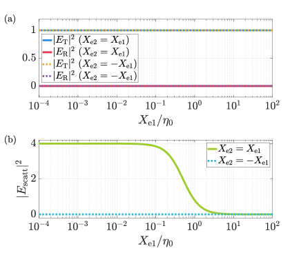
In the former case, the cavity is invisible for all reactance pairs; while in the latter case, the FP-based cavity remains transparent everywhere. To quantify the degree of invisibility we plot the difference between the transmitted and the incident wave amplitudes, on Fig. 5(b). The dramatic difference of the two curves is evident. We see that the Fabry-Perot cavity formed by two identical metasurfaces becomes invisible only in the trivial limit of infinite sheet reactances (no metasurfaces at all). For moderate and small values of the sheet reactance, scattering is strong although the power transmittance tends to unity for small reactances. Thus, while invisible cavities do not scatter at all, Fabry-Perot resonators produce a strong forward scattered wave that, combined with the incident wave, results in a phase shift of the transmitted wave.
IV Realization of invisible cavities
In order to verify the theoretically predicted behavior of invisible cavities, a set of waveguide experiments was carried out. It is well known that the fundamental TE10 mode propagating in a waveguide with the rectangular cross-section of the dimensions with electric field magnitude and the wavenumber can be described as a superposition of two TEM plane waves as follows:
| (4) |
In the last expression is the frequency-dependent angle of incidence of the plane waves with respect to the -axis of the waveguide and is their magnitude. Therefore, the problem of scattering of the fundamental mode by a thin obstacle placed in the cross-section of the waveguide is electromagnetically equivalent to that of plane-wave scattering by a periodic array of such obstacles with the periodicities and along the and axes, respectively. Although this method does not provide an arbitrary choice of the incidence angle at the operational frequency and does not support normal incidence, it is still applicable to analyze the proposed invisible cavities. As the wavelength of the TE10 mode equal to differs from the wavelength in free space, in our approach the separation of metasurfaces in the cavity (multiple of half-wavelengths) should be modified accordingly. It is, however, possible to demonstrate that the requirement of mutually complex-conjugate grid impedances still holds for the metasurfaces providing theoretically perfect non-scattering regime in the case of oblique incidence.
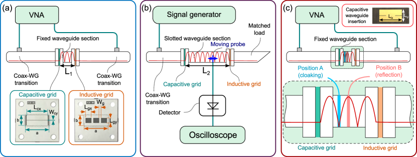
To reach the non-scattering regime, both the capacitive and inductive metasurfaces, represented by their single rectangular unit-cells, were numerically optimized to provide the grid impedance of . The capacitive metasurface unit cell comprised a rectangular copper patch of the length mm and height mm (here mm is the gap width) printed on a 0.5-mm-thick Arlon AD250 substrate with the relative permittivity of 2.5 and the dielectric loss tangent 0.0018 [see illustration in Fig. 6(a)]. To ensure the grid impedance of at GHz, the width of the gap between adjacent patches in the corresponding periodic metasurface was parametrically tuned to 0.3 mm. The unit cell of the inductive metasurface was represented by three rectangular apertures of the dimensions mm2 each separated by copper strips of the widths mm printed on a similar substrate. The latter value was chosen to provide the required value of the grid impedance of . The parameters of for the capacitive unit cell and for the inductive one were determined separately by placing the corresponding structure into a waveguide section terminated by two waveguide ports and extracting the grid impedances from measured reflection and transmission coefficients. Due to the losses in the copper metallization and the substrates, both grid impedances have a small real part. The extracted impedance for the capacitive grid was and for the inductive one. These real parts of the grid impedances were taken into account when comparing the experimental results with numerical data (consider information provided in Appendix C).
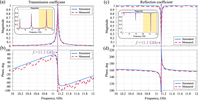
The aim of the first experiment was to demonstrate the operation of the invisible cavity or, in other words, to show that properly choosing the properties of the metasurfaces, high transmission at the resonance is achieved along with zero transmission phase. In the waveguide setup, each of the two unit cells was surrounded with a continuous metalized area on both layers of the PCB with multiple vias at the periphery of the waveguide cross-section to ensure no current discontinuity on the waveguide walls. The photographs of the manufactured unit cells to be inserted before and after the waveguide section are shown in insets of Fig. 6(a). The distance between them is three half-wavelengths, i.e. . The complex transmission and reflection coefficients were retrieved from S-parameters measured by a vector network analyzer (VNA) using additional calibration data corresponding to an empty waveguide and a metal plate connected to the waveguide instead of each metasurface unit cell. The experimental setup used for characterization of the reflection and transmission coefficients of the invisible cavity is schematically shown in Fig. 6(a). It is based on a uniform WG-90 waveguide section fixed between two coax-to-waveguide transitions from Agilent X11644A WR-90 X-band kit connected to ports of a vector network analyzer Agilent E8362C. The length of the section was equal to mm, which for the waveguide cross-section of mm2 resulted in the third thickness resonance condition at GHz. In other words, equals to three half-wavelengths in the waveguide at , while the wavelength equals to mm.
Figure 7 shows the measured transmission (left) and reflection (right) coefficients through the cavity in the frequency range from to GHz. The insets show the same parameters but in the extended frequency range from to GHz. As one can see from the plots, there are three separate thickness resonances in the extended range. At each resonant frequency, the transmission coefficient magnitude is high, however it exceeds 0.9 only at the third resonance ( GHz), i.e. at the frequency where the impedances of the inserted metasurfaces were designed to be complex conjugate of each other. The experimentally achieved transmission coefficient magnitude at the maximum was instead of predicted by the simulation due to some misalignment of the capacitive and inductive unit cells with respect to the cross-section plane. These results are in good agreement with theoretical predictions for lossy metasurfaces (see Appendix C). Indeed, the theoretical data provide estimated transmission coefficient of and nearly zero reflection coefficient for the designed metasurfaces with . Furthermore, as one can check from the measured phase plots in Fig. 7(b), the transmission coefficient phase crosses zero at the same resonance frequency. The measured quality factor is . Therefore, it is experimentally confirmed that the cavity is indeed practically invisible (non-scattering) for the chosen excitation. The experimental curves are in good correspondence with numerically calculated ones.
Next, to demonstrate the effect of resonant field enhancement in the invisible cavity, the same manufactured unit cells were employed, but the uniform section was replaced with another, three times longer calibrated measurement waveguide section P1-20 with the length mm, as shown in Fig. 6(b). The latter had a longitudinal thin slot in the middle of the broad side of the waveguide and was equipped with a movable thin-wire probe to measure the electric field distribution with minimum insertion and reflection losses. The probe was connected to the digital oscilloscope Rohde & Schwarz HMO2022 through a diode detector. The waveguide was fed from one side by connecting the signal generator Rohde & Schwarz SMB100A, while loaded with a matched load from the other side. The generator produced a wave at the carrier frequency of GHz modulated with a harmonic signal with the frequency of kHz. The probe was mechanically moved to plot the electric field magnitude versus the longitudinal coordinate by checking the amplitude of the detected signal at the modulation frequency and applying the calibration characteristic of the detector. Normalized to the field magnitude in the waveguide section without the cavity, the field can be determined quantitatively.
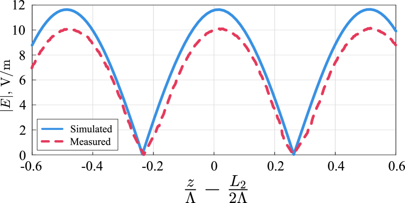
For comparison, the realized metasurface unit cells were numerically simulated inside a waveguide section and the calculated field patterns were compared with the measured ones. The measured and simulated electric field distributions at the resonant frequency of GHz are compared in Fig. 8, where the field in the empty waveguide was taken as V/m. Due to the physical constrains related with the slotted waveguide probe, only one third of the invisible cavity was characterized, as shown in Fig. 8 for the coordinate range from to mm.
The measured field profile is in good agreement with the simulated one. The difference of the measured resonant field enhancement from the numerically predicted value (10 versus ) can be explained by radiation leakage losses due to the measurement slot and the probe effect. Therefore, it was observed that the designed non-scattering cavity at GHz causes an order-of-magnitude field enhancement and suppression. Likewise, these results are in good agreement with theoretical predictions for lossy metasurfaces (see Appendix C under the assumption of ).
V Applications of invisible cavities
Manipulation of scattering from an object placed inside the cavity
As was discussed above, the proposed cavities provide enhancement and suppression of fields inside, keeping the fields outside undisturbed. Such functionality provides unique opportunities for manipulating scattered fields from objects placed inside the cavity. Indeed, placing an object in the field minima (maxima), one can suppress (enhance) wave scattering from it since the local field at the object position is decreased (increased) compared to the incident field. The best effect is achieved when the object is planar (since we consider 1D invisible cavities).
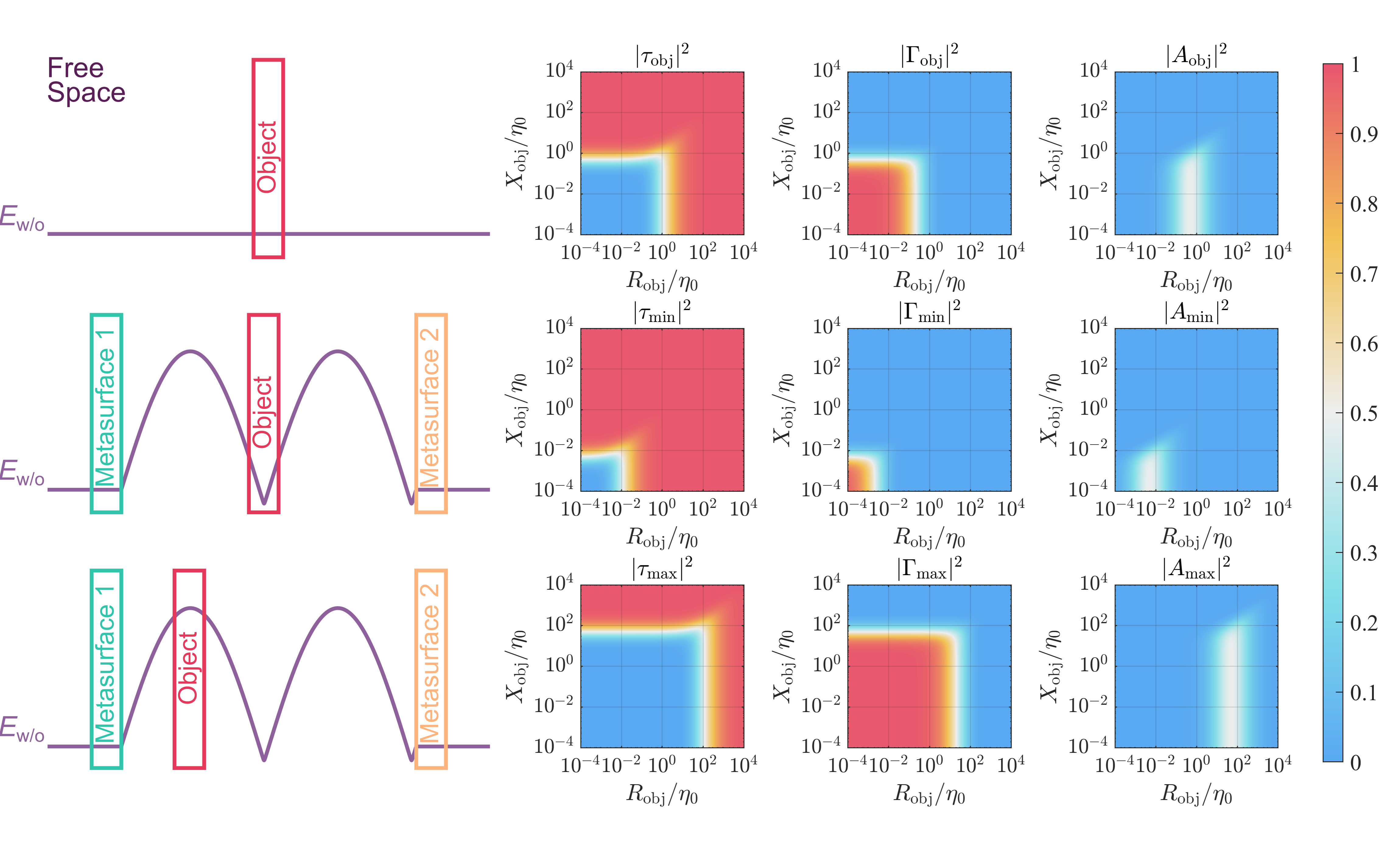
We model the object whose scattering should be enhanced or suppressed as a thin sheet with the grid impedance (only electric polarization response is assumed). Positioning the object at a distance , we can determine reflected and transmitted fields from it in the presence and absence of the cavity (see Appendix D). Figure 9 shows the reflectance, transmittance, and absorbance of incident waves in three scenarios: When the object is in free space (without the cavity), and when it is placed in the field maximum and minimum inside the cavity (here, we chose ).
Comparison of the plots in the first and second rows (free-space and field-minimum scenarios) reveals that by positioning an arbitrary object at the field minimum of the cavity, one can drastically decrease reflection from the object. Absorption can be decreased or increased depending on the grid impedance of the object. The transmittance in this case is more than when . The phase of transmission is close to zero, which implies strongly suppressed scattering from the object (note that the object alone transmits less than 3% when ). Thus, the invisible cavity can be exploited for scattering suppression from planar layers. The smaller grid reactances of the metasurfaces, the greater suppression effect can be achieved (higher Q-factor). On the contrary, the smaller grid impedance of the object to be hidden, the lower the effect. In the limit of the object made from perfect electric conductor, full reflection occurs even in the presence of the cavity. By comparing the first and third rows in Fig. 9 (the free-space and field-maximum scenarios), one can see that depending on the grid impedance of the object, the cavity can increase (up to 50%) or decrease absorption in the object. At the same time, reflection is always increased and transmission decreased. Such functionality can be used for enhancement of the energy captured by sensors.
To verify these results, we carried out the third experiment, where we measured scattering from a planar object (with a given grid impedance) placed either at the minimum [Position A indicated in Fig. 6(c)] or at the maximum [Position B] of the electric field distribution inside the cavity. To test scattering enhancement/suppresion, we used the same capacitive and inductive grids as shown in Fig. 6(a) to form the cavity. The planar object was also made as a printed circuit board with a carefully designed copper shape printed on one side of Arlon AD250 0.5-mm-thick substrate. However, to place the object into an arbitrary position in the previously used uniform section, the dimensions of the board were chosen almost equal to those of the waveguide cross section. At the same time, the metal pattern was designed to provide the grid impedance of at GHz with no electric contact to the waveguide walls required. The photograph of the object and the scheme of its insertion into the waveguide are illustrated on the insets in Fig. 6(c). The shape was a rectangular patch of the dimensions mm2, in which two symmetrical notches of the width of mm and the length of mm were made to reach the desired grid capacitance. To fix the object inside the waveguide, thin foam holders were employed.
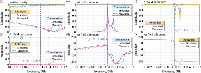
As can be seen in Fig. 10(a), the low grid capacitance of the object leads to high reflection ( at GHz) in the absence of the cavity. However, when the same object is placed in the electric field maximum inside the invisible cavity, the reflection coefficient becomes very close to unity in the whole frequency range from to GHz [as shown in Fig. 10(b)]. Therefore, in this case one observes broadband enhancement of reflectivity or scattering from an object placed inside the cavity.
On the contrary, when the object is placed in the minimum of the electric field distribution inside the cavity, the simulated and measured transmission and reflection coefficients shown in Fig. 10(c-f) look drastically different. Indeed, as is seen from Fig. 10(c), the measured transmission coefficient magnitude reaches at the resonance frequency of the cavity ( GHz) despite that the inserted metasurface itself was highly reflective. Interestingly, the transmission coefficient phase is still zero at this frequency. The experimentally achieved transmission coefficient magnitude of differs from the simulated value of due to small misalignments of the capacitive and inductive unit cells as well as the object with respect to the cross-section plane. Nevertheless, it is possible to conclude that when the reflective metasurface is properly inserted into the invisible cavity, scattering is nearly totally suppressed (some residue scattering occurs due to absorption in metal parts). The other noticeable effect is the second resonance appeared at 11.32 GHz, which can be explained by the fact that the object paired with the capacitive metasurface of the cavity forms a new Fabry-Perot cavity. In this new cavity both walls have the same reactance of , so this new cavity is not transparent, as one can observe from the transmission and reflection magnitudes at GHz in Fig. 10(c,e). Moreover, because of its Fabry-Perot nature, this new cavity does not provide zero transmission phase at its resonance frequency as can be clearly seen from Fig. 10(d).
The above mentioned method to manipulate scattering is applicable for thin sheets with arbitrary grid impedances. However, if the object impedance is known, scattering can be suppressed by cascading the object and one metasurface (with the opposite grid impedance). In this way, the object plays the role of the second metasurface in an invisible cavity and the total scattering from this system becomes zero.
Transparent waveguides
An invisible resonator made of high-reflective metasurfaces illuminated at normal incidence ensures field localization without scattering. On the other hand, a wave propagating parallel to the metasurfaces can be also localized between them, like in a parallel-plate waveguide [46]. To consider this property, we studied guided modes which can propagate between the metasurfaces for the same structure as studied above. At the frequency GHz, at which the transmission coefficient is unity for normal incidence (assuming , ), it is simultaneously possible to excite two different modes at the input port of the waveguide, as shown in Fig. 11: a transverse electric mode TE (whose longitudinal component of electric field is zero) and a transverse magnetic mode TM (whose longitudinal component of magnetic field is zero), respectively.
For both modes, the energy is confined inside the cavity and exponentially decays in free space outside the cavity. However, the attenuation constant is quite different for the two modes. The TE mode has a higher attenuation constant ( m-1) compared to the TM mode ( m-1). Knowing the attenuation constants, we can find the distance away from the metasurface at which the field reaches of its magnitude at the metasurface boundary. For the TE mode mm, while mm for the TM mode (less than 1/12 of the wavelength). It is worth noting that the phase and attenuation constants remain unchanged for different distances between metasurfaces.
Multi-layer resonators
An intuitive method to achieve even higher field localization is inserting an open cavity resonator inside another one [as shown in Fig. 12(a)], such that the standing wave inside the inner cavity is fed by the outer resonator standing wave. Stacking open cavities which produce non-zero scattering, such as conventional Fabry-Perot resonators, is possible but not intuitive since it requires careful design of both cavities taking into account complex interference between them [47]. However, if one utilizes the invisible cavities proposed in this paper, the design becomes straightforward. Indeed, since the inner cavity generates no external scattering, the standing wave in the outer cavity is not affected by it. Furthermore, the zero-scattering property of the combined structure is granted regardless of the inner cavity position.
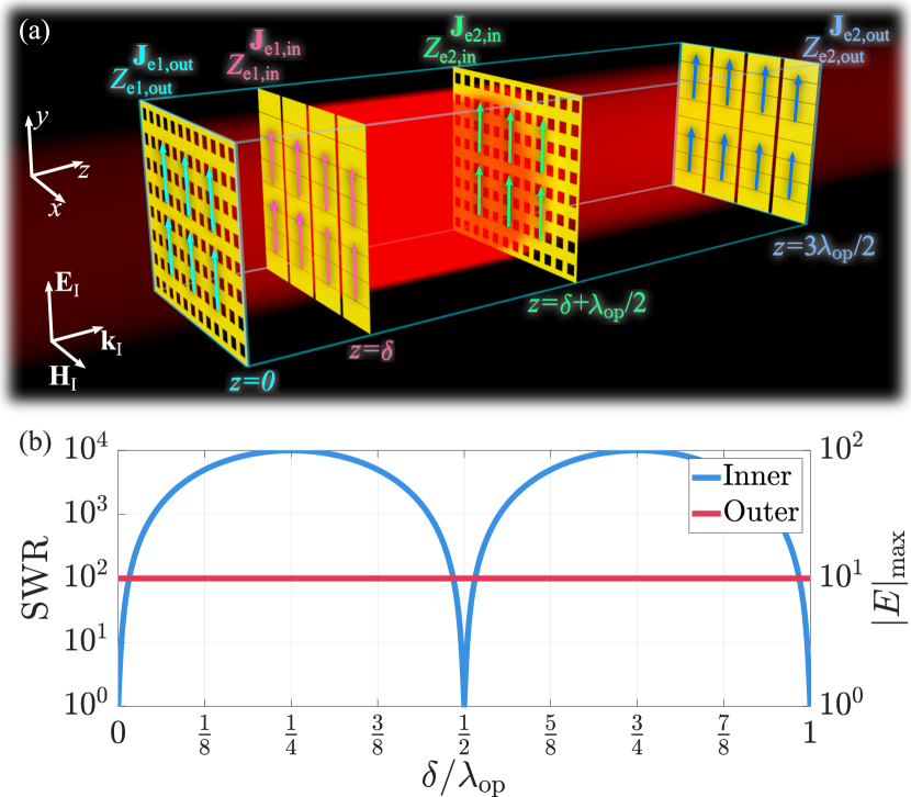
This peculiar combination of cavities, resembling a “matryoshka” doll, makes the displacement of the inner resonator an additional degree of freedom which can be exploited to achieve giant field enhancement inside the cavity and high SWR. The scattered fields across the structure can be found solving similar electromagnetic problems as done before for a single resonator [see Eqs. (7) in Appendix A], by just adding two more metasurfaces at and and considering the inner and outer pairs as invisible resonators [using conditions of Eqs. (1)]. In the case that the multi-layer resonator is composed by alternating grid impedances , the standing wave can be defined by its inner forward and backward components:
| (5a) | ||||
| (5b) | ||||
| (5c) | ||||
These expression for SWR can be obtained using Eqs. (11) and (12) of Appendix B.
Figure 12(b) demonstrates that by adjusting the distance , SWR and the maximal of electric field can be enhanced reaching the square values of those corresponding to a single cavity with given grid reactance (in this example we consider metasurfaces with grid impedance ). On the other hand, the inner resonator can be positioned in such a way that there is no field enhancement at all. This invisible multi-layer configuration can be easily extended to any multiple of stacked cavities, which makes it very appealing for applications where high localization and field enhancement are required.
VI Discussion
In this work, we have proposed and designed one-dimensional cavities which are imperceivable (non-scattering) for an external observer while still provide strong field localization inside their volumes. The non-scattering regime occurs in a cavity formed by two metasurfaces due to destructive interference of waves scattered by each metasurface. In the former case, the distance between metasurfaces must be equal to an integer of half-wavelengths, while their grid impedances must have the opposite signs. The non-scattering mode excited in such a cavity is driven by the incident wave and resembles an ideal bound state in the continuum of electromagnetic frequency spectrum. In contrast to known bound states in the continuum, the mode can stay localized in the cavity infinitely long without scattering, provided that the incident wave illuminates it. In the limit of zero reactances of the two sheets, the resonant mode converges to an ideal embedded eigenstate in the continuum.
Although the described theory analyzes a one-dimensional scenario of invisible cavities, it can be extended in a similar way to the two- and three-dimensional scenarios. In fact, with appropriate modifications, the fabricated cavity was proved to be functional inside a rectangular waveguide, preserving all its unique properties. With the proper positioning of a thin planar object inside the cavity, one can increase or reduce electromagnetic scattering from it, with the potential applications in cloaking and sensing. Moreover, the proposed structures can be used to guide transverse electromagnetic waves along them, remaining invisible for normally incident radiation (invisible parallel-plate waveguides). Due to the reciprocity of the structure, the cavity offers new possibilities for emission control of active sources located inside it.
Appendix A:
Solution of the boundary problem and conditions for the required grid impedances
Consider the scenario illustrated in Fig. 2, where two metasurfaces are separated by a distance . Under normal plane-wave illumination by an incident wave with electric field , the metasurfaces create secondary electromagnetic plane waves. The reflected (“R”) and transmitted (“T”) waves propagate in the and regions, respectively. Meanwhile, a standing wave inside the cavity can be described as a superposition of forward (“F”) and backward (“B”) waves. The electric fields of these plane waves read
| (6a) | ||||
| (6b) | ||||
| (6c) | ||||
| (6d) | ||||
| (6e) | ||||
where and are the wavenumber and the characteristic impedance of the medium (assumed to be vacuum for simplicity).
Let us write the generalized sheet transition conditions for each metasurface:
| (7a) | ||||
| (7b) | ||||
| (7c) | ||||
| (7d) | ||||
where and are the electric surface current densities at each metasurface, respectively. The current density satisfies impedance boundary conditions, where the grid impedance is defined by the geometry and properties of the unit cells and the array period. In our scenario, substituting the expressions for the electric fields, the impedance relations take the form
| (8a) | ||||
| (8b) | ||||
The magnitude of each plane wave can be determined as a function of the grid impedances, the electric properties of the propagating medium, and the distance between the metasurfaces:
| (9a) | ||||
| (9b) | ||||
| (9c) | ||||
| (9d) | ||||
| (9e) | ||||
Requiring the absence of scattering in Eqs. (9) ( and ), the conditions of Eqs. (1) are met.
Appendix B:
Properties of Invisible Cavities
Fields inside the cavity and the standing-wave ratio
Plane waves created by metasurface currents can form a standing wave between them. The total internal electric field is the sum of the forward wave and the backward wave :
| (10) |
Figure 13 illustrates the electric field strength at different locations inside a lossless cavity (, ) as a function of the reactance value . As is typical for standing waves, it is seen that the field distribution has a repeating pattern along the direction with the periodicity of . Each period includes points where the electric field is minimum and maximum. As the impedance values decrease (metasurfaces behave more similar to a perfect electric conductor sheet), the total field inside the cavity increases.
The simplest method to characterize field localization is through the Standing Wave Ratio (SWR), which is the ratio between the maximum and the minimum values of the amplitude of the total field [48]. The SWR is defined as
| (11) |
where corresponds to the internal reflection coefficient:
| (12) |
Using the above result, the SWR can be written in an elegant form of Eqs.(2).
The second characteristic of partially standing waves is the positions of their maxima and minima , which can be found using the first and second derivatives of the magnitude of the total field given by Eqs. (10). Due to mathematical complexity of the solution, positions of the maxima and minima were obtained only for the scenario of purely reactive metasurfaces ():
| (13) |
where is an integer, which denotes the property that consecutive maximum and minimum values are separated by . The grid impedance value affects the spatial positions of the maxima and minima, as near-PEC impedances localize maxima/minima points to multiples of quarter-wavelength. Likewise, the sign of the reference grid impedance determines the nature of the closest extreme value (maximum/minimum) to the origin.
Quality factor of the cavity
As for any resonator, the quality factor can be used to characterize the resonant properties of the cavity in the frequency domain. The Q-factor is defined as the ratio of the resonance frequency and the half-power bandwidth with respect to the structure transmittance:
| (14) |
where the half-power bandwidth () is defined as the frequency range where the transmittance is at least half of its maximum value (measured at the center angular frequency ), which in the case of ideal invisibility is equal to unity. Therefore, the Q-factor can be found by replacing the transmittance in Eqs. (9c) at the cut-off frequencies , assuming frequency independent grid impedances of the metasurfaces. This leads to the result
| (15) |
where the variable represents the wavenumber at the cut-off frequencies: . If the phase product is considered, the expression can be reduced to . The first component of the sum will vanish after substituting it into the exponent in Eqs. (15), while the second component will give us the quality factor. The solution of Eqs. (15) requires an expansion of the grid impedance () and the complex exponential . This result can be simplified considerably for purely reactive metasurfaces (), which yields
| (16) |
This equation can be easily solved, resulting in
| (17) |
For small values of the grid reactance (), some approximations related with the sine function can be exploited and the quality factor can be reduced into the expression shown in Eqs. (3).
Appendix C:
Resistance evaluation for a lossy metal cladding
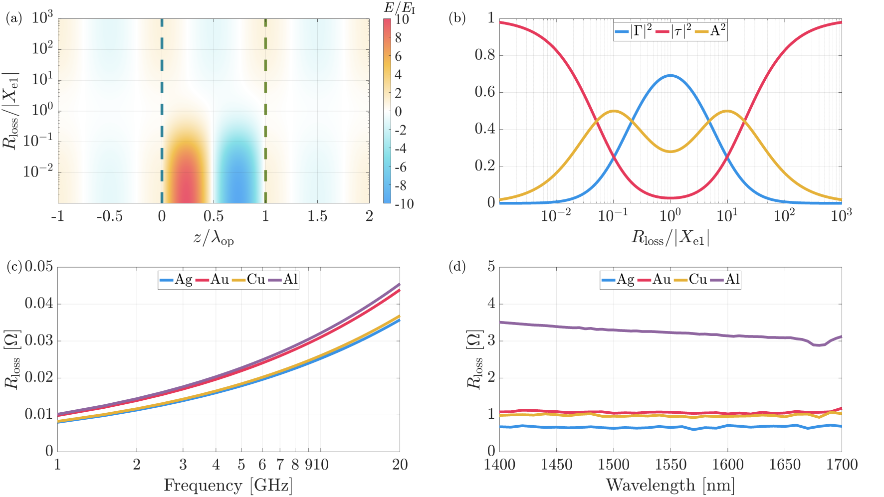
Previous analysis considered only ideal lossless metasurfaces, which is unrealistic in practice as losses affect performance of every device to some degree. Therefore, it is important to analyze how the presence of dissipation loss in metasurfaces will affect the performance of the invisible cavity. Naturally, loss can be compensated in the cavity via additional energy pumping which ensures that condition (1) holds. However, in most applications, external energy pumping is not desired due to additional complexities. Therefore, we analyze the performance degradation of cavities when the impedances of both metasurfaces have additional and equal positive real parts corresponding to grid resistances:
| (18) |
Taking into account the dissipation loss, the total electric field across the cavity is modified, as shown in Fig. 14(a). If the grid losses are much greater than the reactances (in the absolute values), both metasurfaces are weakly excited, resulting in low scattering and low field amplitude inside the cavity. When the metasurface resistance is comparable to the reactance, the cavity becomes reflective and also absorption increases, as is seen in Fig. 14(b) which depicts the reflectance , transmittance , and absorbance through the cavity. The structure remains nearly non-scattering only when the ratio of the grid reactance and resistance is sufficiently small. Therefore, it is important to determine how small ratios can be achieved with realistic materials in different frequency ranges. Here, we analyze realizations in the microwave (wavelength from 1 to 20 GHz) and infrared (wavelength from 1.4 to 1.7 m) regions. We evaluate grid resistance under assumption that each metasurface represents a continuous layer of metal (gold, silver, copper, or aluminum) with a specific thickness . Naturally, metasurface patterning will result in higher (for inductive metasurfaces) or lower (for capacitive metasurfaces) values of grid resistance compared to the estimated ones. Nevertheless, such estimation gives a straightforward way to predict the influence of dissipation loss in invisible cavities.
The metallic layer can be modelled as a dielectric slab (with complex permittivity), which transmission and reflection coefficients are obtained by solving the boundary conditions between the slab and the surrounding medium [similarly as done before for the invisible resonator in Eqs. (7)]:
| (19a) | ||||
| (19b) | ||||
where and correspond to the complex wavenumber and characteristic impedance of the metallic layer. In the case that the metallic layer does not exhibit magnetic polarization (under the condition ), the metallic layer can be replaced by a metasurface with similar transmission and reflection coefficients. The equivalent grid impedance (whose resistance models dissipation effects) is obtained from the analysis of a single metasurface:
| (20) |
In the microwave range, metals can be considered as good conductors with
| (21) |
where is the metal conductance, is the operational frequency and is the metal permeability (being equal to , vacuum’s permeability, for the selected metals) [48]. In this analysis, the assumed slab thickness is (around at 9 GHz), using metal conductivities from Ref. [48]. The analytical results in Fig. 14(c) demonstrate that in the microwave region the dissipation loss in metasurfaces is very small and can be neglected unless the ratio is not small. Using Fig. 14(b), one can estimate the minumum reactance which one can achieve without compromising the cavity operation. For example, at a frequency of 11 GHz, one can design copper invisible cavity with reactance , providing that the transmittance will be not less than 90%. Such small reactance ensures cavity Q-factor of the order of , as is seen from Fig. 3(b).
Metals cannot be considered as good conductors at near-infrared frequencies, therefore, propagation parameters are written in a more way as
| (22) |
For this analysis, we choose the slab thickness (approximately of the wavelength ). Using metal parameters from Ref. [49], it was found that dissipation in metals is high and cannot be neglected [see Fig. 14(d)]. In order to achieve high-Q invisible cavities in this range, one should use plasmonic metasurfaces with external energy pumping [32] or design invisible cavities based on high-permittivity dielectric metasurfaces (e.g., [50]). In the latter case, one can envisage realization of metasurfaces using arrays of subwavelength dielectric spheres or cylinders operating near the electric resonance. One metasurface operates at the frequency slightly below the resonance (negative ) and the other one slightly above the resonance (positive ).
Appendix D:
Reflection and transmission through the cavity with an arbitrary object placed inside
Consider the scenario of a scattering object positioned inside an invisible resonator at , as shown in Fig. 15. Without loss of generality, the object is modelled as a metasurface whose electric current density is given by the grid impedance and the average electric field at its plane.
Under these circumstances, the generalized sheet transition conditions are similar to those found in Eqs. (7), with the addition of the discontinuities produced by the object:
| (23a) | ||||
| (23b) | ||||
where the forward and backward propagating waves in front of and behind the object are denoted with subindices “1” and “2”, respectively; and is the electric current density induced in the object, defined as
| (24) |
The boundary conditions, after applying invisibility conditions compatible with Eqs. (1), lead to the following transfer functions:
| (25a) | ||||
| (25b) | ||||
| (25c) | ||||
The results of Fig. 9 were obtained by calculating transmission and reflection coefficients of Eqs. (25) for an object with variable grid impedance located at the field maximum/minimum given by Eqs. (13). As the two metasurfaces forming the invisible resonator are lossless, the power absorbed in the object can be found as
| (26) |
References
- [1] R. Soref, “The past, present, and future of silicon photonics,” IEEE Journal of Selected Topics in Quantum Electronics, vol. 12, no. 6, pp. 1678–1687, Nov 2006.
- [2] A. F. Koenderink, A. Alù, and A. Polman, “Nanophotonics: Shrinking light-based technology,” Science, vol. 348, no. 6234, pp. 516–521, Apr 2015.
- [3] C. Fabry and A. Perot, “Théorie et applications d’ une nouvelle méthodes de spectroscopie interférentielle,” Annales de Chimie, vol. 16, no. 7, pp. 115–144, 1899.
- [4] A. Perot and C. Fabry, “On the application of interference phenomena to the solution of various problems of spectroscopy and metrology,” Astrophysical Journal, vol. 9, p. 87, Feb. 1899.
- [5] W. Culshaw, “Reflectors for a microwave Fabry-Perot interferometer,” IEEE Transactions on Microwave Theory and Techniques, vol. 7, no. 2, pp. 221–228, Apr 1959.
- [6] L. Godara, “The effect of phase-shifter errors on the performance of an antenna-array beamformer,” IEEE Journal of Oceanic Engineering, vol. 10, no. 3, pp. 278–284, July 1985.
- [7] A. Dandridge and A. B. Tveten, “Phase compensation in interferometric fiber-optic sensors,” Opt. Lett., vol. 7, no. 6, pp. 279–281, Jun 1982.
- [8] K. Akiyama, A. Alberdi, W. Alef, K. Asada, R. Azulay, A.-K. Baczko, D. Ball, M. Baloković, J. Barrett, D. Bintley et al., “First M87 event horizon telescope results. II. Array and instrumentation,” The Astrophysical Journal Letters, vol. 875, no. 1, p. L2, 2019.
- [9] P. Ehrenfest, “Ungleichförmige elektrizitätsbewegungen ohne magnet-und strahlungsfeld,” Phys. Z, vol. 11, pp. 708–709, 1910.
- [10] M. Kerker, “Invisible bodies,” J. Opt. Soc. Am., vol. 65, no. 4, pp. 376–379, Apr 1975.
- [11] A. J. Devaney, “Nonuniqueness in the inverse scattering problem,” Journal of Mathematical Physics, vol. 19, no. 7, pp. 1526–1531, 1978.
- [12] G. Gbur, “Nonradiating sources and other ‘invisible’ objects,” in Progress in Optics, E. Wolf, Ed. Elsevier Science Pub Co, 2003, vol. 45, ch. 5, pp. 273–316.
- [13] A. E. Miroshnichenko, A. B. Evlyukhin, Y. F. Yu, R. M. Bakker, A. Chipouline, A. I. Kuznetsov, B. Luk’yanchuk, B. N. Chichkov, and Y. S. Kivshar, “Nonradiating anapole modes in dielectric nanoparticles,” Nature Communications, vol. 6, no. 1, Aug 2015.
- [14] A. Epstein and G. V. Eleftheriades, “Huygens’ metasurfaces via the equivalence principle: Design and applications,” Journal of the Optical Society of America B, vol. 33, no. 2, p. A31, Jan 2016.
- [15] A. A. Elsakka, V. S. Asadchy, I. A. Faniayeu, S. N. Tcvetkova, and S. A. Tretyakov, “Multifunctional cascaded metamaterials: Integrated transmitarrays,” IEEE Transactions on Antennas and Propagation, vol. 64, no. 10, pp. 4266–4276, Oct 2016.
- [16] C. W. Hsu, B. Zhen, A. D. Stone, J. D. Joannopoulos, and M. Soljačić, “Bound states in the continuum,” Nature Reviews Materials, vol. 1, no. 9, p. 16048, Jul 2016.
- [17] J. von Neuman and E. Wigner, “Über merkwürdige diskrete Eigenwerte. Über das Verhalten von Eigenwerten bei adiabatischen Prozessen,” Physikalische Zeitschrift, vol. 30, pp. 467–470, 1929.
- [18] F. H. Stillinger and D. R. Herrick, “Bound states in the continuum,” Physical Review A, vol. 11, pp. 446–454, Feb 1975.
- [19] D. C. Marinica, A. G. Borisov, and S. V. Shabanov, “Bound states in the continuum in photonics,” Physical Review Letters, vol. 100, no. 18, May 2008.
- [20] N. Moiseyev, “Suppression of Feshbach resonance widths in two-dimensional waveguides and quantum dots: A lower bound for the number of bound states in the continuum,” Physical Review Letters, vol. 102, no. 16, Apr 2009.
- [21] Y. Plotnik, O. Peleg, F. Dreisow, M. Heinrich, S. Nolte, A. Szameit, and M. Segev, “Experimental observation of optical bound states in the continuum,” Physical Review Letters, vol. 107, p. 183901, Oct 2011.
- [22] F. Monticone and A. Alú, “Embedded photonic eigenvalues in 3D nanostructures,” Physical Review Letters, vol. 112, no. 21, p. 213903, May 2014.
- [23] M. G. Silveirinha, “Trapping light in open plasmonic nanostructures,” Physical Review A, vol. 89, no. 2, p. 023813, Feb. 2014.
- [24] S. Lannebère and M. G. Silveirinha, “Optical meta-atom for localization of light with quantized energy,” Nature Communications, vol. 6, p. 8766, Oct. 2015.
- [25] I. Liberal and N. Engheta, “Nonradiating and radiating modes excited by quantum emitters in open epsilon-near-zero cavities,” Science Advances, vol. 2, no. 10, p. e1600987, Oct. 2016.
- [26] Z. F. Sadrieva, I. S. Sinev, A. K. Samusev, I. V. Iorsh, A. A. Bogdanov, R. Malureanu, and A. V. Lavrinenko, “Optical bound state in the continuum in the one-dimensional photonic crystal slab: Theory and experiment,” in 2016 Days on Diffraction (DD). IEEE, Jun 2016.
- [27] M. V. Rybin, K. L. Koshelev, Z. F. Sadrieva, K. B. Samusev, A. A. Bogdanov, M. F. Limonov, and Y. S. Kivshar, “High-Q supercavity modes in subwavelength dielectric resonators,” Physical Review Letters, vol. 119, no. 24, Dec 2017.
- [28] E. N. Bulgakov, D. N. Maksimov, P. N. Semina, and S. A. Skorobogatov, “Propagating bound states in the continuum in dielectric gratings,” Journal of the Optical Society of America B, vol. 35, no. 6, p. 1218, May 2018.
- [29] L. Carletti, K. Koshelev, C. D. Angelis, and Y. Kivshar, “Nonlinear nanophotonics and bound states in the continuum,” in Conference on Lasers and Electro-Optics. OSA, 2018.
- [30] K. Koshelev, A. Bogdanov, and Y. Kivshar, “Meta-optics and bound states in the continuum,” Science Bulletin, Dec 2018.
- [31] K. Koshelev, S. Lepeshov, M. Liu, A. Bogdanov, and Y. Kivshar, “Asymmetric metasurfaces with high-Q resonances governed by bound states in the continuum,” Physical Review Letters, vol. 121, no. 19, Nov 2018.
- [32] A. Krasnok and A. Alù, “Embedded scattering eigenstates using resonant metasurfaces,” Journal of Optics, vol. 20, no. 6, p. 064002, May 2018.
- [33] M. Liu and D.-Y. Choi, “Extreme Huygens’ metasurfaces based on quasi-bound states in the continuum,” Nano Letters, vol. 18, no. 12, pp. 8062–8069, 2018.
- [34] V. Bortolani, A. M. Marvin, F. Nizzoli, and G. Santoro, “Theory of Brillouin scattering from surface acoustic phonons in supported films,” Journal of Physics C: Solid State Physics, vol. 16, no. 9, p. 1757, 198.
- [35] C. Linton and P. McIver, “Embedded trapped modes in water waves and acoustics,” Wave Motion, vol. 45, no. 1, pp. 16 – 29, 2007, special Issue on Localization of Wave Motion.
- [36] A. Albo, D. Fekete, and G. Bahir, “Electronic bound states in the continuum above (Ga,In)(As,N)/(Al,Ga)As quantum wells,” Physical Review B, vol. 85, p. 115307, Mar 2012.
- [37] B. Zhen, C. W. Hsu, L. Lu, A. D. Stone, and M. Soljačić, “Topological nature of optical bound states in the continuum,” Physical Review Letters, vol. 113, no. 25, Dec 2014.
- [38] H. Friedrich and D. Wintgen, “Interfering resonances and bound states in the continuum,” Physical Review A, vol. 32, no. 6, pp. 3231–3242, Dec 1985.
- [39] A. Kodigala, T. Lepetit, Q. Gu, B. Bahari, Y. Fainman, and B. Kanté, “Lasing action from photonic bound states in continuum,” Nature, vol. 541, no. 7636, pp. 196–199, Jan 2017.
- [40] S. Romano, G. Zito, S. Torino, G. Calafiore, E. Penzo, G. Coppola, S. Cabrini, I. Rendina, and V. Mocella, “Label-free sensing of ultralow-weight molecules with all-dielectric metasurfaces supporting bound states in the continuum,” Photonics Research, vol. 6, no. 7, p. 726, Jun 2018.
- [41] S. T. Ha, Y. H. Fu, N. K. Emani, Z. Pan, R. M. Bakker, R. Paniagua-Domínguez, and A. I. Kuznetsov, “Directional lasing in resonant semiconductor nanoantenna arrays,” Nature Nanotechnology, vol. 13, no. 11, pp. 1042–1047, Aug 2018.
- [42] S. B. Glybovski, S. A. Tretyakov, P. A. Belov, Y. S. Kivshar, and C. R. Simovski, “Metasurfaces: From microwaves to visible,” Physics Reports, vol. 634, pp. 1–72, May 2016.
- [43] N. Yu and F. Capasso, “Flat optics with designer metasurfaces,” Nature Materials, vol. 13, no. 2, pp. 139–150, Feb 2014.
- [44] B. A. Munk, Frequency selective surfaces: Theory and design. John Wiley & Sons, 2005.
- [45] Y. Ra’di, D. L. Sounas, A. Alù, and S. A. Tretyakov, “Parity-time-symmetric teleportation,” Physical Review B, vol. 93, no. 23, Jun 2016.
- [46] X. Ma, M. S. Mirmoosa, and S. A. Tretyakov, “Parallel-plate waveguides formed by arbitrary impedance sheets,” arXiv e-prints, p. arXiv:1901.04920, Jan 2019.
- [47] H. Van de Stadt and J. M. Muller, “Multimirror Fabry–Perot interferometers,” JOSA A, vol. 2, no. 8, pp. 1363–1370, 1985.
- [48] D. M. Pozar, Microwave Engineering. J. Wiley & Sons, Inc, 2011.
- [49] K. M. McPeak, S. V. Jayanti, S. J. P. Kress, S. Meyer, S. Iotti, A. Rossinelli, and D. J. Norris, “Plasmonic films can easily be better: Rules and recipes,” ACS Photonics, vol. 2, no. 3, pp. 326–333, 2015, pMID: 25950012.
- [50] P. Genevet, F. Capasso, F. Aieta, M. Khorasaninejad, and R. Devlin, “Recent advances in planar optics: From plasmonic to dielectric metasurfaces,” Optica, vol. 4, no. 1, p. 139, Jan 2017.