Commensurability Oscillations in One-Dimensional Graphene Superlattices
Abstract
We report the experimental observation of commensurability oscillations (COs) in 1D graphene superlattices. The widely tunable periodic potential modulation in hBN encapsulated graphene is generated via the interplay of nanopatterned few layer graphene acting as a local bottom gate and a global Si back gate. The longitudinal magneto-resistance shows pronounced COs, when the sample is tuned into the unipolar transport regime. We observe up to six CO minima, providing evidence for a long mean free path despite the potential modulation. Comparison to existing theories shows that small angle scattering is dominant in hBN/graphene/hBN heterostructures. We observe robust COs persisting to temperature exceeding K. At high temperatures, we find deviations from the predicted -dependence, which we ascribe to electron-electron scattering.
Due to its high intrinsic mobility Morozov et al. (2008), graphene is an ideal material for exploring ballistic phenomena. Both suspended graphene Du et al. (2008); Bolotin et al. (2008) and graphene-hexagonal boron nitride (hBN) heterostructures Dean et al. (2010); Wang et al. (2013) were employed to demonstrate integer and fractional quantum Hall effects Young et al. (2012); Bolotin et al. (2009); Du et al. (2009); Li et al. (2017), conductance quantization Tombros et al. (2011); Terrés et al. (2016), cyclotron orbits Taychatanapat et al. (2013); Lee et al. (2016); Sandner et al. (2015); Yagi et al. (2015), and ballistic effects at p-n-junctions Rickhaus et al. (2013, 2015); Lee et al. (2015), all requiring high mobility.
In particular, several fascinating observations have been made in moiré superlattices in graphene/hBN heterostructures. In addition to magnetotransport signatures Dean et al. (2013); Hunt et al. (2013); Ponomarenko et al. (2013) of the fractal energy spectrum predicted by Hofstadter Hofstadter (1976), Krishna Kumar et al. recently reported robust periodic oscillations persisting to above room temperature Krishna Kumar et al. (2017). Those oscillations were ascribed to band conductivity in superlattice-induced minibands, where the group velocity in those minibands enters into the magnetoconductance. Here, the oscillation period is independent of the carrier density and set only by the lattice spacing via , where is the magnetic flux quantum and the flux through one superlattice unit cell.
However, the archetypal effect where a superlattice potential leads to magnetoresistance oscillations due to miniband conductivity, namely Weiss or commensurability oscillations (CO) Weiss et al. (1989), has not yet been demonstrated in graphene, owing to the challenging task of combining high mobility graphene and a weak nanometer scale periodic potential. Those oscillations arise due to the interplay between the cyclotron orbits of electrons in a high magnetic field and the superlattice potential. For a 1D modulation, pronounced -periodic oscillations in the magnetoresistance are observed, with minima appearing whenever the cyclotron diameter is a multiple of the lattice period , following the relation
| (1) |
with being an integer. This intuitive picture was confirmed in Beenakker’s semiclassical treatment Beenakker (1989). Quantum mechanically, without modulation and at high magnetic field, Landau levels are highly degenerate in the quantum number . The superlattice potential lifts the degeneracy and introduces a miniband dispersion into each Landau level. The miniband width oscillates with both and energy, and flat bands appear whenever Eq. (1) is fulfilled. Therefore, the group velocity also oscillates, leading to magnetoconductance oscillations Gerhardts et al. (1989); Winkler et al. (1989). Those oscillations persist to higher temperatures than Shubnikov de Haas oscillations (SdHO) since the band conductivity survives thermal broadening of the density of states. In contrast to the oscillations in Ref. Krishna Kumar et al. (2017), the COs depend on the electron density through , where () is the spin (valley) degeneracy. The commensurability condition Eq. (1) also holds in the case of graphene Matulis and Peeters (2007); Tahir et al. (2007). What is different, though, is the Landau level spectrum which is equidistant in the case of a conventional 2DEG but has a square root dependence in case of the Dirac fermions in graphene Novoselov et al. (2005); Zhang et al. (2005). This has been predicted to also modify the COs Matulis and Peeters (2007); Tahir et al. (2007); Nasir et al. (2010). Notably, Matulis and Peeters calculated very robust COs in the quasiclassical region of small fields that should persist up to high temperatures Matulis and Peeters (2007).
Here we employ a patterned few-layer graphene backgating scheme Li et al. (2016); Drienovsky et al. (2017) to demonstrate clear cut COs of both Dirac electrons and holes in high-mobility graphene, subjected to a weak unidirectional periodic potential. Contrary to hBN/graphene moiré lattices, where lattice parameters are set by the materials properties of graphene and hBN, this enables us to define an arbitrary superlattice geometry and strength. As the usual technique of placing a metallic grating with nanoscale periodicity fails due to the poor adhesion of metal to the atomically smooth and inert hBN surface we resort to including a patterned bottom gate (PBG) consisting of few layer graphene (FLG) carrying the desired superlattice pattern into the usual van der Waals stacking and edge-contacting technique Wang et al. (2013). The hBN/graphene/hBN stack is assembled on top of the PBG. Importantly, the bottom hBN layer has to be kept very thin () to impose the periodic potential effectively onto the unpatterned graphene sheet. For the PBG, we exfoliated a FLG sheet (3-4 layers) onto an oxidized, highly p-doped silicon wafer which served as a uniform global back gate in the measurements. The FLG sheet was patterned into the desired shape by electron beam lithography and oxygen plasma etching. This approach exploits the atomic flatness of FLG, which makes it a perfect gate electrode for 2D-material heterostructures that can be easily etched into various shapes, e.g. 1D or 2D superlattices, split gates, collimators Cheianov and Fal’ko (2006) or lenses Liu et al. (2017), and allows for nanoscale manipulation of the carrier density. Figure 1a shows the AFM image of an -stripe lattice used for fabrication of sample B, discussed below. The hBN/graphene/hBN stack was deposited onto the PBG, and a mesa was defined by reactive ion etching (Fig. 1b). We used a sequential etching method, employing SF6 Pizzocchero et al. (2016), O2 and CHF3/O2-processes, in order to avoid damage to the thin hBN bottom layer covering the PBG (see Supplemental Material for details Note (2)). Edge contacts of evaporated Cr/Au (1 nm/ 90 nm) were deposited after reactive ion etching of the contact region and a brief exposure to oxygen plasma. More details on the fabrication are reported elsewhere Drienovsky et al. (2017).
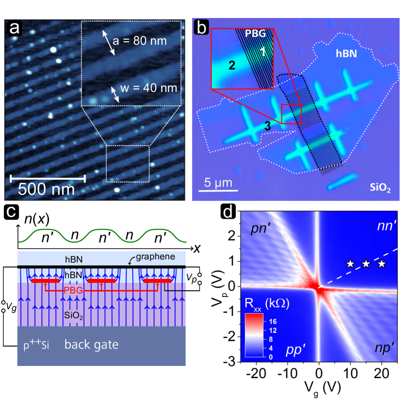
The combined action of PBG and the global gate is sketched in Fig. 1c. The PBG partially screens the electric field lines emerging from the Si back gate. The latter therefore controls the carrier type and density in the regions between stripes (labeled ), whereas the PBG itself controls primarily those directly above the stripes (labeled ). A typical charge carrier density profile for a weak potential modulation in the unipolar transport regime is shown atop. Hence, tuning both gates separately we can generate unipolar or bipolar potential modulation on the nanoscale.
Transport measurements were performed in a helium cryostat at temperatures between and and in perpendicular magnetic fields between to using low frequency lock-in techniques at a bias current of 10 nA. We present data from two samples (A and B) with a 1D-superlattice period of and , respectively. The PBGs of both samples, A and B, consist of 19 and 40 stripes of few layer graphene (thickness 3 to 4 layers), respectively. The thicknesses of the lower hBN, separating the graphene from the PBG are and , respectively, measured with AFM. Fig. 1d displays the zero field resistance of sample A. Using both gates, we can tune into the unipolar regime of comparatively low resistance (labeled and ) as well as into the bipolar regime (labeled and ), where pronounced Fabry-Pérot oscillations appear Young and Kim (2009); Rickhaus et al. (2013); Drienovsky et al. (2014); Handschin et al. (2017); Drienovsky et al. (2017); Dubey et al. (2013). Their regular shape proves the high quality and uniformity of the superlattice potential. The electrostatics of dual gated samples and different transport regimes were discussed, e.g., in Refs. Rickhaus et al. (2013); Drienovsky et al. (2014, 2017); Dubey et al. (2013).
Below, we focus on the unipolar regime, to obtain a weak and tunable 1D superlattice. This is the regime of the COs outlined above. Let us first discuss magnetotransport in sample A with mobility (see Supplemental Material Note (2) for the determination of mobility in both samples). In Fig. 2a-c we show three magnetic field sweeps, where we keep the PBG-voltage fixed at and tune the modulation strength by varying the backgate voltage . The sweeps represent three different situations, (a) , (b) and (c) . The corresponding -positions of the sweeps a-c are marked by stars in the -quadrant of Fig. 1d. Moreover, the inset in Fig. 2b shows the corresponding charge carrier density profiles that were calculated employing a 1D electrostatic model of the device, including a quantum capacitance correction Drienovsky et al. (2014); Liu (2013), but neglecting screening.
In Fig. 2a a weak, unipolar () potential modulation is shown where the longitudinal resistance exhibits well pronounced peaks and dips prior to the emergence of SdHOs, appearing at slightly higher -fields. The average charge carrier density, extracted from SdHOs is for this particular gate configuration, yielding a mean free path . The expected flat band positions (Eq. (1)), are denoted by the blue vertical dotted lines, perfectly describing the experimentally observed minima. The dips are resolved up to , corresponding to a cyclotron orbit circumference of . This clearly confirms that ballistic transport is maintained over several periods of the superlattice.
At (Fig. 2b), holds (see inset in Fig. 2b). We still observe clear SdHOs, but the COs disappeared. The pronounced peak at can be attributed to a magneto-size effect related to boundary scattering in ballistic conductors Thornton et al. (1989); Beenakker and van Houten (1991) of width . While in GaAs based 2DEGs, a ratio is found, we extract in accordance with previous studies on graphene Masubuchi et al. (2012).
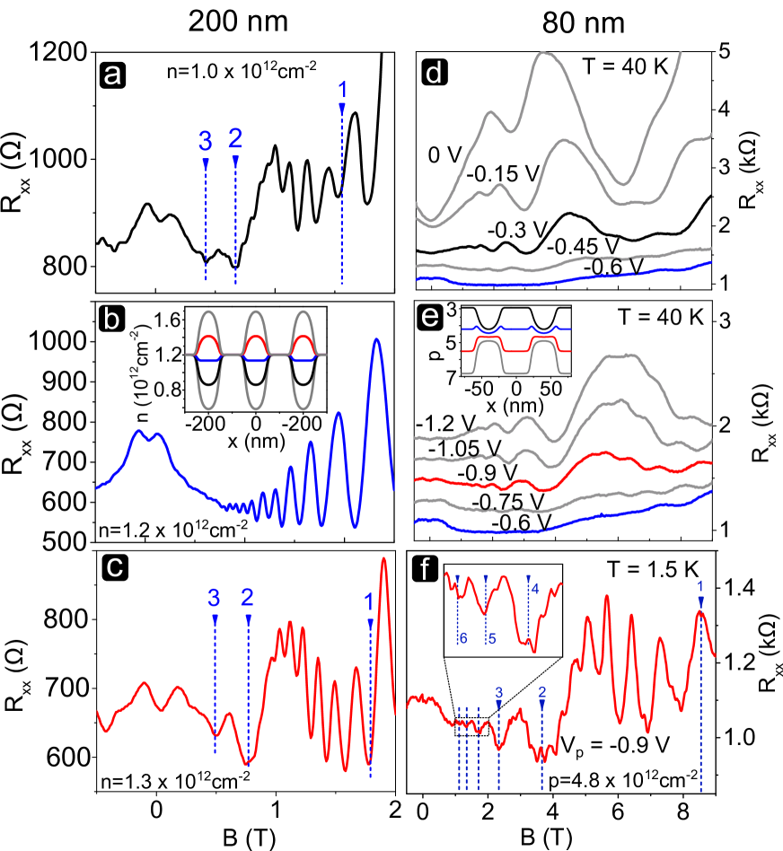
Further increasing increases and switches the modulation on again (). The SdHOs in Fig. 2c yield an average . Again, three minima appear at the expected flat band condition described by Eq. (1).
Let us turn to sample B, where we demonstrate COs in the p regime. It has a short period of and a bottom hBN flake of only thickness, separating the PBG from the graphene. Figure 2d,e shows the longitudinal resistance at high average hole densities () as a function of the PBG-voltage and the perpendicular B-field at fixed (Dirac-point at ) and . Here, was increased in order to damp the SdHOs for better resolution of the COs. The mobility of and the rather large hole density give rise to a mean free path . We can resolve COs up to (see Fig. 2f 111Fine features in Fig. 2f are presumably due to mesoscopic fluctuations.), corresponding to a cyclotron orbit circumference of , which is about twice in the average density range considered. At around the COs disappear as the modulation potential becomes minimal (blue lines in Figs. 2d,e, cf. charge carrier density profile in the inset) Here, holds and no COs are resolvable. This changes again at (Fig. 2e). As the back gate voltage is further increased, strong COs appear again, with the minima positions shifting according to the density dependence of Eq. (1) (see also Supplemental Material for a color map Note (2)). The observation of clear cut COs in density modulated hole and electron systems for distinctively different superlattice periods highlights the suitability of graphene PBGs for imposing lateral potentials on graphene films.
As pointed out in the introduction, theory predicted enhanced COs in graphene Matulis and Peeters (2007). To check this and to compare theory and experiment we apply the different prevailing theoretical models to describe for our sample. The amplitude of the COs is governed by the period , the modulation amplitude and the Drude transport relaxation time . Expressions for the additional band conductivity for 2DEG in Peeters and Vasilopoulos (1992) and graphene in Matulis and Peeters (2007) (Eqs. S1, S9 in Supplemental Material, respectively Note (2)), are linear in and tend to overestimate the CO amplitude at lower field. Mirlin and Wölfle Mirlin and Wölfle (1998) introduced anisotropic scattering to the problem by taking into account the small angle impurity scattering, allowing for a high ratio of the momentum relaxation time to the elastic scattering time (Eq. S10, Supplemental Material Note (2)). In this approach, both the damping of COs at lower fields and the modulation amplitudes of conventional 2DEGs are correctly described. For the graphene case, Matulis and Peeters employed the Dirac-type Landau level spectrum, as opposed to the parabolic 2DEG situation Matulis and Peeters (2007), leading to a modified expression. In their approach, only a single transport scattering time was included. The temperature dependence of the COs was treated in Refs. Beton et al. (1990); Peeters and Vasilopoulos (1992) for parabolic 2DEGs and in Ref. Matulis and Peeters (2007) for graphene. It is expected to exhibit a -dependence, where with the critical temperature
| (2) |
Here, is the Boltzmann constant and the difference between parabolic and linear dispersion is absorbed in the different Fermi velocities .
To compare to the different theoretical models, we extracted the elastic scattering time from the SdHO-envelope Monteverde et al. (2010) of a reference Hall bar (see Supplemental Material for details Note (2)). With , we obtain the ratio , which emphasizes the importance of small angle scattering in hBN-encapsulated graphene. The experimental (black) curve in Fig. 3a was taken at , where the SdHOs are already visibly suppressed, but the amplitude of the COs is practically unchanged, allowing for a better comparison to theory. We first compare our measurement to the graphene theory employing isotropic scattering only. Since the superlattice period , , temperature and the average charge carrier density are known, only the relative modulation strength remains as a fitting parameter. By fitting the theoretical expressions (for details see Supplemental Material Note (2)) to the CO peak at T in Fig. 3a we obtain . At lower fields, the experimentally observed oscillations decay much faster than the calculated ones. Inserting our sample parameters into the theory employing small angle impurity scattering Mirlin and Wölfle (1998) (Eq. S10, Supplemental Material Note (2)), again only remains as a free fitting parameter, and we obtain the red trace using . The fit describes the experimental magnetoresistance strikingly well, although the Dirac nature of the spectrum was not considered. The fits in Fig. 3a imply that including small angle impurity scattering is essential for the correct description of encapsulated graphene.
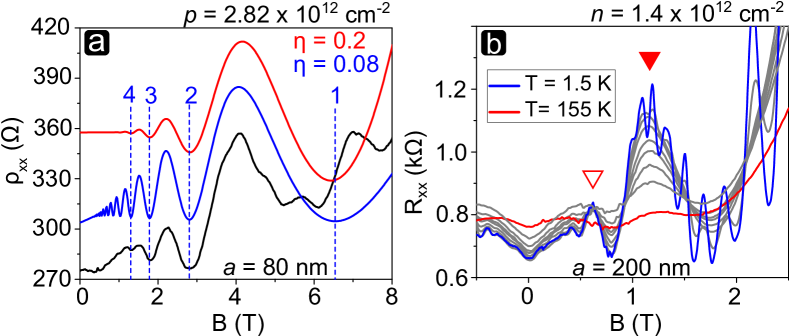
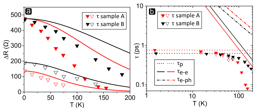
Finally, we discuss the temperature dependence of COs in 1D modulated graphene. Figure 3b depicts a longitudinal resistance trace of sample A at at different temperatures. The graph clearly demonstrates that the COs are much more robust than the SdHOs. While the latter are almost completely suppressed at , the COs survive at least up to (Sample A) and (Sample B), respectively. We analyze the temperature evolution of the first two CO-peaks (marked by red triangles), using the connecting line between two adjacent minima as the bottom line to evaluate the height of the maximum in between. We adopt this procedure described by Beton et al. for a better comparison to experiments in GaAs Beton et al. (1990). The temperature dependence of the two peaks is shown in Fig. 4a. Also shown are the corresponding data of sample B (black symbols). The data for sample B were extracted at much higher fields, due to the smaller lattice period and higher carrier density, leading to a weaker temperature dependence in Eq. (2). The expected temperature dependence (solid lines) Beton et al. (1990); Peeters and Vasilopoulos (1992); Matulis and Peeters (2007), clearly deviates from the experimental data points. For GaAs, -dependent damping of the COs was so strong that the assumption of a -independent scattering time was justified Beton et al. (1990). In graphene, the higher leads to a higher and therefore the COs persist to higher temperatures than in GaAs. Hence, we have to consider a -dependence of the scattering time as well. Using the low-temperature momentum relaxation time we first determine the modulation strength , Then, using a fixed , we extract the scattering time entering into the CO theory at elevated temperatures. The extracted times are plotted in Fig. 4b for both samples and two magnetic fields each, together with predictions for the electron-electron scattering time Kumar et al. (2017) and electron-phonon scattering time Hwang and Das Sarma (2008). Clearly, at K, deviates visibly from , with being the relevant cut-off, while is not important. This resembles the recently found observation window for hydrodynamic effects in graphene Ho et al. (2018).
To conclude, we present the first experimental evidence of commensurability oscillations (COs) Weiss et al. (1989) for both electrons and holes in a hBN-encapsulated monolayer graphene subject to a 1D periodic potential. This was made possible through the combined action of a nanopatterned FLG bottom gate and a global Si back gate. Our approach allows tuning both carrier density and modulation strength independently in a wide range, and on the scale of a few tens of nanometers. The minima in are well described by the flat band condition (1). The predicted strong temperature robustness of COs in graphene was qualitatively confirmed, but detailed comparison to existing theories emphasized the need for a description including anisotropic scattering of charge carriers in encapsulated graphene. Using data at elevated temperature, we could extract the -dependence of the scattering time, pointing to electron-electron scattering as the high- cutoff for the CO amplitude.
Acknowledgements.
Financial support by the Deutsche Forschungsgemeinschaft (DFG) within the programs GRK 1570 and SFB 689 (projects A7 and A8) and project Ri 681/13 “Ballistic Graphene Devices” and by the Taiwan Minister of Science and Technology (MOST) under Grant No. 107-2112-M-006-004-MY3 is gratefully acknowledged. Growth of hexagonal boron nitride crystals was supported by the Elemental Strategy Initiative conducted by the MEXT, Japan and JSPS KAKENHI Grant Numbers JP15K21722. We thank J. Amann, C. Baumgartner, A. T. Nguyen and J. Sahliger for their contribution towards the optimization of the fabrication procedure.References
- Morozov et al. (2008) S. V. Morozov, K. S. Novoselov, M. I. Katsnelson, F. Schedin, D. C. Elias, J. A. Jaszczak, and A. K. Geim, Phys. Rev. Lett. 100, 016602 (2008).
- Du et al. (2008) X. Du, I. Skachko, A. Barker, and E. Y. Andrei, Nature Nanotechnology 3, 491 (2008).
- Bolotin et al. (2008) K. Bolotin, K. Sikes, Z. Jiang, M. Klima, G. Fudenberg, J. Hone, P. Kim, and H. Stormer, Solid State Communications 146, 351 (2008).
- Dean et al. (2010) C. R. Dean, A. F. Young, I. Meric, C. Lee, L. Wang, S. Sorgenfrei, K. Watanabe, T. Taniguchi, P. Kim, K. L. Shepard, and J. Hone, Nat. Nanotech. 5, 722 (2010).
- Wang et al. (2013) L. Wang, I. Meric, P. Huang, Q. Gao, Y. Gao, H. Tran, T. Taniguchi, K. Watanabe, L. Campos, D. Muller, et al., Science 342, 614 (2013).
- Young et al. (2012) A. F. Young, C. R. Dean, L. Wang, H. Ren, P. Cadden-Zimansky, K. Watanabe, T. Taniguchi, J. Hone, K. L. Shepard, and P. Kim, Nature Physics 8, 550 (2012).
- Bolotin et al. (2009) K. I. Bolotin, F. Ghahari, M. D. Shulman, H. L. Stormer, and P. Kim, Nature 462, 196 (2009).
- Du et al. (2009) X. Du, I. Skachko, F. Duerr, A. Luican, and E. Y. Andrei, Nature 462, 192 (2009).
- Li et al. (2017) J. I. A. Li, C. Tan, S. Chen, Y. Zeng, T. Taniguchi, K. Watanabe, J. Hone, and C. R. Dean, Science 358, 648 (2017)..
- Tombros et al. (2011) N. Tombros, A. Veligura, J. Junesch, M. H. D. Guimaraes, I. J. Vera-Marun, H. T. Jonkman, and B. J. van Wees, Nat Phys 7, 697 (2011).
- Terrés et al. (2016) B. Terrés, L. A. Chizhova, F. Libisch, J. Peiro, D. Jörger, S. Engels, A. Girschik, K. Watanabe, T. Taniguchi, S. V. Rotkin, J. Burgdörfer, and C. Stampfer, Nature Communications 7, 11528 (2016).
- Taychatanapat et al. (2013) T. Taychatanapat, K. Watanabe, T. Taniguchi, and P. Jarillo-Herrero, Nature Physics 9, 225 (2013).
- Lee et al. (2016) M. Lee, J. R. Wallbank, P. Gallagher, K. Watanabe, T. Taniguchi, V. I. Fal’ko, and D. Goldhaber-Gordon, Science 353, 1526 (2016)..
- Sandner et al. (2015) A. Sandner, T. Preis, C. Schell, P. Giudici, K. Watanabe, T. Taniguchi, D. Weiss, and J. Eroms, Nano Letters 15, 8402 (2015).
- Yagi et al. (2015) R. Yagi, R. Sakakibara, R. Ebisuoka, J. Onishi, K. Watanabe, T. Taniguchi, and Y. Iye, Physical Review B 92, 195406 (2015).
- Rickhaus et al. (2013) P. Rickhaus, R. Maurand, M.-H. Liu, M. Weiss, K. Richter, and C. Schönenberger, Nat. Commun. 4, 2342 (2013).
- Rickhaus et al. (2015) P. Rickhaus, M.-H. Liu, P. Makk, R. Maurand, S. Hess, S. Zihlmann, M. Weiss, K. Richter, and C. Schönenberger, Nano Letters 15, 5819 (2015).
- Lee et al. (2015) G.-H. Lee, G.-H. Park, and H.-J. Lee, Nature Physics 11, 925 (2015).
- Dean et al. (2013) C. R. Dean, L. Wang, P. Maher, C. Forsythe, F. Ghahari, Y. Gao, J. Katoch, M. Ishigami, P. Moon, M. Koshino, T. Taniguchi, K. Watanabe, K. L. Shepard, J. Hone, and P. Kim, Nature 497, 598 (2013).
- Hunt et al. (2013) B. Hunt, J. Sanchez-Yamagishi, A. Young, M. Yankowitz, B. J. LeRoy, K. Watanabe, T. Taniguchi, P. Moon, M. Koshino, P. Jarillo-Herrero, et al., Science 340, 1427 (2013).
- Ponomarenko et al. (2013) L. A. Ponomarenko, R. V. Gorbachev, G. L. Yu, D. C. Elias, R. Jalil, A. A. Patel, A. Mishchenko, A. S. Mayorov, C. R. Woods, J. R. Wallbank, M. Mucha-Kruczynski, B. A. Piot, P. M, I. V. Grigoreva, K. S. Novoselov, F. Guinea, V. I. Fal’ko, and A. K. Geim, Nature 497, 594 (2013).
- Hofstadter (1976) D. R. Hofstadter, Physical Review B 14, 2239 (1976).
- Krishna Kumar et al. (2017) R. Krishna Kumar, X. Chen, G. H. Auton, A. Mishchenko, D. A. Bandurin, S. V. Morozov, Y. Cao, E. Khestanova, M. Ben Shalom, A. V. Kretinin, K. S. Novoselov, L. Eaves, I. V. Grigorieva, L. A. Ponomarenko, V. I. Fal’ko, and A. K. Geim, Science 357, 181 (2017)..
- Weiss et al. (1989) D. Weiss, K. Klitzing, K. Ploog, and G. Weimann, EPL (Europhysics Letters) 8, 179 (1989).
- Beenakker (1989) C. W. J. Beenakker, Physical Review Letters 62, 2020 (1989).
- Gerhardts et al. (1989) R. Gerhardts, D. Weiss, and K. v. Klitzing, Physical Review Letters 62, 1173 (1989).
- Winkler et al. (1989) R. W. Winkler, J. P. Kotthaus, and K. Ploog, Physical Review Letters 62, 1177 (1989).
- Matulis and Peeters (2007) A. Matulis and F. M. Peeters, Physical Review B 75, 125429 (2007).
- Tahir et al. (2007) M. Tahir, K. Sabeeh, and A. MacKinnon, Journal of Physics: Condensed Matter 19, 406226 (2007).
- Novoselov et al. (2005) K. S. Novoselov, A. K. Geim, S. V. Morozov, D. Jiang, M. I. Katsnelson, I. V. Grigorieva, S. V. Dubonos, and A. A. Firsov, Nature 438, 197 (2005).
- Zhang et al. (2005) Y. Zhang, Y.-W. Tan, H. Störmer, and P. Kim, Nature 438, 201 (2005).
- Nasir et al. (2010) R. Nasir, K. Sabeeh, and M. Tahir, Physical Review B 81, 085402 (2010).
- Li et al. (2016) J. Li, K. Wang, K. J. McFaul, Z. Zern, Y. Ren, K. Watanabe, T. Taniguchi, Z. Qiao, and J. Zhu, Nature Nanotechnology 11, 1060 (2016).
- Drienovsky et al. (2017) M. Drienovsky, A. Sandner, C. Baumgartner, M.-H. Liu, T. Taniguchi, K. Watanabe, K. Richter, D. Weiss, and J. Eroms, arXiv preprint arXiv:1703.05631 (2017).
- Cheianov and Fal’ko (2006) V. V. Cheianov and V. I. Fal’ko, Phys. Rev. B 74, 041403 (2006).
- Liu et al. (2017) M.-H. Liu, C. Gorini, and K. Richter, Physical Review Letters 118, 066801 (2017).
- Pizzocchero et al. (2016) F. Pizzocchero, L. Gammelgaard, B. S. Jessen, J. M. Caridad, L. Wang, J. Hone, P. Bøggild, and T. J. Booth, Nature Communications 7 (2016).
- Note (2) See Supplemental Material for details of the etching procedure, additional experimental data, details on theories in GaAs and graphene, determination of scattering times, and details on the fitting to experimental data.
- Young and Kim (2009) A. F. Young and P. Kim, Nat. Phys. 5, 222 (2009).
- Drienovsky et al. (2014) M. Drienovsky, F.-X. Schrettenbrunner, A. Sandner, D. Weiss, J. Eroms, M.-H. Liu, F. Tkatschenko, and K. Richter, Phys. Rev. B 89, 115421 (2014).
- Handschin et al. (2017) C. Handschin, P. Makk, P. Rickhaus, M.-H. Liu, K. Watanabe, T. Taniguchi, K. Richter, and C. Schönenberger, Nano Lett. 17 (1), 328 (2017).
- Dubey et al. (2013) S. Dubey, V. Singh, A. K. Bhat, P. Parikh, S. Grover, R. Sensarma, V. Tripathi, K. Sengupta, and M. M. Deshmukh, Nano Lett. 13, 3990 (2013).
- Liu (2013) M.-H. Liu, Phys. Rev. B 87, 125427 (2013).
- Thornton et al. (1989) T. J. Thornton, M. L. Roukes, A. Scherer, and B. P. Van de Gaag, Physical Review Letters 63, 2128 (1989).
- Beenakker and van Houten (1991) C. Beenakker and H. van Houten, Solid State Physics 44, 1 (1991).
- Masubuchi et al. (2012) S. Masubuchi, K. Iguchi, T. Yamaguchi, M. Onuki, M. Arai, K. Watanabe, T. Taniguchi, and T. Machida, Physical Review Letters 109, 036601 (2012).
- Note (1) Fine features in Fig. 2f are presumably due to mesoscopic fluctuations.
- Peeters and Vasilopoulos (1992) F. M. Peeters and P. Vasilopoulos, Physical Review B 46, 4667 (1992).
- Mirlin and Wölfle (1998) A. D. Mirlin and P. Wölfle, Physical Review B 58, 12986 (1998).
- Beton et al. (1990) P. H. Beton, P. C. Main, M. Davison, M. Dellow, R. P. Taylor, E. S. Alves, L. Eaves, S. P. Beaumont, and C. D. W. Wilkinson, Physical Review B 42, 9689 (1990).
- Monteverde et al. (2010) M. Monteverde, C. Ojeda-Aristizabal, R. Weil, K. Bennaceur, M. Ferrier, S. Guéron, C. Glattli, H. Bouchiat, J. N. Fuchs, and D. L. Maslov, Physical Review Letters 104, 126801 (2010).
- Kumar et al. (2017) R. K. Kumar, D. A. Bandurin, F. M. D. Pellegrino, Y. Cao, A. Principi, H. Guo, G. H. Auton, M. B. Shalom, L. A. Ponomarenko, G. Falkovich, K. Watanabe, T. Taniguchi, I. V. Grigoreva, L. S. Levitov, M. Polini, and A. K. Geim, Nature Physics 13, 1182 (2017).
- Hwang and Das Sarma (2008) E. H. Hwang and S. Das Sarma, Phys. Rev. B 77, 115449 (2008).
- Ho et al. (2018) D. Y. H. Ho, I. Yudhistira, N. Chakraborty, and S. Adam, Phys. Rev. B 97, 121404 (2018).