note-name = , use-sort-key = false
Enhancement of electric and magnetic dipole transition of rare-earth doped thin films tailored by high-index dielectric nanostructures
Abstract
We propose a simple experimental technique to separately map the emission from electric and magnetic dipole transitions close to single dielectric nanostructures, using a few nanometer thin film of rare-earth ion doped clusters. Rare-earth ions provide electric and magnetic dipole transitions of similar magnitude. By recording the photoluminescence from the deposited layer excited by a focused laser beam, we are able to simultaneously map the electric and magnetic emission enhancement on individual nanostructures. In spite of being a diffraction-limited far-field method with a spatial resolution of a few hundred nanometers, our approach appeals by its simplicity and high signal-to-noise ratio. We demonstrate our technique at the example of single silicon nanorods and dimers, in which we find a significant separation of electric and magnetic near-field contributions. Our method paves the way towards the efficient and rapid characterization of the electric and magnetic optical response of complex photonic nanostructures.
In the last decades, photonic nanostructures emerged as powerful instruments to control light at the subwavelength scale.Novotny and Hecht (2006) The interest in nano-optics lies usually in the control of the optical electric field, since the response of materials to rapidly oscillating magnetic fields is extremely weak. Actually, materials with a substantial magnetic response to electromagnetic radiation (i.e. ) are not known in nature. However, properly designed nanostructures allow to significantly boost the magnetic response. For instance metallic (split-)ring resonators support a magnetic moment which is proportional to the area covered by the ring’s aperture. For frequencies in the visible range this area is usually about times larger than the equivalent area in atoms, defined by the Bohr radius, which explains the emergence of observable effects related to the optical magnetic field.Giessen and Vogelgesang (2009) In consequence, it is possible to overcome the natural limitation to by designing so-called meta-materials, which are ordered arrangements of meta-units like split-ring resonators.Pendry (2000)
Using metals requires nanostructures of complex shape to obtain a significant magnetic response. On the other hand, in dielectrics of high refractive index, a magnetic response arises naturally from the curl of the electric field.Merlin (2009); Kuznetsov et al. (2012) Very simple geometries like spheresEvlyukhin et al. (2012) or cylindersKapitanova et al. (2017) are actually sufficient to induce a strong magnetic field enhancement.Kuznetsov et al. (2016) An additional advantage of high-index dielectric nanostructures is their low dissipation. Silicon (Si) for example has a very low absorption through the entire visible range compared to noble metals.Albella et al. (2014) This weak absorption associated to the indirect gap in the near infrared becomes cumbersome only for applications involving propagation of visible light across distances of tens to hundreds of microns. Thus, in sub-micron dielectric nano-structures the absorption can usually be neglected.Albella et al. (2013) In summary, high-index nanostructures seem to provide an appropriate platform to study the confinement of optical electric and magnetic fields. Such nanostructures are indeed able to strongly localize those fields in different regions around them, while they are indistinguishable in the far field. In other words, the electric and magnetic parts of the photonic local density of states (LDOS) can be spatially separated around subwavelength small particles.Rolly et al. (2012); Wiecha et al. (2018)
The separation of magnetic and electric field energy close to photonic nano-structures was first demonstrated by measuring the local magnetic field intensity using scanning near-field optical microscopy (SNOM). The sensitivity to the magnetic part of the optical near-field is provided by particular SNOM-tips, coated with nano-scale metal rings or split-ring resonators.Devaux et al. (2000a, b); Burresi et al. (2009); Kabakova et al. (2016) Another possibility to access the electric and magnetic near-field is to use optical transitions of quantum emitters and exploit the proportionality between their decay rate and the LDOS.Girard et al. (2004); Aigouy et al. (2014); Carminati et al. (2015); Cuche et al. (2017) However, to simultaneously obtain information on the electric and magnetic near-field components, probes supporting both electric (ED) and magnetic dipole (MD) transitions need to be used. This drastically limits the range of possible emitters: ED transitions are usually 4 – 5 orders of magnitude stronger than MD transitions.Taminiau et al. (2012) Lanthanoid ions (also known as rare earth elements) such as europium (Eu3+) exhibit ED and MD transitions of similar strengthCarnall et al. (1968) and can be used as probes of the optical magnetic near field.Noginova et al. (2008); Sanz-Paz et al. (2018) A peculiarity of Eu3+ is that electric and magnetic dipole transitions of comparable strength occur at close wavelengths. ED and MD transitions of Eu3+ both start from the energy level via de-excitation to the (ED) and the level (MD).Baranov et al. (2017) Those transitions lie in the visible, around nm and nm.Noginova et al. (2008) They lie at close wavelengths but are spectrally separated enough to be easily distinguished by using color filters.
Thanks to their unique properties, rare-earth ion doped media have been used as probes to determine the relative intensities of electric and magnetic LDOS at fixed positions or on non-structured samples like interfaces.Karaveli and Zia (2011); Hussain et al. (2014); Choi et al. (2016) By attaching an Eu3+ doped nano-crystal to a SNOM tip, the D spatial distribution of the electric and magnetic LDOS on top of gold strips has been recorded.Aigouy et al. (2014) The methods employed in these studies are either based on rare-earth emitters at fixed position,Noginova et al. (2008); Choi et al. (2016) or require complex experimental setups (SNOM-type approach).Aigouy et al. (2014); Cuche et al. (2009)
In this article, we propose an alternative and complementary approach: we deposit a homogeneous nm thin film of Eu3+-doped nano-clusters on high-index dielectric nanostructures and raster-scan the sample under a tightly focused diffraction limited laser beam. In this configuration, the photoluminescence maps probe the spatial variations of the ED and MD emissions around the silicon nanostructures. We compare the results with computed maps of the electric and magnetic radiative LDOS. The results show that our far field set-up allows a fast scanning with a good signal-to-noise ratio and a good spatial resolution. Interestingly, the far field PL shows a striking similarity with the radiative LDOS.
I Photoluminescence from Eu3+-doped nanocluster film deposited on silicon nanostructures
Sample preparation
Our sample contains single crystalline silicon dimers consisting of two elements, each nm3 () large, separated by a gap of variable size. These nanostructures are fabricated in a top-down approach, where a single layer of negative-tone resist, namely hydrogen silsesquioxane (HSQ), is patterned by electron-beam lithography.Guerfi et al. (2013) Subsequent reactive ion etching in the nm Si overlayer of silicon on insulator (SOI) substrates defines the structures. The remaining HSQ-layer on the top of the structures induces an additional SiO2 capping of approximately 20nm. This layer acts as a spacer between the nanostructures and the Eu3+ doped film. For more details on the fabrication process, see Ref. Wiecha et al., 2017. After the lithography, a nm thick film of Eu3+-doped Gd2O3 nano-clusters is deposited. This thickness is a good trade-off between luminescence intensity from the emitters and planar homogeneity (see also Appendix IV.3). The film is synthesized by the Low Energy Cluster Beam Deposition (LECBD) technique. LECBD consists in the ablation of a solid Gd2O3 pellet, doped at 7% with europium, via a pulsed Nd:YAG laser ( ns pulse width). The chosen doping concentration results in a good compromise to preserve the stoichiometry of the sesquioxyde matrix as well as a high luminescence of the Europium ions, without impairing the crystallographic and optical properties of the clusters.Masenelli et al. (2012) The ablated fragments are then broken into small clusters, first by the injection of He ( mbar) as a buffer gas in the nucleation chamber and subsequently during its adiabatic expansion through a micrometer nozzle. The resulting nanocrystals are deposited on the dielectric nanostructures without further breaking (“soft landing”). More details about the process and the resulting nanocrystals can be found in Refs. Cuche et al., 2009; Perez et al., 2010.
Experimental configuration
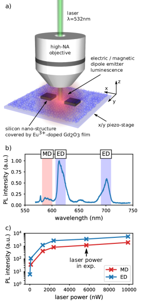
Our experimental setup consists of an optical microscope equipped for spectroscopy with a confocal pinhole of 100 µm. A simplified sketch of the experiment is shown in figure 1a. A linearly polarized cw laser at nm is focused by a air objective () on the sample, which lies on a piezo stage. The photoluminescence (PL) from the sample is collected by the same microscope objective. The PL is dispersed by a grating ( grooves per mm) and detected by a CCD camera (Andor iDus 401), with an integration time of s. A typical spectrum and saturation curve from the Eu3+-doped Gd2O3 film is shown in figure 1b-c. Finally, we obtain 2D PL maps by raster-scanning the sample under the laser with the piezo-stage. At each position, we acquire a spectrum and extract the emission intensities from the spectral ranges corresponding to magnetic or electric transitions (nm, respectively nm) during post-processing. The signal is normalized to the background PL intensity, recorded far from the nanostructures. We note that our approach yields a high signal-to-noise ratio, which can be qualitatively seen for example in the spectra (see Fig. 1b, and experimental maps in Figs. 2 and 3).
Experimental results
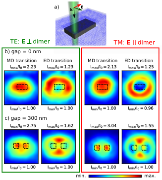
Figure 2 shows raster-scan maps, measured on silicon nanorod dimers with gap-sizes of nm and nm, obtained with an incident laser polarization perpendicular to (TE) and along (TM) the dimer long axis. In the experimental maps, a clear inversion of the contrast between emission from MD and ED transitions is observed for both polarizations. The MD PL yields a maximum intensity when the laser beam is focused on the Si blocks of the structure. On the other hand, the ED emission maps contain valley-like features with a reduced PL on top the Si blocks and an increased PL around these blocks.
Interestingly, both TE and TM configurations yield almost identical PL maps. This could be surprising at first sight as the spatial near field distribution around the Si nanodimers depends significantly on the laser polarization (see Appendix IV.1) and at our laser wavelength, ED and MD transitions in Eu3+ are both populated by excitation of the 5D1 level via the local electric field.Baranov et al. (2017); kasperczyk_excitation_2015 Furthermore, it appears that the emitters are excited close to saturation, since in Fig. 1c a plateau in the PL intensity occurs. Both considerations about the laser polarization intensity and the excitation at saturation lead to the conclusion that the observed variations in the ED (resp. MD) PL maps are predominantly driven by the electric (resp. magnetic) radiative LDOS at the emission wavelength. This conclusion is in agreement with a recent study of the directional emission of Eu3+ ions, coupled to plasmonic nanostructures. In the latter, the most significant modification of the Eu3+-PL is ascribed to the improved light out-coupling, whereas the plasmonic enhancement of the excitation has only a weak impact on the emission.Murai et al. (2017)
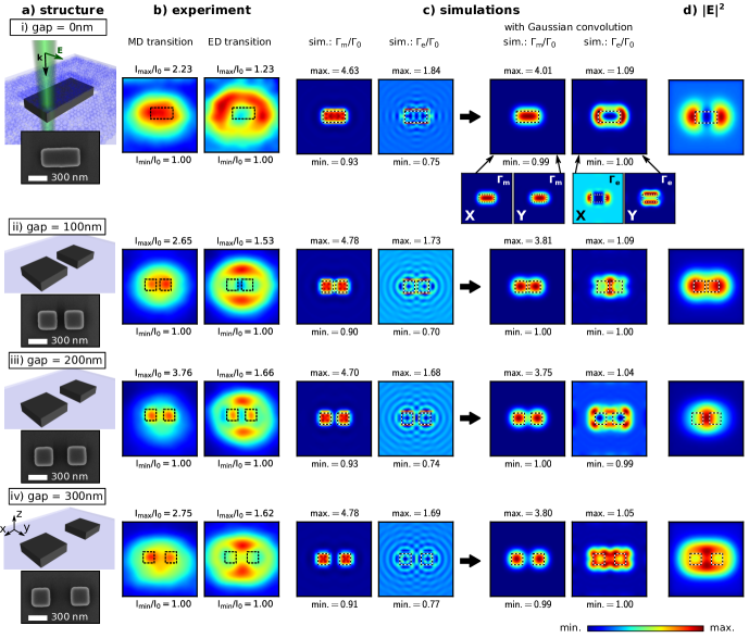
We systematically measured PL maps on silicon dimers with gap-sizes between nm and nm, which are shown in figure 3b. For these results, the laser polarization was perpendicular to the long axis of the dimers. Sketches and scanning electron microscopy (SEM) images of the corresponding structures are shown in Fig. 3a. As already observed in figure 2, a clear inversion of the contrast between emission from MD and ED transitions is observed. A single nano-rod (figure 3i) yields one peak (MD) or one valley feature (ED). However, as soon as a gap is introduced (figures 3ii-iv), the maps start to change significantly. The magnetic dipole emission yields confined hot-spots at the silicon block positions, whereas the PL maps from the ED transition show hot-spots outside the dimer, located above and below the gap.
II Calculating the electric and magnetic radiative LDOS
To elucidate the origin of the strong difference in recorded ED/MD emission maps, we perform in the following simulations of the electric and magnetic LDOS as well as of the near-field distribution at the excitation wavelength, which are the two main factors, driving the photoluminescence of the emitters.
We will make the assumption that the angular emission pattern cannot explain the inversion of contrast, since we always collect the average emission from a large number of emitters with random orientations.
Decay-rate of electric/magnetic emitters
The decay-rate enhancement of a quantum emitter is proportional to the partial LDOS at the emitter’s location.Carminati et al. (2015); Lunnemann and Koenderink (2016) With “partial” LDOS, we refer to the projection of the LDOS onto a specific direction (dipole orientation) and to the nature of the dipole transition (electric or magnetic). The full LDOS can be obtained by averaging over all possible dipole orientations. Hence, the computation of the decay-rate modification of electric and magnetic dipole transitions also yields the photonic local density of states.
The decay-rate of electric or magnetic dipolar transitions is modified by the presence of a polarizable material. The effect is intuitively understandable for an electric dipole transition , as a result of the enhancement (or weakening) of the electric near-field due to the dielectric contrast or optical resonances, and the back-action of the radiated field on the dipole emitter. It is possible to derive an integral equation describing the decay-rate of an electric dipole transition at a position , close to an arbitrary nano-structure:Carminati et al. (2015); Wiecha et al. (2018)
| (1) |
In this equation, = is the decay rate of the emitter in the absence of a structure with the vacuum wavenumber . and denote the dipole orientation and amplitude, respectively, and
| (2) |
is the generalized propagator (see e.g. Ref. Martin et al., 1995). The propagator can be found by identification using the electric field emitted by a dipolar sourceAgarwal (1975) and the Green’s Dyad for vacuumMartin et al. (1995) (c.f. also Ref. Wiecha et al., 2018).
Eq. (1) describes the decay-rate of an electric quantum emitter. It turns out, that although no known material has a direct response to rapidly oscillating magnetic fields, the decay rate of a magnetic dipole transition is nevertheless influenced by the presence of material. Such magnetic-magnetic response function associated with a structure which, by itself, has no direct magnetic response, arises from the electric field emitted by the magnetic dipole, which can interact with the environment. In particular, Mie-type optical resonances in dielectric nanostructures often induce curled features in the electric near-field spatial distribution, leading to a strong enhancement of the magnetic field via the Maxwell’s equation (for monochromatic fields, ). Formally, the magnetic decay-rate in the vicinity of arbitrary nanostructures can be calculated in complete analogy to equation (1) by replacing the tensors in equation (2) with the Dyads (first occurrence) and (second occurrence, c.f. reference Wiecha et al., 2018). The latter tensors are often called “mixed-field susceptibilities”.Girard et al. (1997); Schröter (2003); Sersic et al. (2011)
Simulation of raster-scan maps
To solve Eq. (1) numerically, the integrals in Eq. (2) can be converted to discrete sums over the mesh-points of a volume-discretized nanostructure. To calculate raster-scans of the MD and ED decay-rates (hence maps of the electric and magnetic LDOS), we make use of the concept of a generalized propagator.Martin et al. (1995) This approach significantly speeds up the computation of the decay-rate at multiple locations, as explained in reference Teulle et al., 2012.
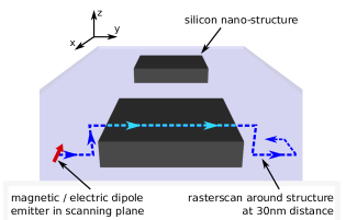
The specific simulation procedure is illustrated in figure 4. We raster-scan a dipolar emitter of either magnetic (, nm) or electric nature (, nm) across a discretized nano-dimer (discretization step nm). The dimer lies in a homogeneous environment of refractive index , corresponding to the optical index of the Gd2O3 film.Dakhel (2001) The distance between emitter and structure is kept at nm. Far from the structure, the dipole is scanned at nm above the substrate. In this way, we account for the distance between the Eu3+-cluster film and the nanostructures due to the 20 nm thick SiO2 layer. With a finite numerical aperture as used in our experiment, we expect that only a very small part of the radiation from dipole emitters oriented along will reach our detector (due to their toroidal radiation pattern propagating perpendicular to the -axis). We show indeed in Appendix IV.2, that a small fraction of contributing -dipoles does not strongly impact on the LDOS maps. Therefore, we will neglect dipole emitters oriented along in the simulations shown in figure 3. Thus, the simulated maps only take into account dipoles located in a plane parallel to the substrate (the computed values being the average of the contributions of dipoles oriented along and ). We denote these average decay rates and for MD and ED, respectively.
The direct result of this procedure has a far too high spatial resolution (see the two columns on the left of figure 3c). Therefore, to account for the diffraction limited size of the laser-spot, and hence the excitation of a whole ensemble of emitters, we convolve the simulated mapping with a Gaussian profile of waist nm (corresponding to a full width at half maximum of around 450 nm which is an upper estimate for the emission area.Wertz et al. (2015); Mack et al. (2017)
Our numerical signal power is described by the following equation:
| (3) |
The integral runs over the area of the laser-spot , is the photon energy of the MD or ED transition, is the density of emitting Eu3+ ions (which we consider homogeneous). is the --averaged decay rate of either a magnetic (“”) or an electric (“”) dipole transition. The exponential factor accounts for the Gaussian intensity profile of the laser beam. The simulated maps after convolution are shown in the right columns of Fig. 3c. We note that a similar procedure has been successfully used to recover the near-field intensity distribution from two-photon luminescence (TPL) measurements on plasmonic nanostructures.Ghenuche et al. (2008)
Discussion
Comparing the simulated and experimental results in figure 3, we observe that the features in the simulated maps are more confined around the dimer blocks. Nevertheless there is a general qualitative agreement. The global features and trends observed in the experimental maps are reproduced by the simulations. The contrasts of electric and/or magnetic LDOS close to dielectric nanostructures are in agreement with recently published experimental results, showing a clear separation of electric and magnetic LDOS above the dielectric structures.Makarov et al. (2018); Sanz-Paz et al. (2018) Also the quantitative trends in the intensity ratios are correctly recovered by the simulations, showing an enhancement of the luminescence intensity by a factor of around 3 for the MD transition and 1.5 in the ED case.
Compared to the simulations, the experimental exhibit broader features. Several effects can contribute to this broadening, first of all, not all emitters are excited at saturation power. The laser spot is of finite, diffraction limited size, hence excites a large collection of emitters at each raster-scan position. Those at the edge of the laser focal spot are excited with a weaker field amplitude, hence not at saturation. Therefore, a residual contribution of the excitation electric field at the laser wavelength cannot be totally neglected. In the LDOS simulations on the other hand, we only take into account a single, saturated point-emitter, raster-scanned across the silicon dimer. To elucidate this effect, we calculate the average electric near-field intensity in the Eu3+ doped film at each laser-spot position, shown in figure 3d for TE polarization (see also Appendix IV.1 for the TM case). In these calculations, we perform a numerical raster-scan with a focused illumination at nm and with a spot size of 300 nm FWHM, corresponding to our experimental configuration. At each position of the focused illumination, we calculate the average total field intensity in the entire Eu3+ doped film. There seems to be a certain resemblance between electric LDOS and excitation field pattern, which makes sense, because the near-field is correlated to the LDOS, even though we compare LDOS and at different wavelengths. The magnetic part of the LDOS on the other hand does not show comparable features. This clear contrast suggests, that close to saturation, the experimental mappings are mainly driven by the electric and magnetic LDOS, while a certain broadening and modification can be explained by a residual contribution of the excitation electric field of the laser. In addition, light might be guided through the dimer when the laser hits one extremity, and Europium ions at the other end, far from the laser spot can be remotely excited in this case as well. Such effect can result in a significant broadening of the spatial features in our mappings,Wertz et al. (2015); Mack et al. (2017) and is not fully taken into account in our current theoretical model, even if an enlarged emission area is considered via the Gaussian convolution.
A better agreement could probably be achieved by simulating an actual “layer” of dipoles, instead of raster-scanning a single emitter, and by taking into account the modified global radiation pattern, since the angular emission of single magnetic and electric dipoles can be strongly affected by the inhomogeneous environmentt.Curto et al. (2013); Colas des Francs et al. (2001); Alaee et al. (2015) However, this would require to consider the excitation intensity as function of the emitter position with respect to the center of the focal spot. A possible approach to the problem of non-saturated emitters could be the description of the Eu3+ emitters in the layer as three-level molecules.Girard et al. (2005); Colas des Francs et al. (2007) These more sophisticated theoretical approaches lie outside the scope of this study and will be the subject of a future work.
III Conclusion
In conclusion, we demonstrated that the enhancement of magnetic and electric dipole transitions is spatially tailored in the near-field of dielectric nanostructures. We obtained our results with a technique which allows the parallel mapping of the electric and magnetic components of the photoluminescence of an Eu3+ doped film in a far-field detection scheme. To this end, a nanometer thin film of rare-earth ion doped clusters is deposited on top of the structures and excited by a tightly focused laser beam. The laser beam is raster-scanned across the structures to obtain D maps of the ED and MD emission enhancement. Numerical simulations of the electric and magnetic LDOS show a general qualitative agreement with the experimental results and provide a good understanding of the underlying physical effects. These results show that the electric and magnetic near-field intensity is confined in distinct regions around simple dielectric nanostructures such as rods or dimers. Our work paves the way towards the very rapid and simple experimental characterization of the response of photonic nanostructures to both, the electric and magnetic field of visible light and towards the design of “on demand” magnetic and electric near-field landscapes by tailoring the resonances (like Mie-type modes, bound states in the continuum) of dielectric nanostructures.He et al. (2018)
IV Appendix – Supplemental Material
IV.1 Excitation field distribution for different laser polarizations
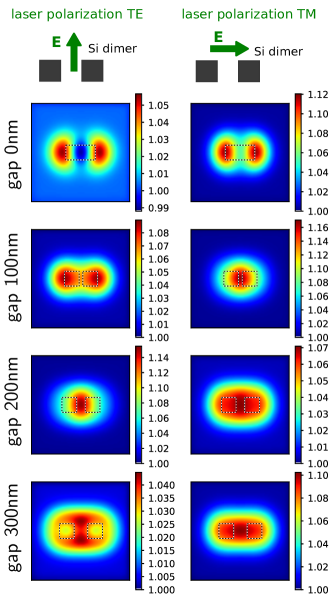
To assess how the excitation field in the europium film depends on the focal position of the laser, we simulated in figure 5 the average electric field intensity induced by the laser-beam, averaged over the whole depot-layer. Each pixel corresponds to the average near-field intensity in the entire film, if the laser is focused at the according position. The left column shows the case of laser light polarized perpendicular to the dimer axis (TE), while the right column depicts the case of a laser polarization along the dimer axis (TM). From top to bottom, increasing gap sizes of nm, nm, nm and nm are shown. Obviously, the field distribution as function of the laser focus position is dependent on the polarization. Together with the observation that the PL-mappings are independent of the laser polarization (see main text figure 2), we conclude that most of the Eu3+ ions in the laser focal spot are excited at saturation.
IV.2 Influence of -oriented dipole transitions
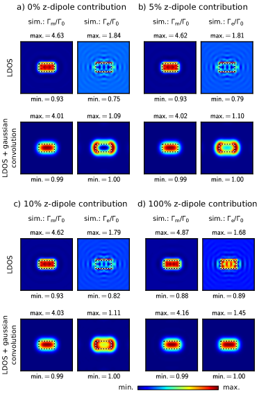
To assess the influence of dipoles along (perpendicular to the scanning plane), we simulated LDOS maps with gradually increased contribution of these emitters. Fig. 6a) shows the LDOS for only and dipole orientations. In b) -dipoles contribute by of their magnitude, in c) by and in d) -dipoles contribute fully. The decay rate of dipoles along experiences the strongest influence through the presence of the dielectric structure, with a very narrow confinement of the LDOS in both cases (for ED and MD). Thus the mappings change significantly, as soon as signal from the perpendicular dipoles is recorded. Hence, we conclude that the dipoles with -orientation are almost invisible in our detection scheme, since their radiation lobe lies in the plane.
IV.3 Background PL
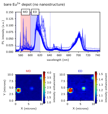
Photoluminescence measurements on the bare film (i.e. in absence of any silicon nanostructures) are shown in figure 7. The PL is very homogeneous over large areas of many microns, with only some defects. These defects do not disturb the measurements, because they are significantly larger than the spatial features obtained from scanning the silicon nanostructures, and therefore can be easily identified.
Acknowledgements.
This work was supported by Programme Investissements d’Avenir under the program ANR-11-IDEX-0002-02, reference ANR-10-LABX-0037-NEXT, by the LAAS-CNRS micro and nanotechnologies platform, a member of the French RENATECH network and by the computing facility center CALMIP of the University of Toulouse under grant P12167.References
- Novotny and Hecht (2006) Lukas Novotny and Bert Hecht, Principles of Nano-Optics (Cambridge University Press, Cambridge ; New York, 2006).
- Giessen and Vogelgesang (2009) Harald Giessen and Ralf Vogelgesang, “Glimpsing the Weak Magnetic Field of Light,” Science 326, 529–530 (2009).
- Pendry (2000) J. B. Pendry, “Negative Refraction Makes a Perfect Lens,” Physical Review Letters 85, 3966–3969 (2000).
- Merlin (2009) Roberto Merlin, “Metamaterials and the Landau–Lifshitz permeability argument: Large permittivity begets high-frequency magnetism,” Proceedings of the National Academy of Sciences 106, 1693–1698 (2009).
- Kuznetsov et al. (2012) Arseniy I. Kuznetsov, Andrey E. Miroshnichenko, Yuan Hsing Fu, JingBo Zhang, and Boris Luk’yanchuk, “Magnetic light,” Scientific Reports 2, 492 (2012).
- Evlyukhin et al. (2012) Andrey B. Evlyukhin, Sergey M. Novikov, Urs Zywietz, René Lynge Eriksen, Carsten Reinhardt, Sergey I. Bozhevolnyi, and Boris N. Chichkov, “Demonstration of Magnetic Dipole Resonances of Dielectric Nanospheres in the Visible Region,” Nano Letters 12, 3749–3755 (2012).
- Kapitanova et al. (2017) Polina Kapitanova, Vladimir Ternovski, Andrey Miroshnichenko, Nikita Pavlov, Pavel Belov, Yuri Kivshar, and Michael Tribelsky, “Giant field enhancement in high-index dielectric subwavelength particles,” Scientific Reports 7, 731 (2017).
- Kuznetsov et al. (2016) Arseniy I. Kuznetsov, Andrey E. Miroshnichenko, Mark L. Brongersma, Yuri S. Kivshar, and Boris Luk’yanchuk, “Optically resonant dielectric nanostructures,” Science 354 (2016), 10.1126/science.aag2472.
- Albella et al. (2014) Pablo Albella, Rodrigo Alcaraz de la Osa, Fernando Moreno, and Stefan A. Maier, “Electric and Magnetic Field Enhancement with Ultralow Heat Radiation Dielectric Nanoantennas: Considerations for Surface-Enhanced Spectroscopies,” ACS Photonics 1, 524–529 (2014).
- Albella et al. (2013) Pablo Albella, M. Ameen Poyli, Mikolaj K. Schmidt, Stefan A. Maier, Fernando Moreno, Juan José Sáenz, and Javier Aizpurua, “Low-Loss Electric and Magnetic Field-Enhanced Spectroscopy with Subwavelength Silicon Dimers,” The Journal of Physical Chemistry C 117, 13573–13584 (2013).
- Rolly et al. (2012) Brice Rolly, Betina Bebey, Sebastien Bidault, Brian Stout, and Nicolas Bonod, “Promoting magnetic dipolar transition in trivalent lanthanide ions with lossless Mie resonances,” Physical Review B 85, 245432 (2012).
- Wiecha et al. (2018) Peter R. Wiecha, Arnaud Arbouet, Aurélien Cuche, Vincent Paillard, and Christian Girard, “Decay rate of magnetic dipoles near nonmagnetic nanostructures,” Physical Review B 97, 085411 (2018).
- Devaux et al. (2000a) Eloıs̈e Devaux, Alain Dereux, Eric Bourillot, Jean-Claude Weeber, Yvon Lacroute, Jean-Pierre Goudonnet, and Christian Girard, “Detection of the optical magnetic field by circular symmetry plasmons,” Applied Surface Science 164, 124–130 (2000a).
- Devaux et al. (2000b) Eloïse Devaux, Alain Dereux, Eric Bourillot, Jean-Claude Weeber, Yvon Lacroute, Jean-Pierre Goudonnet, and Christian Girard, “Local detection of the optical magnetic field in the near zone of dielectric samples,” Physical Review B 62, 10504–10514 (2000b).
- Burresi et al. (2009) M. Burresi, D. van Oosten, T. Kampfrath, H. Schoenmaker, R. Heideman, A. Leinse, and L. Kuipers, “Probing the Magnetic Field of Light at Optical Frequencies,” Science 326, 550–553 (2009).
- Kabakova et al. (2016) I. V. Kabakova, A. de Hoogh, R. E. C. van der Wel, M. Wulf, B. le Feber, and L. Kuipers, “Imaging of electric and magnetic fields near plasmonic nanowires,” Scientific Reports 6 (2016), 10.1038/srep22665.
- Girard et al. (2004) Ch Girard, T David, C Chicanne, A Mary, G. Colas des Francs, E Bourillot, J.-C Weeber, and A Dereux, “Imaging surface photonic states with a circularly polarized tip,” Europhysics Letters (EPL) 68, 797–803 (2004).
- Aigouy et al. (2014) L. Aigouy, A. Cazé, P. Gredin, M. Mortier, and R. Carminati, “Mapping and Quantifying Electric and Magnetic Dipole Luminescence at the Nanoscale,” Physical Review Letters 113, 076101 (2014).
- Carminati et al. (2015) R. Carminati, A. Cazé, D. Cao, F. Peragut, V. Krachmalnicoff, R. Pierrat, and Y. De Wilde, “Electromagnetic density of states in complex plasmonic systems,” Surface Science Reports 70, 1–41 (2015).
- Cuche et al. (2017) A. Cuche, M. Berthel, U. Kumar, G. Colas des Francs, S. Huant, E. Dujardin, C. Girard, and A. Drezet, “Near-field hyperspectral quantum probing of multimodal plasmonic resonators,” Physical Review B 95, 121402 (2017).
- Taminiau et al. (2012) Tim H. Taminiau, Sinan Karaveli, Niek F. van Hulst, and Rashid Zia, “Quantifying the magnetic nature of light emission,” Nature Communications 3, ncomms1984 (2012).
- Carnall et al. (1968) W. T. Carnall, P. R. Fields, and K. Rajnak, “Spectral Intensities of the Trivalent Lanthanides and Actinides in Solution. II. Pm3+, Sm3+, Eu3+, Gd3+, Tb3+, Dy3+, and Ho3+,” The Journal of Chemical Physics 49, 4412–4423 (1968).
- Noginova et al. (2008) N. Noginova, G. Zhu, M. Mavy, and M. A. Noginov, “Magnetic dipole based systems for probing optical magnetism,” Journal of Applied Physics 103, 07E901 (2008).
- Sanz-Paz et al. (2018) Maria Sanz-Paz, Cyrine Ernandes, Juan Uriel Esparza, Geoffrey W. Burr, Niek F. van Hulst, Agnès Maitre, Lionel Aigouy, Thierry Gacoin, Nicolas Bonod, Maria F. Garcia-Parajo, Sébastien Bidault, and Mathieu Mivelle, “Enhancing Magnetic Light Emission with All-Dielectric Optical Nanoantennas,” Nano Letters (2018), 10.1021/acs.nanolett.8b00548.
- Baranov et al. (2017) Denis G. Baranov, Roman S. Savelev, Sergey V. Li, Alexander E. Krasnok, and Andrea Alù, “Modifying magnetic dipole spontaneous emission with nanophotonic structures,” Laser & Photonics Reviews 11, 1600268–n/a (2017).
- Karaveli and Zia (2011) Sinan Karaveli and Rashid Zia, “Spectral Tuning by Selective Enhancement of Electric and Magnetic Dipole Emission,” Physical Review Letters 106, 193004 (2011).
- Hussain et al. (2014) R. Hussain, D. Keene, N. Noginova, and M. Durach, “Spontaneous emission of electric and magnetic dipoles in the vicinity of thin and thick metal,” Optics Express 22, 7744–7755 (2014).
- Choi et al. (2016) Bongseok Choi, Masanobu Iwanaga, Yoshimasa Sugimoto, Kazuaki Sakoda, and Hideki T. Miyazaki, “Selective Plasmonic Enhancement of Electric- and Magnetic-Dipole Radiations of Er Ions,” Nano Letters 16, 5191–5196 (2016).
- Cuche et al. (2009) A. Cuche, B. Masenelli, G. Ledoux, D. Amans, C. Dujardin, Y. Sonnefraud, P. Mélinon, and S. Huant, “Fluorescent oxide nanoparticles adapted to active tips for near-field optics,” Nanotechnology 20, 015603 (2009).
- Guerfi et al. (2013) Y. Guerfi, F. Carcenac, and G. Larrieu, “High resolution HSQ nanopillar arrays with low energy electron beam lithography,” Microelectronic Engineering 110, 173–176 (2013).
- Wiecha et al. (2017) Peter R. Wiecha, Arnaud Arbouet, Christian Girard, Aurélie Lecestre, Guilhem Larrieu, and Vincent Paillard, “Evolutionary multi-objective optimization of colour pixels based on dielectric nanoantennas,” Nature Nanotechnology 12, 163–169 (2017).
- Masenelli et al. (2012) B. Masenelli, G. Ledoux, D. Amans, C. Dujardin, and P. Mélinon, “Shells of crystal field symmetries evidenced in oxide nano-crystals,” Nanotechnology 23, 305706 (2012).
- Perez et al. (2010) A. Perez, P. Melinon, V. Dupuis, L. Bardotti, B. Masenelli, F. Tournus, B. Prevel, J. Tuaillon-Combes, E. Bernstein, A. Tamion, N. Blanc, D. Tainoff, O. Boisron, G. Guiraud, M. Broyer, M. Pellarin, N. Fatti, F. Vallee, E. Cottancin, J. Lerme, J-L. Vialle, C. Bonnet, P. Maioli, A. Crut, C. Clavier, J.l. Rousset, and F. Morfin, “Functional nanostructures from clusters,” International Journal of Nanotechnology 7, 523–574 (2010).
- Murai et al. (2017) S. Murai, M. Saito, H. Sakamoto, M. Yamamoto, R. Kamakura, T. Nakanishi, K. Fujita, M. A. Verschuuren, Y. Hasegawa, and K. Tanaka, “Directional outcoupling of photoluminescence from Eu(III)-complex thin films by plasmonic array,” APL Photonics 2, 026104 (2017).
- Lunnemann and Koenderink (2016) Per Lunnemann and A. Femius Koenderink, “The local density of optical states of a metasurface,” Scientific Reports 6, srep20655 (2016).
- Martin et al. (1995) Olivier J. F. Martin, Christian Girard, and Alain Dereux, “Generalized Field Propagator for Electromagnetic Scattering and Light Confinement,” Physical Review Letters 74, 526–529 (1995).
- Agarwal (1975) G. S. Agarwal, “Quantum electrodynamics in the presence of dielectrics and conductors. I. Electromagnetic-field response functions and black-body fluctuations in finite geometries,” Physical Review A 11, 230–242 (1975).
- Girard et al. (1997) Christian Girard, Jean-Claude Weeber, Alain Dereux, Olivier J. F. Martin, and Jean-Pierre Goudonnet, “Optical magnetic near-field intensities around nanometer-scale surface structures,” Physical Review B 55, 16487–16497 (1997).
- Schröter (2003) U. Schröter, “Modelling of magnetic effects in near-field optics,” The European Physical Journal B 33, 297–310 (2003).
- Sersic et al. (2011) Ivana Sersic, Christelle Tuambilangana, Tobias Kampfrath, and A. Femius Koenderink, “Magnetoelectric point scattering theory for metamaterial scatterers,” Physical Review B 83, 245102 (2011).
- Teulle et al. (2012) Alexandre Teulle, Renaud Marty, Sviatlana Viarbitskaya, Arnaud Arbouet, Erik Dujardin, Christian Girard, and Gérard Colas des Francs, “Scanning optical microscopy modeling in nanoplasmonics,” Journal of the Optical Society of America B 29, 2431 (2012).
- Dakhel (2001) A. A. Dakhel, “Optical constants of evaporated gadolinium oxide,” Journal of Optics A: Pure and Applied Optics 3, 452 (2001).
- Wertz et al. (2015) Esther Wertz, Benjamin P. Isaacoff, Jessica D. Flynn, and Julie S. Biteen, “Single-Molecule Super-Resolution Microscopy Reveals How Light Couples to a Plasmonic Nanoantenna on the Nanometer Scale,” Nano Letters 15, 2662–2670 (2015).
- Mack et al. (2017) David L. Mack, Emiliano Cortés, Vincenzo Giannini, Peter Török, Tyler Roschuk, and Stefan A. Maier, “Decoupling absorption and emission processes in super-resolution localization of emitters in a plasmonic hotspot,” Nature Communications 8, 14513 (2017).
- Ghenuche et al. (2008) Petru Ghenuche, Sudhir Cherukulappurath, Tim H. Taminiau, Niek F. van Hulst, and Romain Quidant, “Spectroscopic Mode Mapping of Resonant Plasmon Nanoantennas,” Physical Review Letters 101, 116805 (2008).
- Makarov et al. (2018) S. V. Makarov, I. S. Sinev, V. A. Milichko, F. E. Komissarenko, D. A. Zuev, E. V. Ushakova, I. S. Mukhin, Y. F. Yu, A. I. Kuznetsov, P. A. Belov, I. V. Iorsh, A. N. Poddubny, A. K. Samusev, and Yu. S. Kivshar, “Nanoscale Generation of White Light for Ultrabroadband Nanospectroscopy,” Nano Letters 18, 535–539 (2018).
- Curto et al. (2013) Alberto G. Curto, Tim H. Taminiau, Giorgio Volpe, Mark P. Kreuzer, Romain Quidant, and Niek F. van Hulst, “Multipolar radiation of quantum emitters with nanowire optical antennas,” Nature Communications 4, 1750 (2013).
- Colas des Francs et al. (2001) Gérard Colas des Francs, Christian Girard, Jean-Claude Weeber, and Alain Dereux, “Relationship between scanning near-field optical images and local density of photonic states,” Chemical Physics Letters 345, 512–516 (2001).
- Alaee et al. (2015) R. Alaee, R. Filter, D. Lehr, F. Lederer, and C. Rockstuhl, “A generalized Kerker condition for highly directive nanoantennas,” Optics Letters 40, 2645–2648 (2015).
- Girard et al. (2005) Christian Girard, Olivier J. F. Martin, Gaëtan Lévèque, Gérard Colas des Francs, and Alain Dereux, “Generalized bloch equations for optical interactions in confined geometries,” Chemical Physics Letters 404, 44–48 (2005).
- Colas des Francs et al. (2007) Gérard Colas des Francs, Christian Girard, Thierry Laroche, Gaëtan Lévèque, and Olivier J. F. Martin, “Theory of molecular excitation and relaxation near a plasmonic device,” The Journal of Chemical Physics 127, 034701 (2007).
- He et al. (2018) Yuan He, Guangtao Guo, Tianhua Feng, Yi Xu, and Andrey E. Miroshnichenko, “Toroidal dipole bound states in the continuum,” Physical Review B 98, 161112 (2018).