Realization of a double-slit SQUID geometry by Fermi arc surface states in a WTe2 Weyl semimetal.
Abstract
We experimentally study electron transport between two superconducting indium leads, coupled to the WTe2 crystal surface. WTe2 is characterized by presence of Fermi arc surface states, as a predicted type-II Weyl semimetal candidate. We demonstrate Josephson current in unprecedentedly long 5 m In-WTe2-In junctions, which is confirmed by curves evolution with temperature and magnetic field. The Josephson current is mostly carried by the topological surface states, which we demonstrate in a double-slit SQUID geometry, realized by coupling the opposite WTe2 crystal surfaces.
pacs:
73.40.Qv 71.30.+hI Introduction
Recent renewal of interest to semimetals is mostly connected with topological effects. Weyl semimetals are conductors whose low-energy bulk excitations are Weyl fermions armitage . Like other topological materials hasan ; zhang ; das ; chiu , Weyl semimetals are characterized by topologically protected metallic surface states, which are known as Fermi arc surface states. This concept of the Fermi arc surface states has now been extended to type II materials armitage , like MoTe2 and WTe2, which contain electron and hole pockets deng ; wang . The non-trivial properties of these materials have been demonstrated in magnetotransport experiments mazhar ; wang-miao .
Topological materials exhibit non-trivial physics in proximity with a superconductor ingasb ; nbsemi ; nbhgte . For the topological insulators zhang1 ; kane ; zhang2 , it is expected to allow topological superconductivity regime Fu ; yakoby , which stimulates a search for Majorana fermions reviews . In the case of Weyl semimetals, the proximity is predicted spec to produce specular Andreev reflection been1 ; been2 , or even to superconducting correlations within a semimetal corr1 ; corr2 ; corr3 . Moreover, topological transport is responsible for Josephson current in 1-2 m long superconductor-normal-superconductor (SNS) junctions in graphene calado ; borzenets .
The edge current contribution can be retrieved even for systems with conducting bulk by analyzing Josephson current suppression in low magnetic fields yakoby ; kowen . The maximum supercurrent is periodically modulated, with period which is defined by the magnetic flux quantum . It is well known, that the homogeneous supercurrent density in the conductor corresponds to a single-slit Fraunhofer pattern tinkham . As the edge currents emerge in a two-dimensional topological system, the sinusoidal oscillation pattern appears yakoby ; kowen , which is a fingerprint of a superconducting quantum interference device (SQUID) tinkham . It is therefore reasonable to study Josephson current suppression in a long SNS junction on a three-dimensional Weyl semimetal surface.
Here, we experimentally study electron transport between two superconducting indium leads, coupled to the WTe2 crystal surface. WTe2 is characterized by presence of Fermi arc surface states, as a predicted type-II Weyl semimetal candidate. We demonstrate Josephson current in unprecedentedly long 5 m In-WTe2-In junctions, which is confirmed by curves evolution with temperature and magnetic field. The Josephson current is mostly carried by the topological surface states, which we demonstrate in a double-slit SQUID geometry, realized by coupling the opposite WTe2 crystal surfaces.
II Samples and technique

WTe2 compound was synthesized from elements by reaction of metal with tellurium vapor in the sealed silica ampule. The WTe2 crystals were grown by the two-stage iodine transport growth1 , that previously was successfully applied growth1 ; growth2 for growth of other metal chalcogenides like NbS2 and CrNb3S6. The WTe2 composition is verified by energy-dispersive X-ray spectroscopy. The X-ray diffraction (Oxford diffraction Gemini-A, MoK) confirms orthorhombic single crystal WTe2 with lattice parameters Å, Å, and Å. We check by standard magnetoresistance measurements that our WTe2 crystals demonstrate large, non-saturating positive magnetoresistance up to 14 T field, as it has been shown for WTe2 Weyl semimetal mazhar .
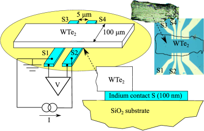
A sample sketch is presented in Fig. 1. Superconducting leads are formed by lift-off technique after thermal evaporation of 100 nm indium on the insulating SiO2 substrate. A WTe2 single crystal ( dimensions) is weakly pressed to the indium leads pattern, so that planar In-WTe2 junctions () are formed at the bottom surface of the crystal WTe2 in Fig. 1.
Charge transport is investigated between two superconducting indium leads in a four-point technique. An example of electrical connections is presented in Fig. 1 : the S1 electrode is grounded; a current is fed through the S2; a voltage drop is measured between these S1 and S2 electrodes by independent wires. In this connection scheme, all the wire resistances are excluded, which is necessary for low-impedance In-WTe2-In junctions (below 0.5 Ohm normal resistance in the present experiment). The measurements are performed in standard He4 cryostat in the temperature range 1.4 K – 4.2 K. The indium leads are superconducting below the critical temperature indium .
III Experimental results

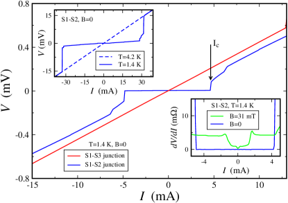
To obtain characteristics, we sweep the dc current and measure the voltage drop . Fig. 2 presents examples in two different experimental configurations.
In zero magnetic field, at low temperature 1.4 K, transport between two 5 m spaced contacts S1 and S2 is of clear Josephson-like behavior tinkham , as shown by the blue curve in Fig. 2: (i) by the four-point connection scheme we directly demonstrate zero resistance region at low currents; (ii) the non-zero resistance appears as sharp jumps at current values mA. The jump positions are subjected to small hysteresis with the sweep direction, so they are slightly different for two branches in Fig. 2. Because of similar preparation technique, different samples demonstrate even quantitatively similar behavior: the obtained values differ within 10% of magnitude for different samples and in different coolings. In contrast, the resistance is always finite between 80 m separated S1 and S3 indium leads, see the red curve in Fig. 2.
Even for the closely-spaced contacts S1 and S2, curve can be switched to standard Ohmic behavior, if the indium superconductivity is suppressed by temperature or high current (above mA for the present dimensions), as depicted in the left inset to Fig. 2. The zero-resistance state can also be suppressed by magnetic field, as it is demonstrated in the right inset to Fig. 2.
Thus, we demonstrate in Fig. 2, that two superconducting contacts induce Josephson current in an unprecedentedly long 5 m In-WTe2-In junction, where nm is the indium correlation length indium .
As usual for SNS junctions, an important information can be obtained from the maximum supercurrent suppression by temperature and magnetic field. To analyze behavior, we use characteristics like ones presented in the right inset to Fig. 2: the dc current is additionally modulated by a low ac component (100 nA, 10 kHz), an ac part of () is detected by a lock-in amplifier. We have checked, that the lock-in signal is independent of the modulation frequency in the 6 kHz – 30 kHz range, which is defined by applied ac filters. To obtain values with high accuracy for given values, we sweep current ten times from zero (superconducting state) to above (resistive state), and then determine as the average value of jump positions in different sweeps.

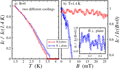
The results are presented in Fig. 3. monotonously falls to zero at 3.5 K, which well corresponds to the indium critical temperature indium , see Fig. 3 (a). However, does not demonstrate the exponential decay, which is expected kulik-long for long SNS junctions. Instead, the experimental dependence is even slower than the linear function of in Fig. 3 (a), as it is usually realized for the short junction regime kulik-long .
To our surprize, suppression pattern crucially depends on the magnetic field orientation to the In-WTe2-In junction plane, see Fig. 3 (b). If the magnetic field is perpendicular to the plane, strong suppression of is observed, which is usual for standard Josephson effect tinkham . In contrast, is diminishing very slowly (within 10% until the indium critical field) for the parallel magnetic field. For both orientations, we observe equidistant oscillations within 5% of magnitude, see also inset to Fig. 3 (b). The oscillations are characterized by high mT period for the parallel field and by low mT for the perpendicular one. It can be easily seen, that the observed supression in parallel magnetic fields resembles double-slit SQUID behavior yakoby ; kowen , so the surface transport is important in WTe2.
IV Discussion
The experimental dependencies allows us to unambiguously identify the topological effects.
Slow decay has been reported in long 1.5-2 m SNS junctions on graphene, and has been connected with topological transport calado ; borzenets . WTe2 is regarded as type-II Weyl semimetal wang ; mazhar ; wang-miao , which contains topological Fermi arc surface states. These surface states are usually decoupled from the bulk hofman ; osbite . On the other hand, Weyl surface states inherit the chiral property of the Chern insulator edge states armitage . Because of topological protection, they can efficiently transfer the Josephson current. This might be a reason calado ; borzenets to have slow dependence kulik-short in our nominally long nm devices.

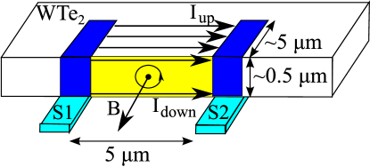
We should connect behavior with the distribution of the Josephson current within the WTe2 crystal, see Fig. 4. The sample thickness is comparable with indium coherence length nm, so the regions of proximity-induced superconductivity couples two opposite sample surfaces near the In leads (blue regions in Fig. 4). The Josephson current is transferred by topological surface states, so there are two parallel weak links between the superconducting leads. In other words, a non-symmetric double-slit SQUID geometry yakoby ; kowen is realized, see Fig. 4.
The experimental suppression pattern well corresponds to the double-slit SQUID yakoby ; kowen with two non-equivalent weak links. Parallel magnetic field induces a phase shift between the opposite WTe2 surfaces, so it controls the magnetic flux through the effective SQUID area, see Fig. 4. The latter can be estimated () from mT as , which gives 0.3m sample thickness for our 5 m long junctions. This estimation is in good correspondence with the known WTe2 crystal thickness.
If the magnetic field is perpendicular to the WTe2 crystal plane, there is no phase shift between the the opposite sample surfaces. Instead, reflects homogeneous supercurrent distribution within the surface state in two equivalent SNS junctions. Thus, we observe strong suppression in Fig. 3 (b) with oscillations in low fields tinkham , which reflects the effective junction area . The experimentally observed period mT in the inset to Fig. 3 (b) corresponds to , i.e. to the 5 m m SNS junctions, which well correspond to the sample dimensions.
V Conclusion
As a conclusion, we experimentally study electron transport between two superconducting indium leads, coupled to the WTe2 crystal surface. WTe2 is characterized by presence of Fermi arc surface states, as a predicted type-II Weyl semimetal candidate. We demonstrate Josephson current in unprecedentedly long 5 m In-WTe2-In junctions, which is confirmed by curves evolution with temperature and magnetic field. The Josephson current is mostly carried by the topological surface states, which we demonstrate in a double-slit SQUID geometry, realized by coupling the opposite WTe2 crystal surfaces.
Acknowledgements.
We wish to thank Ya. Fominov, V.T. Dolgopolov, V.A. Volkov for fruitful discussions, and S.S Khasanov for X-ray sample characterization. We gratefully acknowledge financial support by the RFBR (project No. 16-02-00405) and RAS.References
- (1) As a recent review see N. P. Armitage, E. J. Mele, and Ashvin Vishwanath, Reviews of Modern Physics (2017), arxiv:1705.01111
- (2) M. Z. Hasan and C. L. Kane, Rev. Mod. Phys. 82, 3045 (2010).
- (3) X.-L. Qi and S.-C. Zhang, Rev. Mod. Phys. 83, 1057 (2011).
- (4) A. Bansil, H. Lin, and T. Das, Rev. Mod. Phys. 88, 021004 (2016).
- (5) C.-K. Chiu, J. C. Teo, A. P. Schnyder, and S. Ryu, Rev. Mod. Phys. 88, 035005 (2016).
- (6) Deng K., Wan G., Deng P., Zhang K., Ding S., Wang E., Yan M., Huang H., Zhang H., Xu Z., Denlinger J., Fedorov A., Yang H., Duan W., Yao H., Wu Y., Fan S., Zhang H., Chen X., Zhou S., Nat. Phys. 12, 1105–1110 (2016).
- (7) Chenlu Wang et al., Phys. Rev. B 94, 241119(R)
- (8) Mazhar N. Ali, Jun Xiong, Steven Flynn, Jing Tao, Quinn D. Gibson, Leslie M. Schoop, Tian Liang, Neel Haldolaarachchige, Max Hirschberger, N. P. Ong and R. J. Cava Nature 514, 205 (2014). doi:10.1038/nature13763
- (9) Wang, Y. et al., Nat. Commun. 7, 13142 (2016). doi: 10.1038/ncomms13142
- (10) A. Kononov, V.A. Kostarev, B.R. Semyagin, V.V. Preobrazhenskii, M.A. Putyato, E.A. Emelyanov, and E.V. Deviatov, Physical Review B 96, 245304 (2017). DOI: 10.1103/PhysRevB.96.245304
- (11) A. Kononov, S. V. Egorov, Z. D. Kvon, N. N. Mikhailov, S. A. Dvoretsky, and E. V. Deviatov, Phys. Rev. B 93, 041303(R) (2016)
- (12) A. Kononov, S. V. Egorov, N. Titova, Z. D. Kvon, N. N. Mikhailov, S. A. Dvoretsky, E. V. Deviatov, JETP Lett., 101 , 41 (2015).
- (13) S. Murakami, N. Nagaosa, S.-C. Zhang, Phys. Rev. Lett. 93, 156804 (2004).
- (14) C. L. Kane, E. J. Mele, Phys. Rev. Lett. 95, 146802 (2005).
- (15) B. A. Bernevig, S.-C. Zhang, Phys. Rev. Lett. 96, 106802 (2006).
- (16) L. Fu and C. L. Kane, Phys. Rev. Lett. 100, 96407 (2008).
- (17) S. Hart, H. Ren, T. Wagner, Ph. Leubner, M. Mühlbauer, C. Brüne, H. Buhmann, L. W. Molenkamp and A. Yacoby, Nature Physics 10, 638–643 (2014).
- (18) For recent reviews, see C. W. J. Beenakker, Annu. Rev. Con. Mat. Phys. 4, 113 (2013) and J. Alicea, Rep. Prog. Phys. 75, 076501 (2012).
- (19) Wei Chen, Liang Jiang, R. Shen, L. Sheng, B. G. Wang, D. Y. Xing EPL 103, 27006 (2013)
- (20) C. W. J. Beenakker, Physical Review Letters 97 (2006).
- (21) C. W. J. Beenakker, Reviews of Modern Physics 80, 1337 (2008).
- (22) T. Meng and L. Balents, Phys. Rev. B 86, 054504 (2012).
- (23) G. Y. Cho, J. H. Bardarson, Y.-M. Lu, and J. E. Moore, Phys. Rev. B 86, 214514 (2012).
- (24) H. Wei, S. P. Chao, and V. Aji, Phys. Rev. B 89, 014506 (2014).
- (25) V. E. Calado, S. Goswami, G. Nanda, M. Diez, A. R. Akhmerov, K. Watanabe, T. Taniguchi, T. M. Klapwijk & L. M. K. Vandersypen, Nature Nanotechnology 10, 761–764 (2015). doi:10.1038/nnano.2015.156
- (26) I.V. Borzenets, F. Amet, C.T. Ke, A.W. Draelos, M.T. Wei, A. Seredinski, K. Watanabe, T. Taniguchi, Y. Bomze, M. Yamamoto, S. Tarucha, and G. Finkelstein, Phys. Rev. Lett. 117, 237002 (2016), http://dx.doi.org/10.1103/PhysRevLett.117.237002
- (27) Sean Hart, Hechen Ren, Timo Wagner, Philipp Leubner, Mathias Mühlbauer, Christoph Brüne, Hartmut Buhmann, Laurens W. Molenkamp & Amir Yacoby, Nature Physics 10, 638–643 (2014), doi:10.1038/nphys3036
- (28) Vlad S. Pribiag, Arjan J. A. Beukman, Fanming Qu, Maja C. Cassidy, Christophe Charpentier, Werner Wegscheider & Leo P. Kouwenhoven, Nature Nanotechnology 10, 593 (2015)
- (29) M. Tinkham, Introduction to Superconductivity (2d ed., McGraw–Hill, New York, 1996).
- (30) E. B. Borisenko, V. A. Berezin, N. N. Kolesnikov, V. K. Gartman, D. V. Matveev, O. F. Shakhlevich, Physics of the Solid State, 59, 1310, (2017).
- (31) A. Sidorov, A.E. Petrova, A.N. Pinyagin, N.N. Kolesnikov, S.S. Khasanov, S.M. Stishov, JETP, 122, 1047, (2016).
- (32) A. M. Toxen Phys. Rev. 123, 442 (1961).
- (33) I.O. Kulik and A.N. Omelyanchuk, Fiz. Nizk. Temp. 3, 945 (1977) [Sov. J. Low Temp. Phys. 3, 459 (1977)].
- (34) I. O. Kulik, Sov. Phys. JETP 30, 944 (1970).
- (35) Marco Bianchi, Richard C. Hatch, Jianli Mi, Bo Brummerstedt Iversen, and Philip Hofmann, Phys. Rev. Lett. 107, 086802 (2011)
- (36) O.O. Shvetsov, V.A. Kostarev, A. Kononov, V.A. Golyashov, K.A. Kokh, O.E. Tereshchenko, and E.V. Deviatov, EPL 119, 57009 (2017), doi:10.1209/0295-5075/119/57009