Voltage-driven Building Block for Hardware Belief Networks
Abstract
Probabilistic spin logic (PSL) based on networks of binary stochastic neurons (or -bits) has been shown to provide a viable framework for many functionalities including Ising computing, Bayesian inference, invertible Boolean logic and image recognition. This paper presents a hardware building block for the PSL architecture, consisting of an embedded MTJ and a capacitive voltage adder of the type used in neuMOS. We use SPICE simulations to show how identical copies of these building blocks (or weighted -bits) can be interconnected with wires to design and solve a small instance of the NP-complete Subset Sum Problem fully in hardware.
Keywords - Probabilistic computing, Embedded MTJ, -bits, -circuits, Invertible Boolean logic, Subset Sum Problem
I Introduction
Probabilistic spin logic (PSL) has been shown to provide a viable framework for Ising computing Sutton et al. (2017); Behin-Aein et al. (2016); Shim et al. (2017), Bayesian inference Behin-Aein et al. (2016), invertible Boolean logic Camsari et al. (2017a), and image recognition Zand et al. (2017). The PSL model is defined by two equations Camsari et al. (2017a) loosely analogous to a neuron and a synapse. The former is what we call the -bit whose output is related to its dimensionless input by the relation
| (1a) |
where rand(1,+1) is a random number uniformly distributed between 1 and +1, and is the normalized time unit. The synapse generates the input from a weighted sum of the states of other -bits according to the relation
| (1b) |
where, is the on-site bias and is the weight of the coupling from -bit to -bit and is a dimensionless constant. These two equations constitute the behavioral model of PSL. The objective of this paper is to present a voltage-driven hardware building block using present day device technologies such as embedded MRAM Lin et al. (2009) and Floating-Gate MOS transistors, such that identical copies of the same block can be interconnected with wires to implement Eqs. 1b.
The paper is organized as follows: We first show a complete hardware mapping for the weighted -bit by augmenting a recently introduced Magnetoresistive Random Access Memory (MRAM) type stochastic unit Camsari et al. (2017b) with a floating gate MOS-based capacitive network Shibata and Ohmi (1992). We then show how the results of a fully interconnected -bit circuit closely approximate the the ideal equations using an example of an “invertible” Full Adder that can perform 1-bit addition and subtraction. Finally, we show how such invertible Full Adders can be interconnected to solve a simple instance of the NP-complete Subset Sum Problem.
Each example in this paper has been obtained using full SPICE models which simply uses transistors, capacitors and resistors without any additional complex circuitry or processing.
II Building block
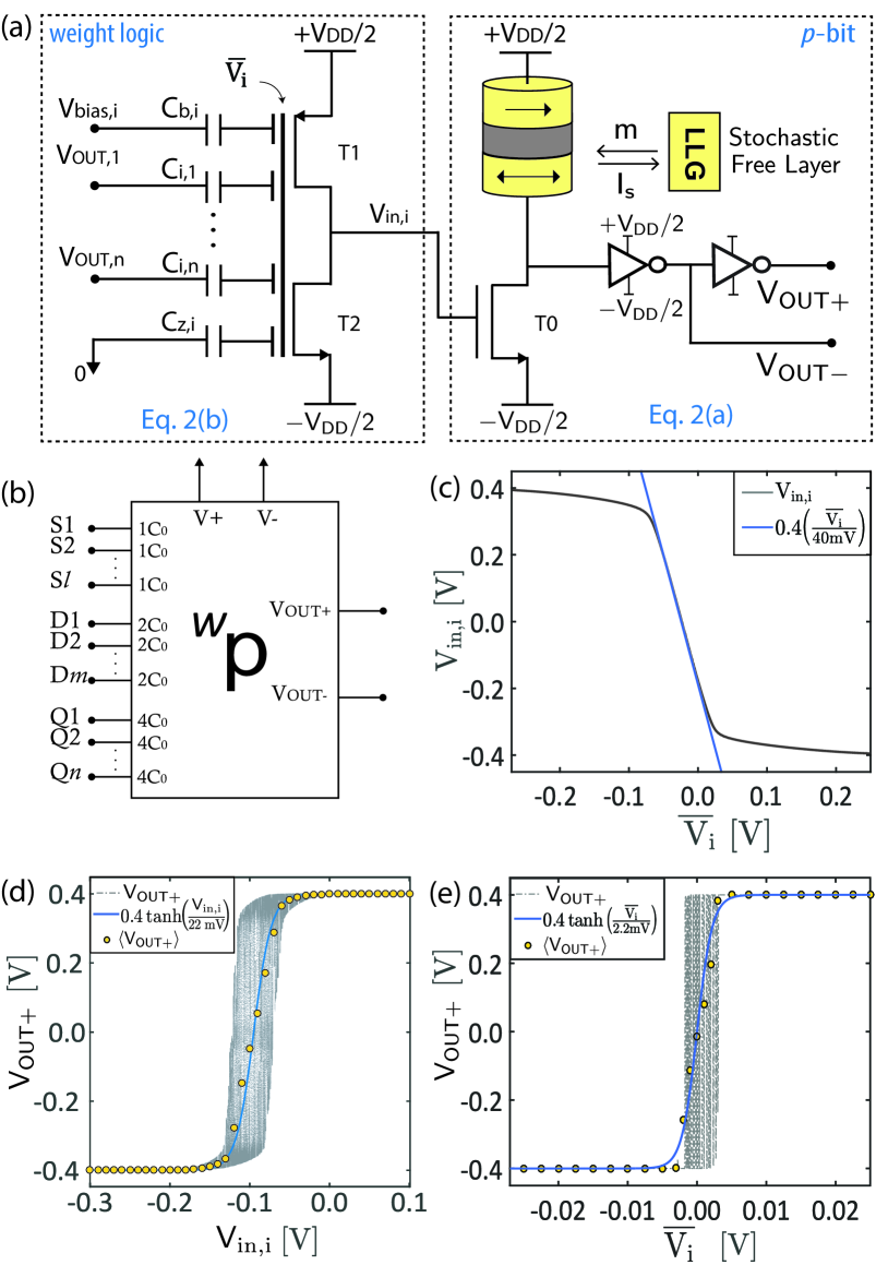
Our building block has two components corresponding to the two Eqs. 1ba,b. Eq. 1ba is implemented by the -bit in Fig.1a which consists of an embedded low-barrier unstable MTJ coupled to two CMOS inverters which provides a stochastic output whose average value is controlled by the input voltage:
| (2a) | |||
| where are the supply voltages, and is a parameter () describing the width of the sigmoidal response. | |||
The value of depends on the details of the 1T/1MTJ in the embedded MRAM structure Camsari et al. (2017b) and the transistor characteristics. The conductance, of the MTJ is chosen to match the MTJ switching characteristics to the transistors in the -bit so that the overall transfer characteristics is centered at zero as shown in Fig. 1e. To do that, an input voltage of 0V is applied at the input of T1 and T2 transistors turning both of them ON () and is swept to observe the outputs. The value for which = is the value chosen to be the MTJ conductance. For minimum sized 14nm HP-FinFET transistors models with , 62 k and it seems reasonable considering the RA-products of modern MTJs Mizrahi (2018).
Eqs. 1bb is implemented by the weighted synapse portion of Fig. 1a , which is a capacitive voltage adder just like those used in neuMOS devices Shibata and Ohmi (1992); Nakamura et al. (2015). We can write
| (2b) |
Note that the capacitive voltage divider typically attenuates the voltage at its output, and the inverter scales it up to as shown in Fig. 1c, the two being related approximately by
| (2c) |
where is a parameter characteristic of the inverter. Eqs. 2ca,b can be mapped onto the PSL Eqs. 1ba,b by defining
| (3a) | |||
| (3b) | |||
| (3c) | |||
| (3d) |
is the intrinsic gate capacitance of the neuMOS inverter. The significance of is that we assume the input is composed of many identical capacitors , and that the weights have been designed to have integer values such that can be implemented by connecting elementary capacitors in parallel. The other coefficients , are also integers. We adjust the number of bias capacitors to facilitate external biasing and the number of grounded capacitors to make a constant, so that is independent of index :
| (4) |
Note that is usually a fairly large number equal to the sum of all the weights, and to implement an it is important to keep the factor to be much greater than 1. This is the reason for using an inverter between the capacitive voltage adder and the -bit. Our model neglects any leakage resistances associated with the capacitive weights. Modern transistors with thin oxides can have gate leakage currents 1nA, with RC s-ms. This should not affect the weighting, since the examples presented here operate at sub-ns time scales. For slower neurons, it may be advisable to use thicker oxides for the capacitive weights to ensure lower leakage.
Fig. 1b shows the icon we use to represent our building block which we call a weighted -bit. The input consists of three types of inputs designated S, D and Q having capacitances , and . Combinations of these are used to implement different weights and different bias . Each block has two outputs . The choice of output depends on the sign of the corresponding . Similarly different signs of are implemented by choosing to be or .
III Invertible full adder
In PSL, any given truth table can be implemented using Eq. 1b by choosing an appropriate and matrices Camsari et al. (2017a). Here we show how those and are mapped onto physical hardware using our proposed building block using only transistors, resistors and capacitances.
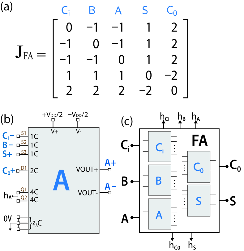
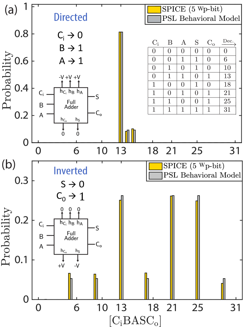
A Full Adder can be implemented in PSL using the matrix shown in Fig. 2. In this paper, we improve the 14 -bit implementation of the invertible Full Adder (FA) in Ref.Camsari et al. (2017a) and implement the same functionality using 5 -bits. This is achieved by first noting that the first half of the FA truth table is complementary to the second half for the FA (Fig. 3a inset). The first 4 lines in the truth table is turned into an orthonormal set by a Gram-Schmidt process and a [J] matrix is obtained using Eq.12 in Ref.Camsari et al. (2017a) which is finally rounded to integer values, with diagonal entries replaced by zeros. This defines the interconnection between the 5 -bits of the Full Adder in hardware. Each row of the matrix are realized in terms of capacitive coupling to the gate of the associated terminal.
To ensure a uniform is applied to each -bit (Eq. 4), the same weighting factor K needs to be used for all -bits. To apply a given , we first find max() for any given , and then ground ( unit capacitances for all terminals where is a number that can be used to control , a larger causing a smaller . Fig. 2b shows explicit connections made to one of the inputs “A” and Fig. 2c shows the subcircuit of the Full Adder with as inputs, as the outputs, and as the clamping pins.
Fig. 4 shows the operation of a Full Adder in the usual forward mode with clamped to values (0,1,1) which forces the to (0,1) according to the truth table. In the invertible mode are clamped to (0,1) and the circuit stochastically searches consistent combinations of to satisfy the truth table: . Fig. 4 shows steady state (t = 1 ) histogram plots of the Full Adder operation in direct and inverted mode side by side with results from the PSL behavioral model.
The good agreement between the ideal PSL behavioral model and the coupled SPICE simulation that solves PTM-based transistors models with stochastic LLG validates the hardware mapping of the ideal -bit equations with the weighted -bits.
IV 3SUM Problem
3SUM is a decision problem in complexity theory that asks whether three elements of a given set can sum up to zero. A variant of the problem is when the set of three numbers have to add up to a given constant number. This problem has a polynomial time solution and is not in NP. In this section, we show how the invertibility feature of the Full Adders can be utilized to design a hardware 3SUM solver, and in the next section, we show how the 3SUM hardware can be modified to design a general solver for the NP-complete Subset Sum Problem.
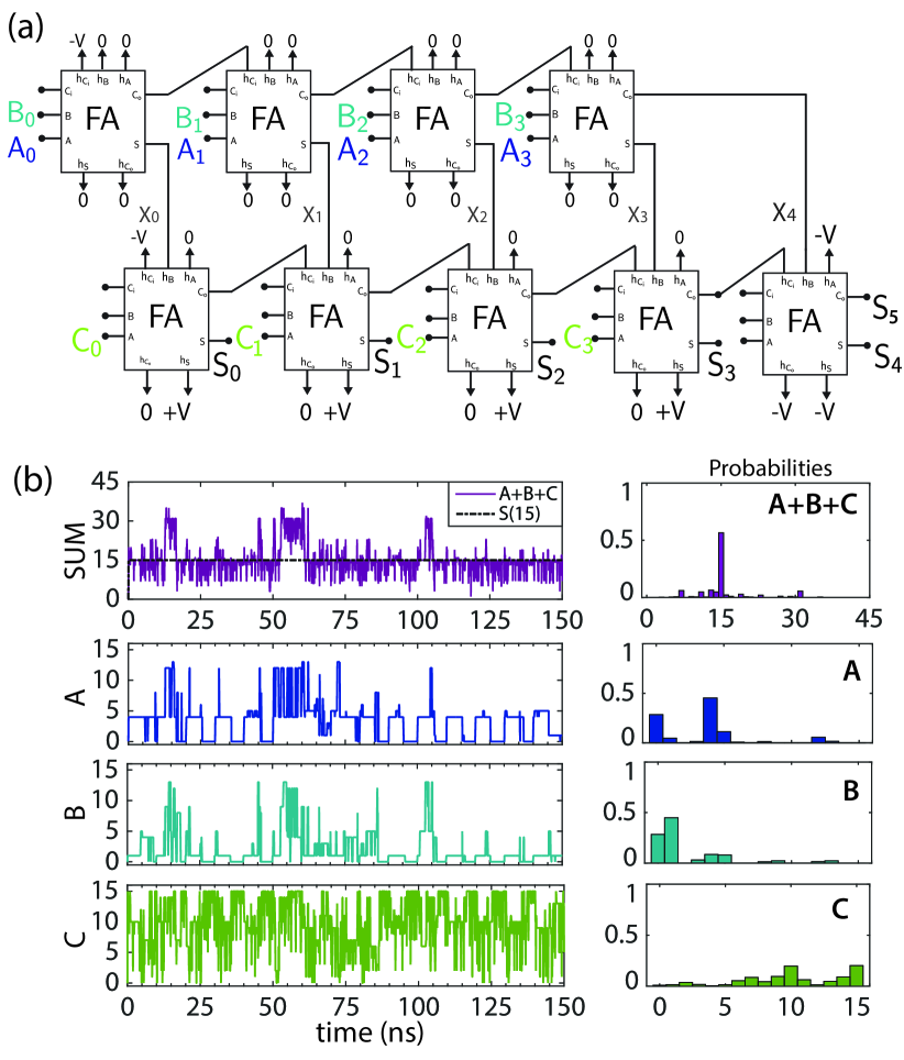
The invertibility property of the Full Adders ensure that given the sum, it can provide the possible input combinations for that sum as shown in Fig.4a. So an n-bit 3 number adder circuit implemented in PSL can essentially provide solution sets for the 3SUM problem when the sum is clamped to a given value.
Fig. 4a shows the circuit constructed out of Full Adders to solve a 4-bit 3SUM problem. Each of the Full Adders in the circuit are the 5 -bit invertible adders that were shown in Fig. 3. The first row of adders adds the two 4-bit numbers A and B, and feeds its output X, to the next row of adders which adds X and C to give the sum . Because -circuits are invertible, if we clamp the sum S, the circuit naturally explores through all possible sets and multisets of the set of all integers from 0 to that add up to S. The given set for the problem could be implemented through clamping certain bits of A,B and C or externally circuitry could be used to detect only the results that belong to the given set. Fig. 4b shows the how A,B,C is fluctuating between values that satisfy the clamped sum 15.
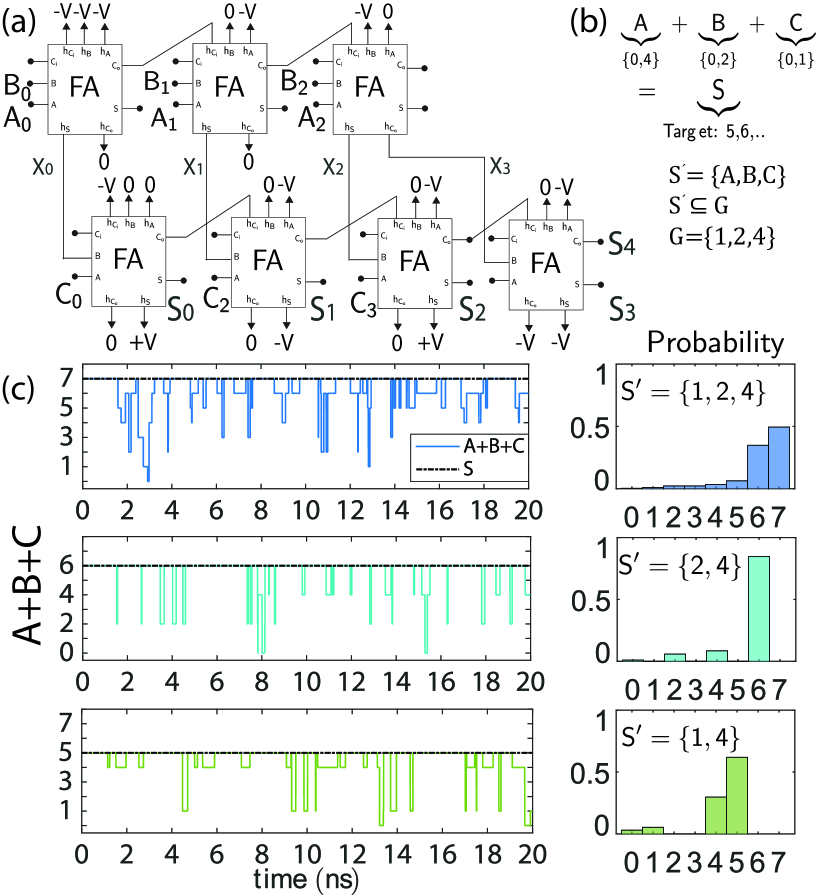
V Subset-sum Problem (SSP)
In this section, we show how the hardware circuit that was designed for 3SUM problem could be modified to solve a small instance of subset-sum problem (SSP) Cormen (2009) which is believed to be a fundamentally difficult problem in computer science (NP-complete). The SSP asks, given a set G with a finite number of positive numbers, if there is a subset S’ such that S’ G whose elements sum to a specified target. For example, Fig. 5 shows a circuit that is programmed to choose a set, G= and a target that is defined by 4-bits. In the 3SUM circuit the input bits (A, B, C) were left “floating”, here, the inputs are constrained to a given number (1,2,4) by clamping the remaining bits of an input. For example, the inputs and are clamped to zero to make A either 4 or 0. Under these conditions, clamping the output to a specified target makes the circuit search for a consistent input combination to find a subset that satisfies the clamped target. Fig. 5c shows three example targets where the inputs get correlated to satisfy the clamped sum. The invertibility feature that is utilized to solve the SSP in this hardware is similar to those discussed in the context of memcomputing Traversa and Di Ventra (2017), however the physical mechanisms are completely different.
One striking difference in the design of the SSP we considered, compared to the 3SUM hardware is the direction of information. In 3SUM the connections were from the first layer of Full Adders to the second, as in normal addition (Fig. 4a). In the SSP, we observed that reversing these connections from the second layer of adder to the first layer drastically improves the accuracy of the solution (Fig. 5a). A similar observation regarding the directional flow of information for another inverse problem using -circuits (integer factorization) was made in Camsari et al. (2017a). Here we have limited the discussion to a small instance of the SSP which would in general require more layers of Full Adders in both vertical and horizontal directions to account for more numbers of elements in G and their size. The purpose of this example is to illustrate how invertibility can be combined with standard digital VLSI design to construct any general “cost function” for hard problems of computer science in an asynchronously running hardware platform without any external clocking.
VI Conclusion
In this paper we have proposed a compact building-block for Probabilistic Spin Logic (PSL) combining a recently proposed Embedded MRAM-based -bit, with an integrated capacitive network that can be implemented using Floating Gate MOS (FGMOS) transistors similar to the neuMOS concept. We have shown by extensive SPICE simulations that the results of the hardware model for the weighted -bit agree well with the behavioral equations of PSL. Having dedicated MTJ based hardware stochastic neurons could help minimize the footprint and consume lower power for applications as also indicated by ref.Zand et al. (2017); Mizrahi (2018). Even though an FGMOS-based capacitive network for performing the voltage addition seems like a natural option, we note that the device equations for any capacitance [] or conductance network [ would have been essentially the same. Moreover, our discussion was only about static weights, but an FPGA-like reconfigurable weighting scheme can also be employed either by using transistor-based gates or by additional multiplexing circuitry to perform online learning or to redesign -circuit connectivity. Finally, using the basic building block we have shown how a small instance of the NP-complete Subset Sum Problem hardware solver can be designed using the unique invertibility feature of -circuits.
Acknowledgment
This work was supported in part by the Center for Probabilistic Spin Logic for Low-Energy Boolean and Non-Boolean Computing (CAPSL), one of the Nanoelectronic Computing Research (nCORE) Centers as task 2759.005, a Semiconductor Research Corporation (SRC) program sponsored by the NSF through ECCS 1739635.
References
- Sutton et al. (2017) B. Sutton, K. Y. Camsari, B. Behin-Aein, and S. Datta, Scientific Reports 7 (2017).
- Behin-Aein et al. (2016) B. Behin-Aein, V. Diep, and S. Datta, Scientific reports 6 (2016).
- Shim et al. (2017) Y. Shim, A. Jaiswal, and K. Roy, Journal of Applied Physics 121, 193902 (2017), http://dx.doi.org/10.1063/1.4983636 .
- Camsari et al. (2017a) K. Y. Camsari, R. Faria, B. M. Sutton, and S. Datta, Phys. Rev. X 7, 031014 (2017a).
- Zand et al. (2017) R. Zand, K. Y. Camsari, I. Ahmed, S. D. Pyle, C. H. Kim, S. Datta, and R. F. DeMara, arXiv preprint arXiv:1710.00249 (2017).
- Lin et al. (2009) C. Lin, S. Kang, Y. Wang, K. Lee, X. Zhu, W. Chen, X. Li, W. Hsu, Y. Kao, M. Liu, et al., Electron Devices Meeting (IEDM), 2009 IEEE International (IEEE, 2009) pp. 1–4.
- Camsari et al. (2017b) K. Y. Camsari, S. Salahuddin, and S. Datta, IEEE Electron Device Letters 38, 1767 (2017b).
- Shibata and Ohmi (1992) T. Shibata and T. Ohmi, IEEE Transactions on Electron devices 39, 1444 (1992).
- Mizrahi (2018) A. Mizrahi, T. Hirtzlin, A. Fukushima, K. Hitoshi, Y. Shinji, J. Grollier and D. Querlioz, Neural-like computing with populations of superparamagnetic basis functions Nature communications,9, 1533 (2018).
- Nakamura et al. (2015) N. Nakamura, K. Shimada, T. Matsuda, and M. Kimura, Future of Electron Devices, Kansai (IMFEDK), 2015 IEEE International Meeting for (IEEE, 2015) pp. 90–91.
- Cormen (2009) T. H. Cormen, Introduction to algorithms (MIT press, 2009).
- Traversa and Di Ventra (2017) F. L. Traversa and M. Di Ventra, Chaos: An Interdisciplinary Journal of Nonlinear Science 27, 023107 (2017).