Flat-band localization and self-collimation of light in photonic crystals
Abstract
We investigate the optical properties of a photonic crystal composed of a quasi-one-dimensional flat-band lattice array through finite-difference time-domain simulations. The photonic bands contain flat bands (FBs) at specific frequencies, which correspond to compact localized states as a consequence of destructive interference. The FBs are shown to be nondispersive along the line, but dispersive along the line. The FB localization of light in a single direction only results in a self-collimation of light propagation throughout the photonic crystal at the FB frequency.
keywords:
Photonic crystals, flat-band lattice, self-collimationCenter for Theoretical Physics of Complex Systems, Institute for Basic Science, Daejeon 34051, Republic of Korea
![[Uncaptioned image]](/html/1801.08671/assets/x1.png)
Photonic crystals (PCs), artificial materials governed by periodic dielectric functions, have been thoroughly studied for applications covering diverse spheres of interest. One key feature of PCs is the ability to manipulate light propagation through them—properties of electromagnetic waves inside PCs can be influenced by designing a periodic distribution of the dielectric function. Similar to electronic bands in solids, photonic bands exhibit band gaps where photonic states are prohibited, resulting in the prohibition of light propagation in a certain frequency range. Owing to the existence of photonic band gaps, PCs have been widely exploited as waveguides,1, 2, 3, 4, 5, 6 solar cells,7, 8, 9, 10, 11, 12 lasesr13, 14, 15, 16, 17, 18, 19, 20 etc. In particular, one intriguing aspect of PCs is a localization of light, where a primary approach is to introduce a defect or imperfection to a PC that leads to localized modes at the defect, regarded as analogous to microcavity modes.21, 13, 22, 23, 5, 24
Light localization in PCs has been an interesting topic in terms of both fundamentals and related applications. In 2D PCs composed of optical cavities, for instance, Anderson localization of light can be experimentally confirmed by introducing a random disorder to the PC;25, 26, 27, 5, 28, 29 notably, the stronger the localization, the less diffractive the light propagation through the disordered PC.25, 30 In order to obtain stronger light localization in disordered PCs, a larger level of disorder is required.25, 31 Observation of such strong light localization, moreover, requires confirmation through statistical means, i.e., ensemble average over many disordered PCs. Thus, it is not feasible to make use of Anderson localization in device applications, despite its non-diffusive features in terms of photon transport.
Recently, a novel type of localization has begun to attract attention, the so-called compact localized states (CLSs) proposed by lattice models.32, 33, 34, 35, 36 In specific quasi-1D lattices, such as cross-stitch, tunable diamond, etc., dispersion relations exhibit flat bands (FBs) over the whole Brillouin zone, corresponding to CLSs, or in other words a delta-function-like localization in real space.32, 33, 37, 34, 35, 36, 38, 39, 40 Similarly, FBs and CLSs are found in specific 2D lattices like Lieb and Kagome, among others.41, 42, 35, 39 The existence of CLSs has been experimentally demonstrated in PCs,41, 42, 38, 39 polaritonic systems,37 and mechanical lattices.40 Contrary to Anderson localization, there is no need for statistical tasks to demonstrate CLSs because they require no disorder. Indeed, it has been experimentally shown that flat-band modes are non-diffractive, as diffraction is prohibited via destructive interference.41, 43, 38 However, since flat-band modes are a consequence of destructive interference between amplitudes residing on specific sites in PCs, the corresponding CLSs are expected to be easily perturbed by inhomogeneity, and thus require sophisticated fabrication and measurement techniques.
In this paper, we investigate the photonic band structure and optical properties of a 2D PC, in the form of, an array of quasi-1D flat-band lattices, using finite-difference time-domain (FDTD) simulations. We demonstrate that localization of light corresponding to the 1D flat-band mode can remain compact even in the presence of coupling between individual quasi-1D lattices. The CLSs are found to be odd symmetric with respect to the transverse direction of the lattice. The photonic band structure of the 2D PC exhibits an anisotropic nature, following anisotropic couplings between lattice sites. Notably, for a specific frequency corresponding to the CLSs, we reveal a self-collimation of light propagation with a given out-of-phase excitation, thanks to strong localization in one direction only. Understanding defect-free localization of light in PCs paves the way for enhancing performance of optical devices, telecommunications, and sensing applications.
1 Results and discussion
1.1 Photonic bands and transmittance spectra
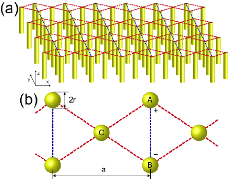
Here, we consider a 2D PC structure where infinitely long dielectric nanopillars are arranged periodically to form a specific lattice, as displayed in Fig. 1(a). Such a lattice structure is described by an array of quasi-1D tunable diamond (TD) lattices. Let us notice that the dielectric nanopillars in the array are infinitely long in the vertical direction, so that we may regard it as a 2D PC, assuming homogeneous electromagnetic fields along the direction.
The unit cell of the 2D PC contains three nanopillars, which can be split into two sublattices: majority (A and B) and minority (C), as depicted in Fig. 1(b). Note that coupling between A (or B) and C differs from that between A and B. All dielectric nanopillars are identical with radius , and the period of the TD lattice is . In our 2D PC, this quasi-1D TD lattice is repeated with the period , forming a square unit cell with three sublattices.
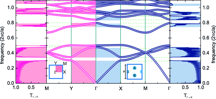
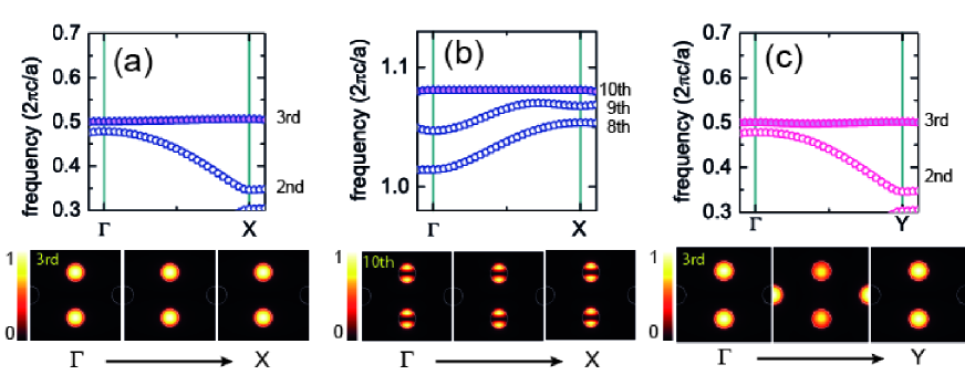
In order to determine the presence of the FBs, we investigate the optical properties of the 2D PC by numerical simulations in both frequency and time domains, using freely available MPB and MEEP software packages, respectively44, 45. Figure 2(a) shows the photonic band structure for TE polarization ( but ) of the PC calculated in the 2D Brillouin zone. The PC exhibits a wide band gap from to 0.67, a narrow band gap from to 0.84, and so on. Here, we focus on the photonic bands along the line in momentum space, which corresponds to the one-dimensional nature of the quasi-1D TD lattice laid along the direction in real space. Indeed, one can see that there are two FBs at specific frequencies and 1.08, as shown in Fig. 3(a) and (b). These FBs, which correspond to the third and tenth bands, are found to be flat only along the line. Indeed, we achieve strongly localized electromagnetic waves in A and B, resulting in zero field intensity in C. (see lower pannels in Fig. 3(a) and (b))
Since the FB reflects the existence of CLSs, propagation of light is expected to be prohibited at the flat-band frequencies in PCs. In order to examine the role of FBs for light propagation through the PC, we investigate the optical responses of the PC to a plane wave with TE polarization. We now consider a finite length of the PC in the direction with a periodic boundary condition in the direction. Twenty-one unit cells along the direction are taken into account in the FDTD simulation, a number believed to be large enough to reflect the photonic band structure that we found in the infinite PC. We put a plane wave source sufficiently far away from one facet of the finite PC, and calculate the energy flux of the transmitted wave throughout the PC to yield optical transmittance as a ratio of energy fluxes between incident and transmitted waves. The rightmost and leftmost pannels of Fig. 2 show the transmittance spectra and as functions of the incident plane wave frequency in the and directions, respectively. exhibit photonic band gaps in the specific frequency ranges where transmittance drops to zero. Overall, the photonic band gaps are well reflected in the transmittance spectra. However, we observe that certain photonic bands along the line seem to have no contribution to . As displayed by the shaded regions in Fig. 2, the third, seventh, eighth, and tenth bands seem to not be involved in . The reason for these inactive photonic bands will be discussed in the next subsection.
On the other hand, let us consider optical transmittance through the 2D PC with a plane wave source propagating along the direction. Because the unit cell considered in this study contains three sublattices that are anisotropic (i.e., the unit cell has no symmetry with respect to 90∘ rotation), the PC exhibits an anisotropic photonic band structure (Fig. 2) where the symmetric point replaces in Fig. 2(a). Overall, is similar to , but a distinguishing feature is that the third band along now contributes to optical transmittance. As highlighted in Fig. 3(c), the third band still seems to be flat over . However, by investigating the related field intensities along the line, it is revealed to be a dispersive band, as displayed in the lower panel of Fig. 3(c), so that the electromagnetic wave can be transferred from A and B to C, and vice versa.
1.2 Field distributions and compact localized states
The optical property analysis results of the 2D PC in this study introduce two important questions: i) how the flat bands differ from the dispersive bands, and ii) why certain photonic bands, including the FBs, have no contribution to the optical transmittance. To answer these questions, we analyze field distribution in the unit cell of the PC for the resulting photonic bands.
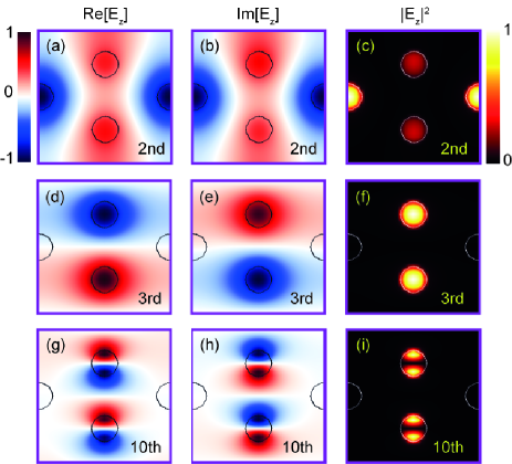
We first compare the electric field distributions of the flat and dispersive bands. As shown in Fig. 4, both dispersive and FBs exhibit a distinguishing distributions of field intensity . The second band, which is found to be dispersive in Fig. 2(a), indeed has a state that spreads over the unit cell, whereas the third band supports CLSs as is strongly localized in A and B nanopillars only. Such a localization of the electric field results from destructive interference in the C nanopillar as the electric fields in A and B have the opposite sign. On the other hand, the dispersive band comprises the same sign electric fields in A and B, causing constructive interference in C. It is worth mentioning that the dispersive and FBs can be characterized by even and odd parities in the direction of the unit cell, respectively.
As aforementioned, two FBs were found in the given frequency range to , corresponding to the third and tenth bands. Like the third band, the tenth band also exhibits a strong localization of electric field intensity. By comparing the electric fields in Fig. 4(d) and (e), and (g) and (h), one can easily see that the tenth FB is attributed to odd parity with respect to the direction like the third band. Further, the tenth band occurs as a consequence of destructive interference between excited modes in A and B nanopillars, contrary the to fundamental modes for the third band.
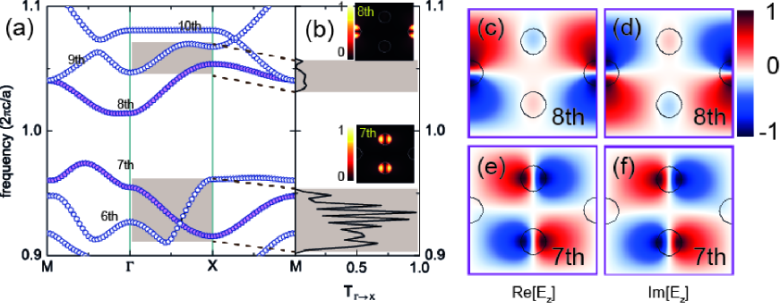
At this time, it should be noted that our electromagnetic wave source is provided as a plane wave propagating along the direction, in other words, the plane wave source is characterized as even parity with respect to the direction. This even-parity plane wave source does not excite the FBs, so that the FBs (the third and tenth bands) are not reflected in the transmittance spectra, as shown in Fig. 2. This is because the FBs are dark modes with respect to the plane-wave source. Similarly, the seventh and eighth bands are also dark, as highlighted by color-filed symbols in Fig. 5(a). By investigating their electric field patterns, we reveal that both the seventh and eighth bands indeed have odd parity with respect to the direction (see Fig. 5). Here, let us notice that there are slight mismatches between the shaded regions in Fig. 5(a) and (b), which are because of finite-resolution errors.
1.3 Self-collimation of light propagation
Due to the anisotropy of the 2D PC, the transmittance spectra with an incident wave along the direction are different from those for the direction (see Fig. 2). In particular, it is worthwhile to note that is nonzero at frequencies and 1.08, corresponding to the FBs along the line. In other words, we expect anisotropic light propagation throughout the 2D PC at the flat-band frequencies.
Now, we consider point sources inside the 2D PC instead of a plane wave source outside the PC. The point source radiates isotropic light with a frequency precisely set at , which is the frequency of the fundamental FB (third band). In order to examine the effects of parity, we place two monochromatic point sources at the centers of A and B nanopillars by changing their phase difference. Here, we stimulate a finite size (2121 unit cells), and for simplicity, observe light propagation before the radiated waves are reflected from the boundaries of the PC.
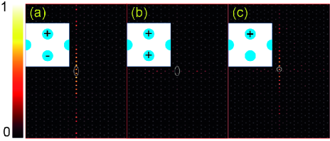
Figure 6 shows the field intensities with in-phase and out-of-phase point sources on A and B after some time steps in the FDTD simulations. As expected, for the out-of-phase point sources, the odd-parity waves in A and B nanopillars correspond to the FB shown in Fig. 3(a), resulting in prohibited light propagation in the direction. Therefore, we observe an interesting optical phenomenon where the radiated light from the point sources is strongly collimated into the direction, as exhibited in Fig. 6(a). Such a phenomenon is called “self-collimation”—light propagation is allowed in one only direction because of vanishing group velocity in the perpendicular directions.46, 47, 48 On the other hand, for the in-phase point sources, there is no photonic mode correlated with the even-parity waves in A and B, resulting in marginal effects in terms of light propagation (see very low field intensity in Fig. 6(b)).
As the existence of FBs has been believed to be a consequence of destructive interference, not only opposite phases but also equal amplitudes of the electromagnetic waves are therefore required. Despite this, the self-collimation effects still remain observable even with a single point source, as displayed in Fig. 6(c). Such a robustness of the FB-induced collimation effect is understood as follows. The out-of-phase and in-phase excitations in use for Figs. 6(a) and (b) are represented as vector and ; the former corresponds to the FB mode whereas the latter does not. On the other hand, the single-source excitation in Fig. 6(c) is expressed as a vector composed of the linear combination of and , i.e., . One can easily see that is always dominant, since barely affects light propagation in the PC. Consequently, the self-collimation effect in the FB PC is expected to be observable with arbitrary excitations in A and B.
2 Conclusions
We have investigated the photonic band structure and optical properties of a two-dimensional photonic crystals, which is constructed by a periodic array of quasi-1D tunable diamond lattices. It has been shown that the 2D PC exhibits flat bands only along the line in the Brillouin zone, reflecting the existence of compact localized states as a consequence of destructive interference between the odd-parity waves in the A and B nanopillars. Thus, we can conclude that the FBs of the TD lattice remain even if the TD lattices are not isolated. We have also found that FBs occur not only for the fundamental modes but also for excited modes in the nanopillars. Further, we have learned that the FBs are not involved in optical transmittance through the PC because of their nondispersive nature. Moreover, by changing the direction of the incident plane wave, the anisotropy of the photonic bands and transmittance spectra were investigated. This anisotropic property of the 2D PC leads to an intriguing optical phenomenon—the self-collimation of light propagation, resulting from the existence of the nondispersive FB .
Flat band-induced strong localization acquired in disorder-free PCs can be widely employed to send photons over long distances with optical fiber communication technology. Also, our finding of a self-collimation effect at FB frequency may be practically applicable to photonic and metamaterial research.
This work was supported by Project IBS-R024-D1, the National Research Foundation of Korea (NRF) grant funded by the Korea government (MSIT) (No. 2017076824), and research funds from Chosun University 2017.
References
- Mekis et al. 1996 Mekis, A.; Chen, J. C.; Kurl, I.; Fan, S.; Vileneuve, P. R.; Joannopoulos, J. D. High transmission through sharp bends in photonic crystal waveguides. Phys. Rev. Lett. 1996, 77, 3787–3790
- Foresi et al. 1997 Foresi, J. S.; Villeneuve, P. R.; Ferrera, J.; Thoen, E. R.; Steinmeyer, G.; Fan, S.; Joannopoulos, J. D.; Kimerling, L. C.; Smith, H. I.; Ippen, E. P. Photonic-bandgap microcavities in optical waveguides. Nature 1997, 390, 143–145
- Broeng et al. 1999 Broeng, J.; Mogilevstev, D.; Barkou, S. E.; Bjarklev, A. Photonic crystal fibers: a new class of optical waveguides. Opt. Fiber Technol. 1999, 5, 305–330
- Hood et al. 2016 Hood, J. D.; Goba, A.; Asenjo-Garcia, A.; Lu, M.; Yu, S.-P.; Chang, D. E.; Kimble, H. J. Atom-atom interactions around the band gap of a photonic crystal waveguide. Proc. Nat. Am. Soc. 2016, 113, 10507–10515
- Faggiani et al. 2016 Faggiani, R.; Baron, A.; Zang, X.; Lalouat, L.; Schulz, S. A.; O’Regan, B.; Vynck, K.; Cluzel, B.; de Fornel, F.; Krauss, T. F.; Lalanne, P. Lower bound for the spatial extent of localized modes in photonic-crystal waveguides with small random imperfections. Sci. Rep. 2016, 6, 27037
- Jandieri et al. 2017 Jandieri, V.; Khomeriki, R.; Erni, D.; Chew, W. C. Realization of all-optical digital amplification in coupled nonlinear photonic crystal waveguides. Prog. Electromagn, Res. 2017, 158, 63–72
- Zeng et al. 2006 Zeng, L.; Yi, Y.; Hong, C.; Liu, J.; Feng, N.; Duan, X.; Kimerling, L. C.; Alamariu, B. A. Efficiency enhancement in Si solar cells by textured photonic crystal back reflector. Appl. Phys. Lett. 2006, 89, 111111
- Bermel et al. 2007 Bermel, P.; Luo, C.; Zeng, L.; Kimering, L. C.; Joannopoulos, J. D. Improving thin-film crystalline silicon solar cell efficiencies with photonic crystals. Opt. Exp. 2007, 15, 16986–17000
- Florescu et al. 2008 Florescu, M.; Lee, H.; Puscasu, I.; Pralle, M.; Florescu, L.; Ting, D. Z.; Dowling, J. P. Improving solar cell efficienty using photonic band-gap materials. Sol. Energy Mater. Sol. Cells 2008, 91, 1599–1610
- Mutitu et al. 2008 Mutitu, J. G.; Shi, S.; Chen, C.; Creazzo, T.; Barnett, A.; Honsberg, H.; Prather, D. W. Thin film silicon solar cell design bansed on photonic crystal and diffractive grating structures. Opt. Exp. 2008, 16, 15238–15248
- Colodero et al. 2009 Colodero, S.; Mihi, A.; Häggman, L.; Ocaña, M.; Boschloo, G.; Hagfeldt, A.; Míguez, H. Poros one-dimensional photonic crystals improve the power-conversion efficiency of dey-sensitize solar cells. Adv. Mater. 2009, 21, 764–770
- Liu et al. 2016 Liu, L.; Barber, G. D.; Shuba, M. V.; Yuwen, Y.; Lakhtakia, A.; Mallouk, T. E.; Mayer, T. S. Planar light concentration in micro-Si solar cells enabled by a metallic grating-photonic crystal architecture. ACS Photon. 2016, 3, 604–610
- Painter et al. 1999 Painter, O.; Lee, R. K.; Scherer, A.; Yariv, A.; O’Brien, J. D.; Dapkus, P. D.; Kim, I. Two-Dimensional Photonic B and-Gap Defect Mode Laser. Science 1999, 284, 1819–1821
- Meier et al. 1999 Meier, M.; Mekis, A.; Dodabalapur, A.; Timko, A.; Slusher, R. E.; Joannopoulos, J. D.; Nalamasu, O. Laser action from two-dimensional distributed feedback in photonic crystals. Appl. Phys. Lett. 1999, 74, 7–9
- Park et al. 2004 Park, H. G.; Kim, S. H.; Kwon, S. H.; Ju, Y. G.; Yang, J. K.; Baek, J. H.; Kim, S. B.; Lee, Y. H. Electrically Driven Single-Cell Photonic Crystal Laser. Science 2004, 305, 1444–1447
- Hirose et al. 2014 Hirose, K.; Liang, Y.; Kurosaka, Y.; Watanabe, A.; Sugiyama, T.; Noda, S. Watt-class, High-power, high-beam-quality photonic-crystal laser. Nat. Photon. 2014, 8, 406–411
- Wu et al. 2015 Wu, S.; Buckley, S.; Shcaibley, J. R.; Feng, L.; Yan, J.; Mandrus, D. G.; Hatami, F.; Yao, W.; Vǔković, J.; Majumdar, A.; Xu, X. Monolayer semiconductor nanocavity lasers with ultralow thersholds. Nature 2015, 520, 69–72
- Chen et al. 2016 Chen, S.; Rho, K.; Lee, J.; Chong, W. K.; Lu, Y.; Mathews, N.; Sum, T. C.; Nurmikko, A. A photonic crystal laser from soliton based organo-lead iodide perovskite thin films. ACS Nano 2016, 10, 3959–3967
- Yokoo et al. 2017 Yokoo, A.; Takiguchi, M.; Boriwosuto, M. D.; Tateno, K.; Zhang, G.; Kuramochi, E.; Shinya, A.; Taniyama, H. Subwavelength nanowire lasers on a silicon photonic crystals operating at telecom wavelengths. ACS Photon. 2017, 4, 335–362
- Hwang et al. 2017 Hwang, M.-S.; Kim, H.-R.; Kim, K.-H.; Jeong, K.-Y.; Park, J.-S.; Choi, J.-H.; Kang, J.-H.; Lee, J. M.; Park, W. I.; J.-H., S.; Seo, M.-K.; Park, H.-G. Switching of photonic crystal lasers by graphene. Nano Lett. 2017, 17, 1892–1998
- Villeneuve et al. 1996 Villeneuve, P. R.; Fan, S.; Joannopoulos, J. D. Microcavities in photonic crystals: mode symmetry, tunability, and coupling efficiency. Phys. Rev. B 1996, 54, 7837–7842
- Bayindir et al. 2000 Bayindir, M.; Temelkuran, B.; Ozbay, E. Tight-binginf description of the coupled defect modes in three-dimensional photonic crystals. Phys. Rev. Lett. 2000, 84, 2140–2143
- Regensburger et al. 2013 Regensburger, A.; Miri, M.-A.; Bersch, C.; Näger, J.; Onishchukov, G.; Christodoulides, D. N.; Peschel, U. Observation of defect states in -symmetric optical lattices. Phys. Rev. Lett. 2013, 110, 223902
- Gao et al. 2016 Gao, Z.; Gao, F.; Zhang, B. Guiding, bending, and splitting of coupled defect surface modes in a surface-wave photonic crystals. Appl. Phys. Lett. 2016, 108, 041105
- Schwartz et al. 2007 Schwartz, T.; Bartal, G.; Fishman, S.; Segev, M. Transport and Anderson localization in disordered two-dimensional photonic lattices. Nature 2007, 446, 52–55
- Topolancik et al. 2007 Topolancik, J.; Ilic, B.; Vollmer, F. Experimental observation of strong photon localization in disordered photonic crystal waveguides. Phys. Rev. Lett. 2007, 99, 253901
- Liu et al. 2014 Liu, J.; Garcia, P. D.; Gregersen, S. E. N.; Suhr, T.; Schubert, M.; Mørk, J.; Stobbe, S.; Lodahl, P. Randon nonlasing in the Anderson localized regime. Nat. Nanotechnol. 2014, 9, 285–289
- Roque et al. 2017 Roque, T. F.; Peano, V.; Yevtushenko, O. M.; Marquardt, F. Anderson localization of composite excitations in disordered optomechanical arrays. New J. Phys. 2017, 19, 013006
- Vasco and Hughes 2017 Vasco, J. P.; Hughes, S. Anderson localization in disordered LN photonic crystal slab cavities. arXiv:1708.07891 2017,
- Levi et al. 2011 Levi, L.; Rechtsman, M.; Freedman, B.; Schwartz, T.; Malena, O.; Segev, M. Disorder-enhanced transport in photonic quasicrystals. Science 2011, 332, 1541–1544
- Hsieh et al. 2015 Hsieh, P.; Chung, C.; McMillan, J. F.; Tsai, M.; Panoiu, N. C.; Wong, C. W. Photon transport enhanced by transverse Anderson localization in disordered superlattices. Nat. Phys. 2015, 11, 268–274
- Flach et al. 2014 Flach, S.; Leykam, D.; Bodyfelt, J. D.; Matthies, P.; Desyatnikov, A. S. Detangling flat bands into Fano lattices. Eur. Phys. Lett. 2014, 105, 30001
- Milina 2015 Milina, M. I. Flat bands and symmetry in quasi-one-dimensional lattices. Phys. Rev. A 2015, 92, 063813
- Khomeriki and Flach 2016 Khomeriki, R.; Flach, S. Landau-Zehner Bloch oscillations with perturbed flat bands. Phys. Rev. Lett. 2016, 116, 245301
- Leykam et al. 2017 Leykam, D.; Bodyfelt, J. D.; Desyatnikov, A. S.; Flach, S. Localization of weakly disordered flat band states. Eur. Phys. J. B 2017, 90, 1
- Maimaiti et al. 2017 Maimaiti, W.; Andreanov, A.; Park, H. C.; Gendelman, O.; Flach, S. Compact localized states and flat-band generators in one dimensions. Phys. Rev. B 2017, 95, 115135
- Baboux et al. 2016 Baboux, F.; Ge, L.; Jacqmin, T.; Biondi, M.; Galopin, E.; Lemaître, A.; Le Gratiet, L.; Sagnes, I.; Schmidt, S.; Türeci, H. E.; Amo, A.; Bloch, J. Bosonic condensation and disorder-induced localization in a flat band. Phys. Rev. Lett. 2016, 116, 066402
- Travkin et al. 2017 Travkin, E.; Diebel, F.; Denz, C. Compact flat band states in optically induced flatland photonic lattices. Appl. Phys. Lett. 2017, 111, 011104
- Rojas-Rojas et al. 2017 Rojas-Rojas, S.; Morales-Inostroza, L.; Vicencio, R. A.; Delgado, A. Quantum localized states in photonic flat-band lattices. Phys. Rev. A 2017, 96, 043803
- Perchikov and Gendelman 2017 Perchikov, N.; Gendelman, O. V. Flat bands and compactons in mechanical lattices. Phys. Rev. E 2017, 96, 052208
- Mukherjee et al. 2015 Mukherjee, S.; Spracklen, A.; Choudhury, D.; Goldman, N.; Öhberg, P.; Andersson, E.; Thomson, R. R. Observation of a localized flat-band state in a photonic Lieb lattice. Phys. Rev. Lett. 2015, 114, 245504
- Xia et al. 2016 Xia, S.; Hu, Y.; Song, D.; Zong, Y.; Tang, L.; Chen, Z. Demonstration of flat-band image transmission in optically induced Lieb photonic lattices. Opt. Lett. 2016, 41, 1435–1438
- Weimann et al. 2016 Weimann, S.; Morales-Inostroza, L.; Real, B.; Cantillano, C.; Szameit, A.; Vicencio, R. A. Transport in sawtooth photonic lattices. Opt. Lett. 2016, 41, 2414–2417
- Johnson and Joannopoulos 2001 Johnson, S. G.; Joannopoulos, J. D. Block-iterative frequency-domain methods for Maxwell’s equations in a planewave basis. Opt. Exp. 2001, 8, 173–190
- Oskooi et al. 2010 Oskooi, A.; Roundy, D.; Ibanescu, M.; Bermel, P.; Joannopoulos, J.; Johnson, S. MEEP: A flexible free-software package for electromagnetic simulations by the FDTD method. Comput. Phys. Commun. 2010, 181, 687–702
- Kosaka et al. 1999 Kosaka, H.; Kawashima, T.; Tomita, A.; Notomi, M.; Tamamura, T.; Sato, T.; Kawakami, S. Self-collimating phenomena in photonic crystals. Appl. Phys. Lett. 1999, 74, 1212
- Witznens et al. 2002 Witznens, J.; Loncar, M.; Scherer, A. Self-collimation in planar photonic crystals. IEEE J. Sel. Top. Quantum Electron. 2002, 8, 1246–1257
- Yu and Fan 2003 Yu, X.; Fan, S. Bends and splitters for self-collimated beams in photonic crystals. App. Phys. Lett. 2003, 83, 3251