Present Address]: Max Planck Institute for Chemical Physics of Solids, Dresden, Germany Present Address ]: Institute for Solid State Research, IFW Dresden, Germany.
Microstructural control of the transport properties of -FeSe films grown by sputtering
Abstract
We have investigated the correlation between structural and transport properties in sputtered -FeSe films grown onto SrTiO3 (100). The growth parameters, such as substrate temperature and thickness, have been varied in order to explore different regimes. In the limit of textured thick films, we found promising features like an enhanced K, a relatively high and a low anisotropy. By performing magnetoresistance and Hall coefficient measurements, we investigate the influence of the disorder associated with the textured morphology on some features attributed to subtle details of the multi-band electronic structure of -FeSe. Regarding the superconductor-insulator transition (SIT) induced by reducing the thickness, we found a non-trivial evolution of the structural properties and morphology associated with a strained initial growth and the coalescence of grains. Finally, we discuss the origin of the insulating behavior in high-quality stressed epitaxial thin films. We found that a lattice distortion, described by the Poisson’s coefficient associated with the lattice parameters a and c, may play a key role.
I Introduction
Among the iron-based superconductors, iron selenide stands out as a rich system for studying new emergent phenomena. Particular interest in this material has been triggered by the strong enhancement of the superconducting critical temperature with pressure (hydrostatic Sun et al. (2016); Medvedev et al. (2009) or residual stress Nabeshima et al. (2013); Imai et al. (2016)) and the reports of the opening of a superconducting gap above K in extremely thin FeSe films grown by MBE Liu et al. (2012); Wang et al. (2012). In the last case, interface charging and/or electron-phonon coupling are proposed as the mechanism responsible for raising the critical temperature. From the fundamental point of view, interesting behavior has been reported in this material such as a multi-band electronic structure Lei et al. (2012); Watson et al. (2015), tetragonal to orthorhombic McQueen et al. (2009) and nematic phase transitions at K Böhmer et al. (2013, 2015).
It is also a promising candidate for applications given its high-field performance and as a candidate for the construction of cryogenic sensors. The potential use of Fe-based superconductors in the electronics sector has been discussed by Haindl et al Haindl et al. (2014). A particular perspective niche is the use of FeSe in the construction of Microwave Kinetic Inductance Detectors (MKID’s) Mazin (2009). The relatively high critical temperature of K would allow its use at temperatures in the range of 4He instead of miliKelvins, as occurs with the currently used materials. However, the integration in these devices requires the growth of high-quality thin films. Given this, it is important to understand the growth mechanism and how it affects the physical properties and morphology of the resulting material.
Despite the structural simplicity of this compound, high-quality bulk single crystals were obtained only years after its discovery Hsu et al. (2008); Chareev et al. (2013). The main feature of the temperature dependence of the resistivity is a superconducting transition at K followed by a semimetallic state at higher temperatures. Motivated for the potential technical applications Haindl et al. (2014), the challenge of growing thin films has been also faced up. Thin films of FeSe have been successfully synthesized by different growth methods such as pulsed laser deposition (PLD) Nabeshima et al. (2013); Imai et al. (2016); Nie et al. (2009); Chen et al. (2010), molecular beam epitaxy (MBE) Sun et al. (2016); Liu et al. (2012); Tan et al. (2013); Song et al. (2011) and in a lesser extent by sputtering Schneider et al. (2012, 2013); Speller et al. (2011); Venzmer, Kronenberg, and Jourdan (2016). Nevertheless, there are discrepancies between different authors with the transport properties of epitaxial films in the limit of small thicknesses, irrespective of the growth method. There are reports of both superconducting and semiconducting/insulating behavior. Since controlling the stoichiometry and/or the crystalline structure is still a challenging issue, a remaining question is whether minor structural or compositional changes are relevant. In the case of films grown by sputtering, this implies a superconductor-insulator transition (SIT) as a function of thickness Schneider et al. (2012); Wang et al. (2015). This kind of behavior has been discussed within a disordered granular superconductor scenario Schneider et al. (2012) where the disorder associated with smaller thickness induces a superconductor-insulator transition. In this context, fundamental questions concerning the mechanism governing the transition are still open.
In this work, we report on the fabrication of thin films of -FeSe by dc magnetron sputtering from stoichiometric targets, with the aim to study the influence on the transport properties of the structural characteristics in the atomic and mesoscopic scales. The phase purity and crystal structure of the films were characterized by X-ray diffraction measurement (XRD). The surface morphology was studied using a Scanning Electron Microscope (SEM) and an Atomic Force Microscope (AFM). The local chemical composition was measured by Energy-Dispersive X-ray Spectroscopy (EDX) and Rutherford Backscattering Spectrometry (RBS). The magnetization was measured in a commercial SQUID magnetometer. We carried out electrical transport measurements with magnetic fields up to T.
II Experimental details
Fe1-xSe thin films have been deposited by dc magnetron sputtering. The polycrystalline target was fabricated from Fe (%) and Se (%) grits. Two consecutive cycles of mixing, heating up to C for hours in an evacuated quartz tube, and milling were performed to favor the solid state reaction of the powder. Low heating rates were used while the temperature was close to the melting point of Se. In a final process, the powder was pressed and sintered at C for 4 days. X-ray diffraction and Rietveld refinement were performed at each stage to characterize the powder. The final target material was -FeSe with approximately % -Fe7Se8. A very small amount, <5 ‰, of FeO was also observed.
Films were grown onto SrTiO3 (100), labelled from now on as STO. The substrates were attached to a resistive heater with Ag paste, which allowed for heating up to a nominal temperature of 680∘C Pardo, Burmeister, and Guimpel (1996). The substrate temperature, , was measured and controlled with a thermocouple in direct thermal contact with the substrates. The base pressure of the sputtering system was Torr. The growth parameters that were kept constant for all films are sputtering gas, 99.999% pure Ar, and pressure, mTorr, target power, W for a " diameter target, and target to substrate distance, at cm. In this conditions, the growth rate is approximately nm/min. These parameters were found to be optimal in previous, unreported tests.
The chemical composition of the films has been routinely measured by EDX and for some samples also measured by Rutherford Backscattering Spectrometry (RBS). Under the conditions described above, all the samples have a composition close to the expected values, i.e. Fe:Se1:1, within the error in EDX analysis. The homogeneity of the films was also investigated by performing several spot and area analysis over different regions. No spatial variations were found.
The thickness of the films was measured by contact profilometry in well-defined steps. These steps were generated by first masking part of the substrates with silver epoxy, growing the films, and finally removing the epoxy. For thin films, the thickness was also determined through low angle X-Ray reflectivity, XRR, measuring the periodicity of the Kiessig fringes Kiessig (1931). When the later were observed, both methods of thickness determination coincided within 10 %.
The diffraction patterns were measured at room temperature with two different diffractometers: a PANalytical Empyrean diffractometer or a Phillips PW 3710 in Bragg-Brentano geometry with Cu Kα radiation. In the former case, the samples were mounted in a 4-circle Eulerian cradle, which allowed for precise alignment. Due to physical limitations of the Eulerian cradle, a monochromator could not be used. Instead, a Ni filter was used to diminish the Cu Kβ radiation. For the extremely intense substrate diffraction, the Kβ peak and the Ni absorption edge are visible in the data, the later as a step-like discontinuity in the background intensity between the Kα and Kβ peaks.
Electrical transport properties were measured in a standard 4 probe geometry, defined by UV photo-lithography and ion milling. For the Hall effect measurements, two probes at both sides of the current carrying line were added. The measurements were performed in an Oxford cryostat equipped with an T superconducting coil and sample rotation capability, in the K to K range.
III Results and discussion
Since previous systematic studies showed a complex influence of growth conditions on the structural and physical properties of the films, we choose the growth parameters, such as substrate temperature and thickness, in order to explore different regimes. First, we focus on textured thick films with optimal superconducting properties. Second, regarding the superconductor-insulator transition (SIT) induced by reducing the thickness, we performed a comprehensive study of the evolution of the structural properties and morphology. Finally, we discuss the origin of the insulating behavior on epitaxial stressed films.
III.1 Superconducting thick films
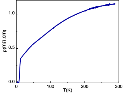
Since the properties which are sought to optimize for integrating FeSe films in devices are the superconducting ones, first we will focus on what we found to be the “best" superconducting properties. The optimal parameters for growing a superconducting film on STO, i.e. those which produce the highest, , and sharpest, K, superconducting transition are C and thickness nm. These values of superconducting onset are slightly higher than the previously reported for macroscopic high-quality samples, K Chareev et al. (2013), and sputtered films, K Schneider et al. (2012, 2013); Venzmer, Kronenberg, and Jourdan (2016). As a representative example of the temperature dependence of the electrical resistivity, Figure 1 shows in the K range of one of these films. Besides the superconducting transition at low temperature, a semimetallic like behavior is observed in the normal state with a negative curvature up to room temperature.
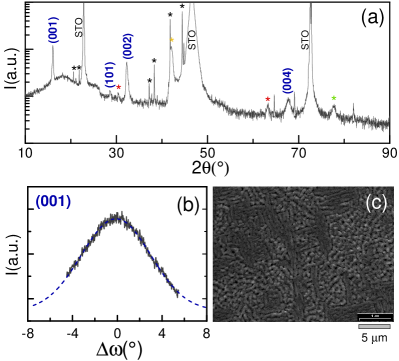
Regarding the crystalline structure, Figure 2(a) shows the X-ray diffraction data for the same film. The most intense peaks can be indexed as the (00l) -FeSe family. The rest of the peaks can be identified as substrate related or low intensity (101) -FeSe and (001) -Fe7Se8. The (001) peak rocking curve has a full width at half maximum (FWHM) of approximately 5, indicating textured growth (Figure 2(b)). These results indicate preferred c-axis growth, with coexisting small inclusions of (101) -FeSe and (001) -Fe7Se8. The SEM topography, Figure 2(c), shows a tweed grain pattern with a characteristic length around m. We previously reported a similar increase of for bulk crystals with a nanoscale intergrowth of -FeSe and -Fe7Se8 Amigó et al. (2017a). Since there are also inclusions in the sputtered films, the enhancement could be related to the presence of this type of defect. However, another possibility which cannot be neglected is the existence of local tensile stress due to grain matching.
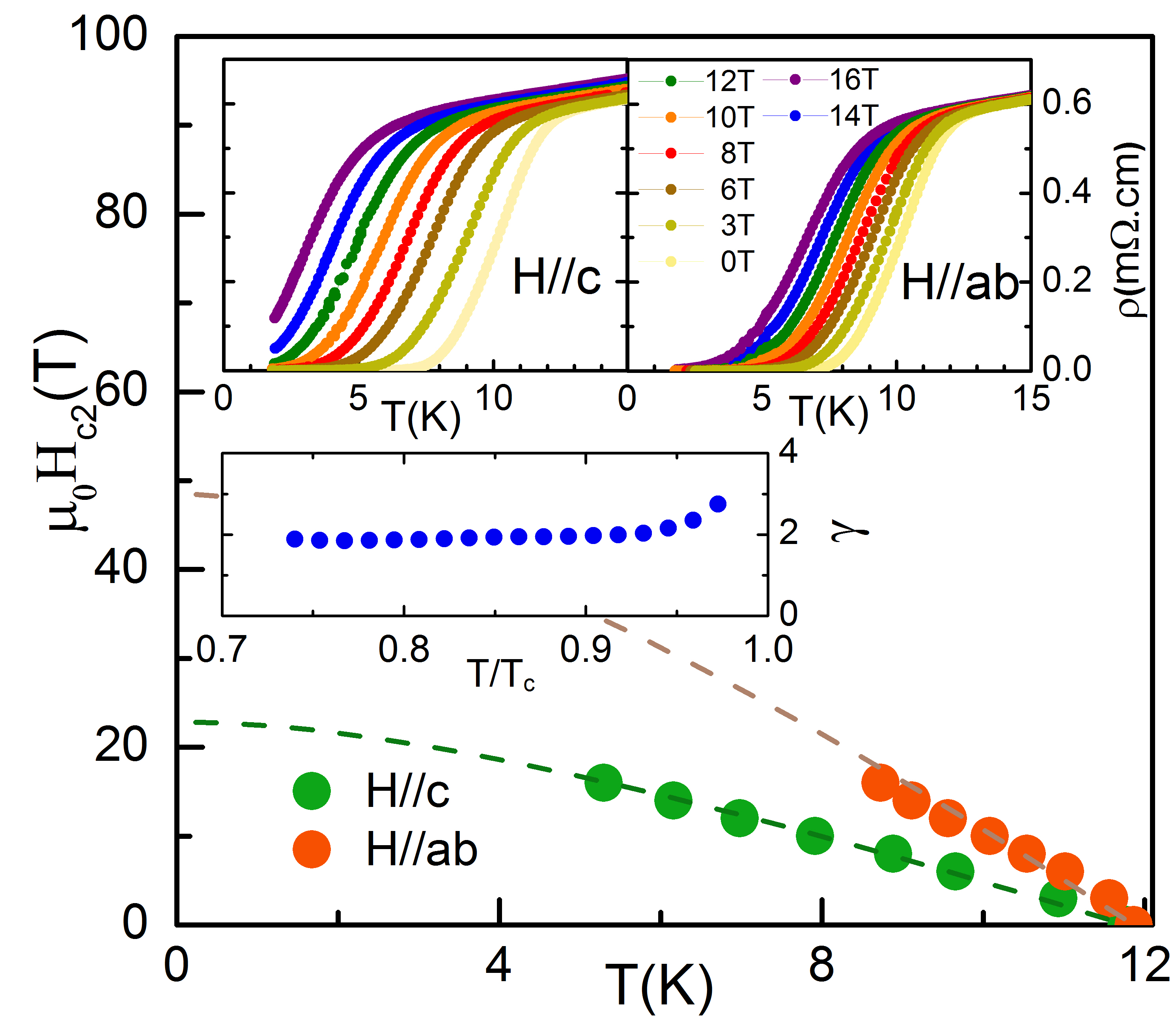
From the point of view of high-field applications, properties as the critical field and its anisotropy are relevant. The top insets in Figure 3 show the evolution of the superconducting transition with applied field parallel and perpendicular to the substrate surface, which corresponds mainly to magnetic field along the ab plane and along c axis, respectively. From these curves the transition temperatures are determined and so the perpendicular and parallel critical fields, and , which are shown in the main figure. The dotted lines correspond to the dependence predicted by the Werthamer-Helfand-Hohenberg (WHH) model. Determining the slope of in the vicinity of and using the WHH model Werthamer, Helfand, and Hohenberg (1966), the values of are estimated as T and T, in accordance with the previously reported values Nabeshima et al. (2013); Terashima et al. (2014). From the Ginzburg Landau relations for D superconductor in the clean limit Haindl et al. (2014), the estimated values for coherence lengths at zero temperature are nm and nm. Since these values are considerably smaller than the film thickness and the grain size, our use of the 3D Ginzburg Landau equations is justified. Consequently, the difference between and can be interpreted as due to the intrinsic -FeSe anisotropy. The anisotropy, defined as , takes a maximum value of at K and decreases for lower temperatures (see bottom inset). These values are probably underestimated due to the presence of misaligned grains, but they are not far from the reported values. Indeed, this anisotropy lies within the reported curves for pure -FeSe bulk crystals and for crystals with impurity phases Amigó et al. (2015).
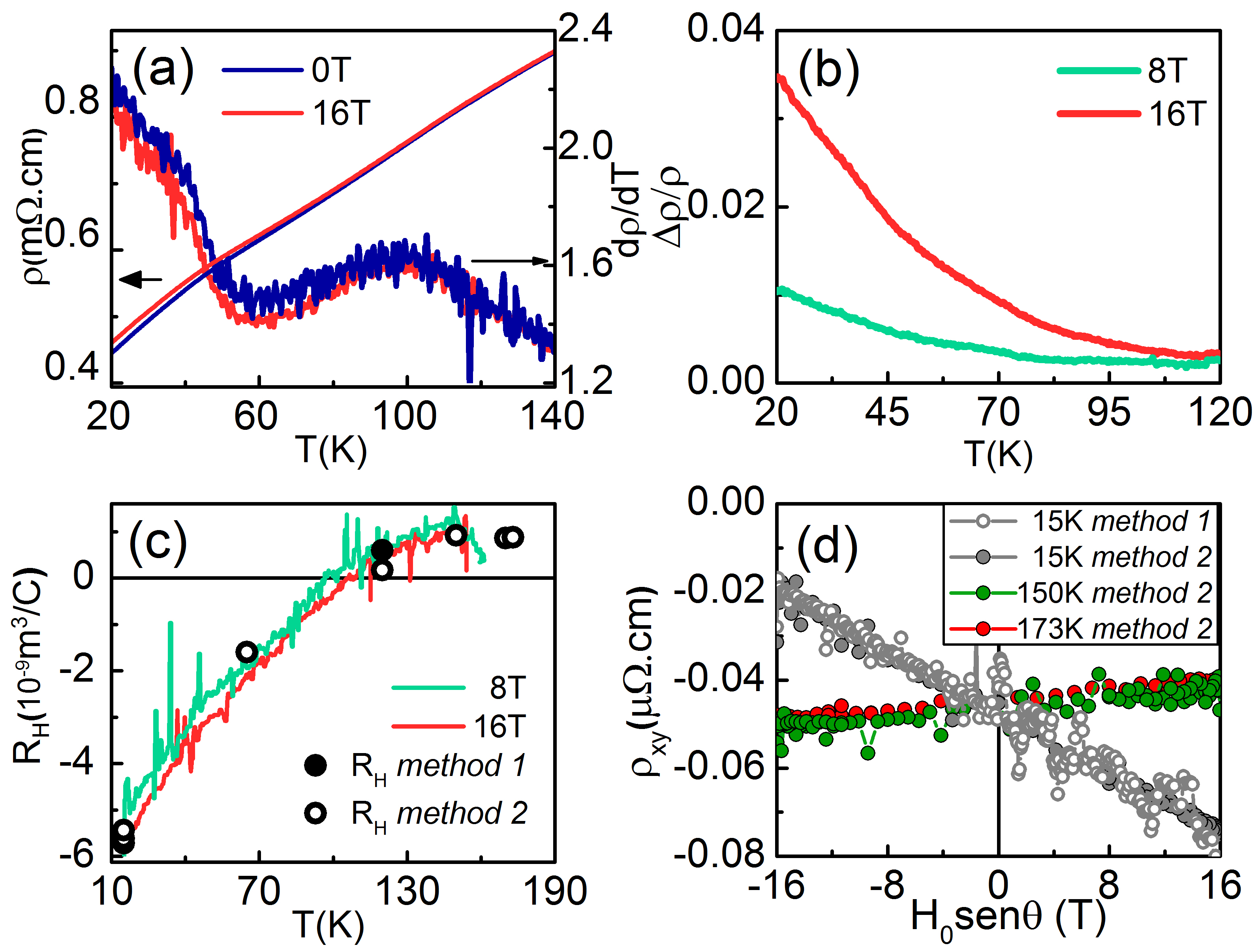
Coming back to the transport properties in the normal state, our sample mimics some features reported in the literature. The data in Figure 1 shows a smooth slope change that begins at K and extends to lower temperatures, instead of the usually abrupt slope change at K correlated to the structural transition for -FeSe McQueen et al. (2009). This feature is zoomed in the Figure 4 (a), together with . Data with an applied magnetic field of T perpendicular to the substrate surface is also included. Figure 4 (b) shows the temperature dependence of the transversal magnetoresistance, , with and T. A positive magnetoresistance is observed below the structural transition, which increases as the temperature decreases. We emphasize that this was mainly reported for bulk high-quality single crystals Kasahara et al. (2014); Amigó et al. (2014), although it has also been reported for nm thick PLD grown films Feng et al. (2018).
More information on the electronic structure is obtained from Hall-effect measurements. The Hall coefficient , which has been measured with three different protocols (see caption of Fig. 4 (c)), takes small positive values above the structural transition, and shows a sign reversal to negative values for , with K. This change of sign is reminiscent of the one presented by single crystals close to this transition, which has been associated with the structural distortion and originating in the multiband character of -FeSe Watson et al. (2015); Kasahara et al. (2014). Nevertheless, there is a striking difference at low temperatures; below our films present a linear Hall resistivity up to T, in contrast to the nonlinear behavior observed in high-quality single crystals Watson et al. (2015). Figure 4 (d) shows the linear dependence of the Hall resistivity, , with the magnitude of the applied magnetic field at , and K. It is known that depends strongly on the nature of the FeSe samples. For instance, bulk single-crystal exhibit non-linear behavior reveling a multiband feature, while exfoliated single-crystalline flakes and thin films show linear behavior Lei et al. (2016); Feng et al. (2018). We emphasize that some features like the sign reversal of the Hall coefficient and a concomitant positive magnetoresistance are robust in our samples against the presence of impurity phases and the disorder associated with the grains texture. Overall, the differences found may shed light on what aspects of bulk single crystals are more sensitive to this kind of imperfections.
In summary, from the point of view of potential applications, the enhanced , the relatively high and the low anisotropy are promising features of the films grown by sputtering at C with a thickness around nm. We investigate the influence of the disorder associated with a textured morphology on some transport properties attributed to subtle details of the multi-band electronic structure of -FeSe. In the normal state, we find that some distinctive characteristics of the nematic phase like changes in the resistivity, a positive transverse magnetoresistance and a sign reversal of the Hall coefficient, are robust against the type and degree of disorder present in the films. Nevertheless, we do not observe other features like a non-linear Hall effect.
III.2 Superconductor-insulator transition (SIT): Evolution of the crystalline structure and surface morphology
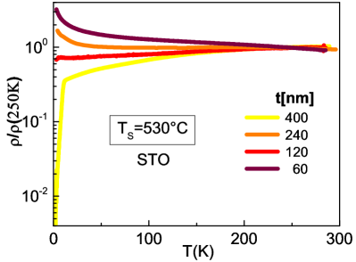
What is the effect of thickness on the physical properties of the films? Figure 5 shows the normalized electrical resistivity, , as a function of temperature, , for films of different thicknesses. Films were grown at the same C, under equivalent conditions on STO substrates. The thicknesses vary from to nm for deposition times between and min. A change from insulating to superconducting behavior is observed as the film thickness increases, indicating a superconductor-insulator transition (SIT) Schneider et al. (2012); Wang et al. (2015). It is worth to mention that this phenomenology seems to be a general feature of sputtering grown -FeSe films. In unreported tests, we observe this crossover in a wide range of (CC), independently of the substrate used (STO or MgO). We found that thin films (nm) present an insulating-like behavior, while the corresponding thicker films (nm) grown under equivalent condition show a metallic-like behavior and a superconductor transition at low temperatures.
In order to correlate this behaviour with the structural evolution of the films we also studied the crystalline structure and morphology as a function of thickness. Figure 6(a) shows a zoomed view of the XRD patterns in the range for the previously mentioned films. The diffraction pattern from an epitaxial thin film (nm) grown at C, which will be studied in detail in the next section, has been included for comparison. In all the cases, the (001) peak is observed. Only for the case of the epitaxial sample grown at C the lattice parameter is clearly contracted. On the thick film limit, nm, the peak has the same position as in the bulk material. The rest of the samples have almost the same lattice parameter with a small but noticeable tendency to be smaller. This implies that for higher thicknesses the tensile stress is relaxed.
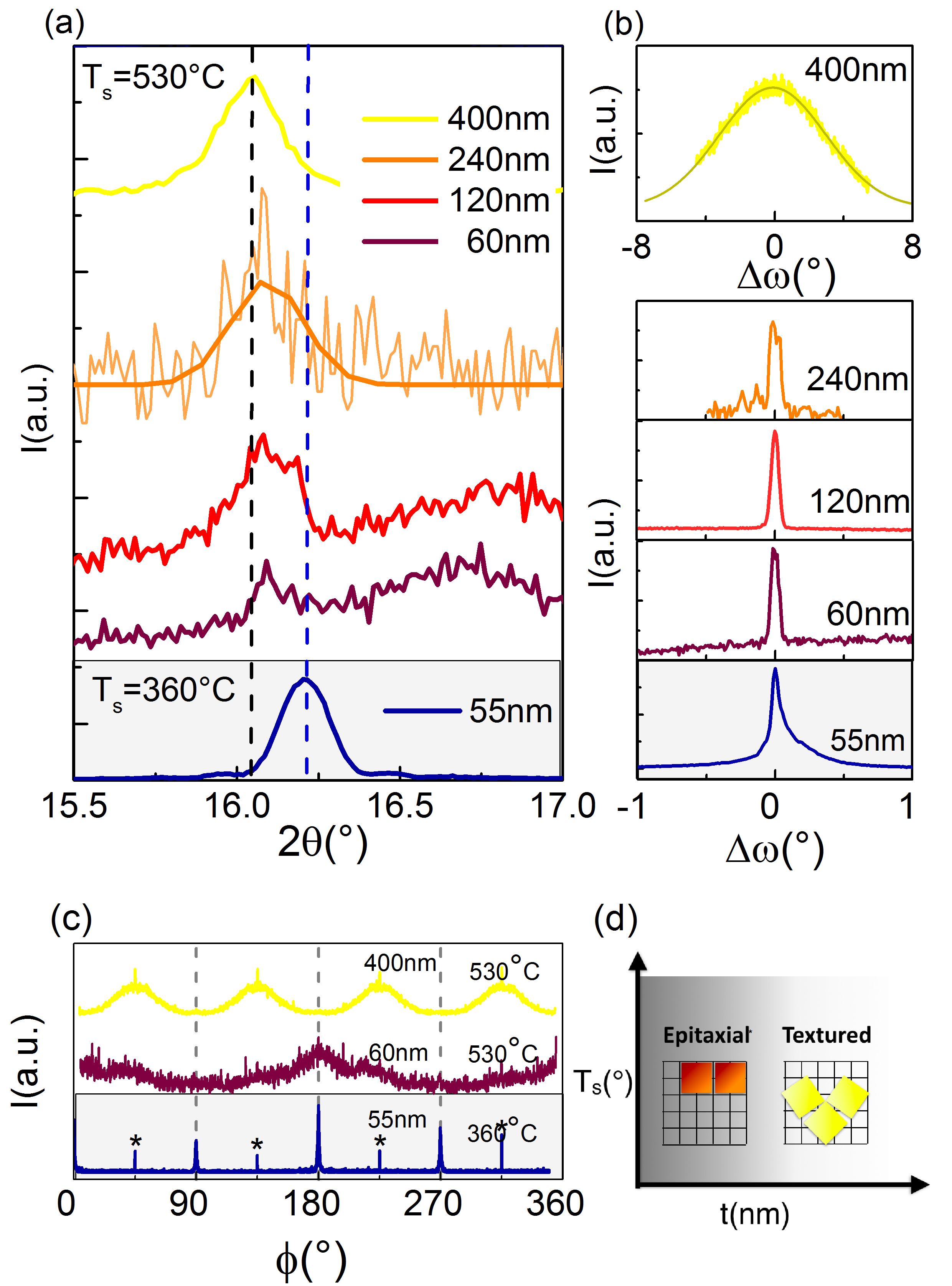
The full width at half maximum (FWHM) of the rocking curves (Figure 6(b)) indicates that the out-plane dispersion increase with the nominal thickness. There is also an evolution of the in-plane structure of the films. Figure 6(c) shows the azimuthal scans for the (101) -FeSe diffraction peak of the films. Vertical dashed lines show the position of the measured peaks in an equivalent azimuthal scan for the (101) diffraction of the STO substrate. The figure includes data for films grown at C with thicknesses nm and nm and a film grown at C with nm. It is clear that the thinner films present an in-plane alignment with the [100] -FeSe axis parallel to the [100] STO axis, which is optimal for C. However, the thicker films show a rotation in the structure with the [110] -FeSe axis parallel to the [100] STO axis. Different non cubic-on-cubic alignments have been reported previously Wang et al. (2009); Zhou et al. (2016). The Figure 6(d) is a schematic representation of the in-plane evolution as a function of thickness. Also, the width of the diffraction peaks is greatly increased after the rotation takes place. Our results are compatible with an initially stressed cube-on-cube growth which, after a critical thickness, relaxes through a 45 rotation around the vertical axis. This rotation is characterized by an increment of the in-plane and out-plane dispersion.
Regarding the morphology, in contrast to the tweed grain pattern of the superconducting sample, thinner films present a smoother surface. Notably, in the case of the sample grown at C the microstructural study of the surface morphology by SEM and AFM measurements revealed a continuous insulating matrix with small embedded particles (nm).
In conclusion, concomitant to the superconductor to insulator crossover there is a complex structural and morphological evolution. This phenomenology is in contrast to the strong -axis texture irrespective of the film thickness reported by Schneider et al Schneider et al. (2012). A plausible scenario is a Volmer-Weber island growth mode where the initial layers are characterized by a structural distortion. By increasing the nominal thickness, the tension relaxes and a regime of oriented grains emerge. This implies that percolation is a necessary condition for the macroscopic conduction mechanism to reflect the semimetallic and superconducting nature of -FeSe. A model to understand this phenomenology must be able to explain which is the origin of the insulating behavior in the epitaxial thin film grown at C, despite the lack of islands or cracks and the high-quality structural order.
III.3 Origin of the insulating behavior
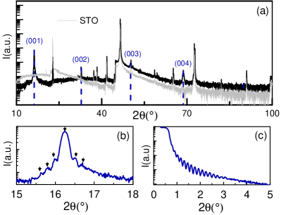
What could be the origin of the insulating behavior of stressed epitaxial films? To analyze this question, we focus on the epitaxial -FeSe (nm) films grown at C. The high-quality epitaxy of these films is evidenced by: i) the existence of only (00l) peaks in the diffraction curve (Fig. 7a); ii) the sharpness of the out-of-plane rocking curve (Fig. 6b) and iii) the highly oriented sharp peaks in the -scan (Fig. 6c). Also, a very homogeneous thickness is evidenced by the finite size effect peaks around the (001) peak (Fig. 7b) and the presence of Kiessig fringes in the low angle XRR (Fig. 7c). From these curves the lattice parameters of these single-phase samples are obtained, showing enlarged and contracted lattice parameters. This implies a distortion of and , with reference to a bulk single crystal ( and ) Amigó et al. (2017b).
Since the sample structure is tetragonal, we explore the possibility that the origin of the insulating behavior is due to small structural and/or compositional changes. The first hypothesis considers stoichiometric modifications consistent with the observed crystalline order. Recently, semiconducting Fe1-xSe samples with ordered Fe vacancies have been reported. For (Fe4Se5), the phase is still tetragonal ( and ) but it is not superconducting. It also presents a long-range magnetic order and has been proposed as the non-superconducting parent of FeSe, instead of the parent being FeTe. Therefore, the first conjecture considered is that there is a significant concentration of Fe vacancies in the epitaxial films. This would imply a lower concentration of Fe with respect to the stoichiometric condition. On the other hand, if the vacancies are ordered, the superstructure should be detected by additional diffraction peaks and/or a magnetic ordering. We couldn’t find evidence of concentration being different from , vacancy superstructure in XRD experiments, or a magnetic signal in magnetization measurements. Based on these results, we exclude the possibility of having a relevant concentration of ordered Fe vacancies. Nevertheless, the existence of a small concentration of vacancies not detectable within our resolution remains plausible.
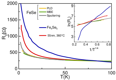
To consider the conjecture that the deformation of the lattice leads to a significant change in the band structure, a crucial point is to determine which is the key physical parameter that quantifies the structural distortion. According to a recent report, there is a correlation between the semimetallic band gap and the in-plane strain in FeSe films ()Phan et al. (2017). However, our epitaxial sample with does not seem to follow this behaviour and is not semimetallic. Therefore, the in-plane strain by itself cannot explain a distortion of the electronic structure. Alternatively, the Poisson’s ratio, , has been proposed to be the parameter that describes insulator-like FeSe epitaxial thin films Hanzawa et al. (2017). To determine if there is a correlation between the insulator behavior and the structural distortion we compare the reported curves of non-superconducting -FeSe samples with the resistivity of our film. First, we consider the reported curves from FeSe thin films fabricated with different growth methods (PLD Molatta et al. (2015), MBE Hanzawa et al. (2016), Sputtering Schneider et al. (2012)) (Figure 8). We found these curves to collapse onto a single curve when normalized by the value at K, indicating a universal behavior. In the case of MBE’s curve (Ref Hanzawa et al. (2016)), . In contrast, our sample, shows a stronger semiconducting feature and has a higher Poisson’s coefficient of . This positive correlation between the Poisson’s coefficient and the semiconducting behavior may be indicative of a strong interplay between the distortion of the lattice and the band structure. Additionally, we included the reported result for Fe4Se5 which has an even higher rise in resistance as the temperature decreases. This implies that the existence of vacancies produces an even more intense effect. In this case, with respect to the relaxed structure . This negative coefficient may be indicative of a non-trivial deformation. Therefore, the intermediate insulating behavior in our sample could be either related to structural distortion and/or a relevant vacancies concentration. Since we did not find a relevant concentration of Fe vacancies, the structural distortion may play the key role.
Regarding the conduction mechanism, there is a linear dependence of with in a wide range of temperature, being the exception the break at K for Fe4Se5 (see the inset in the Figure 8). We emphasize that the dependence is more appropriate than other types of exponents. The mathematical relation is widely used to describe the conductivity in strongly disordered systems with localized states (VRH model). Therefore, the dependence found may suggest a localization effect. The key question is which type of disorder originate the localization. Recently, the formation of potential barriers in the conduction band has been suggested as the origin of the insulator-like behavior Hanzawa et al. (2019). In this scenario, despite a metallic electronic structure observed by ARPES, the carriers cannot move freely due to the influence of the potential barriers.
IV Conclusions
In summary, we have shown that the macroscopic electronic behavior of sputtered FeSe thin films is strongly susceptible to microscopic and mesoscopic characteristics as lattice distortion and/or grain morphology. In the limit of textured thick films, we found optimal superconducting properties (K) at C with a thickness around nm. Characteristics as an enhanced , a relatively high and a low anisotropy are promising features. The enhancement of the critical temperature could be related to a nanoscale intergrowth of -FeSe and -Fe7Se8 and/or stress associated with the coalescence of grains. These samples allowed us to determine the sensitivity of some relevant physical properties to the presence of disorder. Properties like the coherence length and features like the change in the sign of the Hall coefficient concomitant with a positive magnetoresistance are robust to the amount of disorder present in our samples. Strikingly, the Hall effect is linear up to 16T, in contrast to the nonlinear behavior observed below T* in high-quality single crystals.
For epitaxial stressed thin films, the characteristic semimetallic behavior disappears giving rise to an insulating one. We found that the structural distortion, described by the Poisson’s coefficient, may play the key role instead of stoichiometric changes like ordered Fe vacancies. On the other hand, for a less distorted lattice restricted to independent grains, there is also a non-SC behavior. When these grains coalesce, due to thickness increase, superconductivity appears with higher than that for bulk samples. This implies that the superconductor-insulator transition (SIT) induced by reducing the thickness can be understood taking in account the non-trivial evolution of the structural properties and morphology, which can be associated with the strained initial growth of the sputtered -FeSe films.
Acknowledgements.
We thank P. Troyón and M. Corte at CM-GIA-GAATEN-CNEA for SEM/EDX characterization. We also want to thank S. Suarez and P. Pérez for the RBS measurements. Furthermore, we are grateful to M. Sirena and L. Avilés for their help with the AFM characterization. Work partially supported by Conicet PIP 2014-0164, ANPCyT PICT 2014-1265 and Sectyp UNCuyo 06/C441 and 06/C504.References
- Sun et al. (2016) J. P. Sun, K. Matsuura, G. Z. Ye, Y. Mizukami, M. Shimozawa, K. Matsubayashi, M. Yamashita, T. Watashige, S. Kasahara, Y. Matsuda, J. Q. Yan, B. C. Sales, Y. Uwatoko, J. G. Cheng, and T. Shibauchi, Nature Communications 7, 12146 (2016).
- Medvedev et al. (2009) S. Medvedev, T. M. McQueen, I. A. Troyan, T. Palasyuk, M. I. Eremets, R. J. Cava, S. Naghavi, F. Casper, V. Ksenofontov, G. Wortmann, and C. Felser, Nature Materials 8, 630 (2009).
- Nabeshima et al. (2013) F. Nabeshima, Y. Imai, M. Hanawa, I. Tsukada, and A. Maeda, Applied Physics Letters 103, 172602 (2013).
- Imai et al. (2016) Y. Imai, Y. Sawada, D. Asami, F. Nabeshima, and A. Maeda, Physica C: Superconductivity and its Applications 530, 24 (2016).
- Liu et al. (2012) D. Liu, W. Zhang, D. Mou, J. He, Y.-B. Ou, Q.-Y. Wang, Z. Li, L. Wang, L. Zhao, S. He, Y. Peng, X. Liu, C. Chen, L. Yu, G. Liu, X. Dong, J. Zhang, C. Chen, Z. Xu, J. Hu, X. Chen, X. Ma, Q. Xue, and X. J. Zhou, Nature Communications 3, 931 (2012).
- Wang et al. (2012) Q.-Y. Wang, Z. Li, W.-H. Zhang, Z.-C. Zhang, J.-S. Zhang, W. Li, H. Ding, Y.-B. Ou, P. Deng, K. Chang, J. Wen, C.-L. Song, K. He, J.-F. Jia, S.-H. Ji, Y.-Y. Wang, L.-L. Wang, X. Chen, X.-C. Ma, and Q.-K. Xue, Chinese Physics Letters 29, 037402 (2012).
- Lei et al. (2012) H. Lei, D. Graf, R. Hu, H. Ryu, E. S. Choi, S. W. Tozer, and C. Petrovic, Physical Review B 85, 094515 (2012).
- Watson et al. (2015) M. D. Watson, T. Yamashita, S. Kasahara, W. Knafo, M. Nardone, J. Béard, F. Hardy, A. McCollam, A. Narayanan, S. F. Blake, T. Wolf, A. A. Haghighirad, C. Meingast, A. J. Schofield, H. v. Löhneysen, Y. Matsuda, A. I. Coldea, and T. Shibauchi, Physical Review Letters 115, 027006 (2015).
- McQueen et al. (2009) T. M. McQueen, A. J. Williams, P. W. Stephens, J. Tao, Y. Zhu, V. Ksenofontov, F. Casper, C. Felser, and R. J. Cava, Physical Review Letters 103, 057002 (2009).
- Böhmer et al. (2013) A. E. Böhmer, F. Hardy, F. Eilers, D. Ernst, P. Adelmann, P. Schweiss, T. Wolf, and C. Meingast, Physical Review B 87, 180505 (2013).
- Böhmer et al. (2015) A. E. Böhmer, T. Arai, F. Hardy, T. Hattori, T. Iye, T. Wolf, H. v. Löhneysen, K. Ishida, and C. Meingast, Phys. Rev. Lett. 114, 027001 (2015).
- Haindl et al. (2014) S. Haindl, M. Kidszun, S. Oswald, C. Hess, B. Büchner, S. Kölling, L. Wilde, T. Thersleff, V. V. Yurchenko, M. Jourdan, H. Hiramatsu, and H. Hosono, Reports on Progress in Physics 77, 046502 (2014).
- Mazin (2009) B. A. Mazin, AIP Conference Proceedings 1185, 135 (2009).
- Hsu et al. (2008) F.-C. Hsu, J.-Y. Luo, K.-W. Yeh, T.-K. Chen, T.-W. Huang, P. M. Wu, Y.-C. Lee, Y.-L. Huang, Y.-Y. Chu, D.-C. Yan, and M.-K. Wu, Proceedings of the National Academy of Sciences 105, 14262 (2008).
- Chareev et al. (2013) D. Chareev, E. Osadchii, T. Kuzmicheva, J.-Y. Lin, S. Kuzmichev, O. Volkova, and A. Vasiliev, CrystEngComm 15, 1989 (2013).
- Nie et al. (2009) Y. F. Nie, E. Brahimi, J. I. Budnick, W. A. Hines, M. Jain, and B. O. Wells, Applied Physics Letters 94, 242505 (2009).
- Chen et al. (2010) T.-K. Chen, J.-Y. Luo, C.-T. Ke, H.-H. Chang, T.-W. Huang, K.-W. Yeh, C.-C. Chang, P.-C. Hsu, C.-T. Wu, M.-J. Wang, and M.-K. Wu, Thin Solid Films 519, 1540 (2010).
- Tan et al. (2013) S. Tan, Y. Zhang, M. Xia, Z. Ye, F. Chen, X. Xie, R. Peng, D. Xu, Q. Fan, H. Xu, J. Jiang, T. Zhang, X. Lai, T. Xiang, J. Hu, B. Xie, and D. Feng, Nature Materials 12, 634 (2013).
- Song et al. (2011) C.-L. Song, Y.-L. Wang, P. Cheng, Y.-P. Jiang, W. Li, T. Zhang, Z. Li, K. He, L. Wang, J.-F. Jia, H.-H. Hung, C. Wu, X. Ma, X. Chen, and Q.-K. Xue, Science 332, 1410 (2011).
- Schneider et al. (2012) R. Schneider, A. G. Zaitsev, D. Fuchs, and H. V. Löhneysen, Physical Review Letters 108, 257003 (2012).
- Schneider et al. (2013) R. Schneider, A. G. Zaitsev, D. Fuchs, and R. Fromknecht, Superconductor Science and Technology 26, 055014 (2013).
- Speller et al. (2011) S. C. Speller, C. Aksoy, M. Saydam, H. Taylor, G. Burnell, A. T. Boothroyd, and C. R. M. Grovenor, Superconductor Science and Technology 24, 075023 (2011).
- Venzmer, Kronenberg, and Jourdan (2016) E. Venzmer, A. Kronenberg, and M. Jourdan, Journal of Superconductivity and Novel Magnetism 29, 897 (2016).
- Wang et al. (2015) Q. Wang, W. Zhang, Z. Zhang, Y. Sun, Y. Xing, Y. Wang, L. Wang, X. Ma, Q.-K. Xue, and J. Wang, 2D Materials 2, 44012 (2015).
- Pardo, Burmeister, and Guimpel (1996) F. Pardo, G. Burmeister, and J. Guimpel, Review of Scientific Instruments 67, 2370 (1996).
- Kiessig (1931) H. Kiessig, Annalen der Physik 402, 769 (1931).
- Amigó et al. (2017a) M. L. Amigó, M. V. A. Crivillero, D. G. Franco, A. Badía-Majós, J. Guimpel, J. Campo, F. Damay, F. Porcher, A. M. Condó, and G. Nieva, Superconductor Science and Technology 30, 085010 (2017a).
- Werthamer, Helfand, and Hohenberg (1966) N. R. Werthamer, E. Helfand, and P. C. Hohenberg, Physical Review 147, 295 (1966).
- Terashima et al. (2014) T. Terashima, N. Kikugawa, A. Kiswandhi, E.-S. Choi, J. S. Brooks, S. Kasahara, T. Watashige, H. Ikeda, T. Shibauchi, Y. Matsuda, T. Wolf, A. E. Böhmer, F. Hardy, C. Meingast, H. v. Löhneysen, M.-T. Suzuki, R. Arita, and S. Uji, Physical Review B 90, 144517 (2014).
- Amigó et al. (2015) M. L. Amigó, M. V. Ale Crivillero, D. G. Franco, J. Guimpel, and G. Nieva, Journal of Low Temperature Physics 179, 15 (2015).
- Kasahara et al. (2014) S. Kasahara, T. Watashige, T. Hanaguri, Y. Kohsaka, T. Yamashita, Y. Shimoyama, Y. Mizukami, R. Endo, H. Ikeda, K. Aoyama, T. Terashima, S. Uji, T. Wolf, H. von Löhneysen, T. Shibauchi, and Y. Matsuda, Proceedings of the National Academy of Sciences 111, 16309 (2014).
- Amigó et al. (2014) M. L. Amigó, V. Ale Crivillero, D. G. Franco, and G. Nieva, Journal of Physics: Conference Series 568, 022005 (2014).
- Feng et al. (2018) Z. Feng, J. Yuan, J. Li, X. Wu, W. Hu, B. Shen, M. Qin, L. Zhao, B. Zhu, and V. Stanev, arXiv e-prints , arXiv:1807.01273 (2018), arXiv:1807.01273 [cond-mat.supr-con] .
- Lei et al. (2016) B. Lei, J. H. Cui, Z. J. Xiang, C. Shang, N. Z. Wang, G. J. Ye, X. G. Luo, T. Wu, Z. Sun, and X. H. Chen, Phys. Rev. Lett. 116, 077002 (2016).
- Wang et al. (2009) M. J. Wang, J. Y. Luo, T. W. Huang, H. H. Chang, T. K. Chen, F. C. Hsu, C. T. Wu, P. M. Wu, A. M. Chang, and M. K. Wu, Phys. Rev. Lett. 103, 117002 (2009).
- Zhou et al. (2016) G. Zhou, D. Zhang, C. Liu, C. Tang, X. Wang, Z. Li, C. Song, S. Ji, K. He, L. Wang, X. Ma, and Q.-K. Xue, Applied Physics Letters 108, 202603 (2016).
- Amigó et al. (2017b) M. L. Amigó, N. Haberkorn, P. Pérez, S. Suárez, and G. Nieva, Superconductor Science and Technology 30, 125017 (2017b).
- Hanzawa et al. (2016) K. Hanzawa, H. Sato, H. Hiramatsu, T. Kamiya, and H. Hosono, Proceedings of the National Academy of Sciences 113, 3986 (2016).
- Molatta et al. (2015) S. Molatta, S. Haindl, S. Trommler, M. Schulze, S. Wurmehl, and R. Hühne, Scientific Reports 5, 16334 (2015).
- Chen et al. (2014) T.-K. Chen, C.-C. Chang, H.-H. Chang, A.-H. Fang, C.-H. Wang, W.-H. Chao, C.-M. Tseng, Y.-C. Lee, Y.-R. Wu, M.-H. Wen, H.-Y. Tang, F.-R. Chen, M.-J. Wang, M.-K. Wu, and D. Van Dyck, Proceedings of the National Academy of Sciences of the United States of America 111, 63 (2014).
- Phan et al. (2017) G. N. Phan, K. Nakayama, K. Sugawara, T. Sato, T. Urata, Y. Tanabe, K. Tanigaki, F. Nabeshima, Y. Imai, A. Maeda, and T. Takahashi, Physical Review B 95, 224507 (2017).
- Hanzawa et al. (2017) K. Hanzawa, H. Sato, H. Hiramatsu, T. Kamiya, and H. Hosono, IEEE Transactions on Applied Superconductivity 27, 1 (2017).
- Hanzawa et al. (2019) K. Hanzawa, Y. Yamaguchi, Y. Obata, S. Matsuishi, H. Hiramatsu, T. Kamiya, and H. Hosono, Phys. Rev. B 99, 035148 (2019).