Probing the limits of the rigid-intensity-shift model in differential phase contrast scanning transmission electron microscopy
Abstract
The rigid-intensity-shift model of differential phase contrast scanning transmission electron microscopy (DPC-STEM) imaging assumes that the phase gradient imposed on the probe by the sample causes the diffraction pattern intensity to shift rigidly by an amount proportional to that phase gradient. This behaviour is seldom realised exactly in practice. Through a combination of experimental results, analytical modelling and numerical calculations, we explore the breakdown of the rigid-intensity-shift behaviour and how this depends on the magnitude of the phase gradient and the relative scale of features in the phase profile and the probe size. We present guidelines as to when the rigid-intensity-shift model can be applied for quantitative phase reconstruction using segmented detectors, and propose probe-shaping strategies to further improve the accuracy.
I Introduction
Samples in transmission electron microscopy (TEM) impart phase shifts on the electron beam that passes through them. These phase shifts follow from the Aharonov-Bohm effect Aharonov and Bohm (1959) and thus encode information on the electric and magnetic fields within the sample. Longer range (nm–m) fields include those caused by magnetic domains and in-built electric fields within semiconductor devices. Within the projection and phase object approximations Vulović et al. (2014); Brown et al. (2017) – often valid for typical electron acceleration voltages (80–300 keV) and sample thicknesses (which at lower resolution might extend to 100 nm) Nellist and Pennycook (2011) – the exit surface wavefunction, , is related to the entrance surface wavefunction, , via multiplication with a transmission function, :
| (1) | |||||
where describes the sample-induced phase shift. This imparted phase is lost if the exit wavefunction is imaged in focus, but a range of techniques exist that convert this imparted phase to measurable intensity changes.
In conventional TEM, where the entrance wavefunction is a plane wave, weak phase shifts (much less than ) can be visualised using Zernike phase-contrast Born and Wolf (1999); Malac et al. (2017); Danev et al. (2014) or out-of focus (Lorentz) imaging De Graef and Zhu (2000); Petford-Long and Chapman (2006); Phatak et al. (2016). For the stronger phase shifts usually pertaining to materials specimens Beleggia (2008); Vulović et al. (2014), techniques include through-focal series phase retrieval Coene et al. (1992); Allen et al. (2004) and off-axis holography Dunin-Borkowski et al. (2015). A strength of conventional TEM is synchronous acquisition of the full field of view: images are recorded with perfect registration between pixels.
In scanning-TEM (STEM), the electron beam is focussed into a small probe at the sample entrance surface by a set of condenser lenses and apertures, of which the final aperture, characterised by its convergence semiangle, , determines the probe size at the sample Williams and Carter (1996). The probe is then scanned across the specimen, with the STEM image(s) built up by plotting the recorded signal(s) as a function of probe position. This serial acquisition over probe positions can introduce image distortions, but allows for multiple images to be recorded in perfect registration to one another. This makes STEM a powerful technique for correlative imaging.
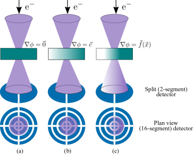
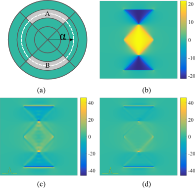
Fig. 1a depicts the convergent probe incident upon a sample that imparts a constant phase shift, with the effect that the intensity distribution in the far-field (also called the diffraction plane) is an image of the probe-forming aperture, called the bright-field disk. Fig. 1a further depicts this bright-field disk falling on example configurations of multiple detectors (split detector in profile view; segmented detector in plan view). This subdivision of the detector plane allows direct imaging of the phase gradient via differential phase contrast (DPC), as first suggested and implemented in the 1970s Rose (1974); Dekkers and De Lang (1974). The essence of this approach is shown in Figs. 1b and c. In classical terms the Lorentz force from an electric field that is perpendicular to the optical axis, or in wave-optical terms a transverse gradient in the imparted phase, deflects the beam laterally. If the detector comprises multiple, non-rotationally-symmetric elements, this redistribution of the intensity in the diffraction plane (the diffraction pattern) can be measured using the difference in recorded intensity on the different detector segments.
In the wave-optical formulation, the diffraction pattern intensity can be described using Eq. (1) as:
| (2) | ||||
| (3) |
where denotes convolution and denotes Fourier transform with respect to and , and and are the corresponding Fourier-space coordinates. If the gradient of the imparted phase is strictly linear over the full width of the incident wavefunction, the Fourier shift theorem implies a rigid deflection of the diffraction pattern Goodman (2005); Lubk and Zweck (2015); Lazić et al. (2016), as depicted in Fig. 1b. Conversely, when the gradient of the imparted phase varies across the incident wavefunction, the exact rigid-intensity-shift model is not expected to hold Müller et al. (2014); Lazić et al. (2016); Cao et al. (2017) and the intensity in the diffraction pattern will be redistributed in a more complex fashion, as depicted in Fig. 1c. DPC imaging is often conceptualised in terms of the diffraction pattern undergoing a rigid intensity shift (also called rigid disk shift since in the absence of more complex intensity redistribution the diffraction pattern is disk shaped) – especially so for the case of longer-range field imaging Chapman et al. (1992); Lohr et al. (2012); Zweck et al. (2016); Krajnak et al. (2016); Lohr et al. (2016); Schwarzhuber et al. (2017); Wu and Spiecker (2017). In many microstructured materials, however, the phase gradient varies across the illuminated specimen region and so the rigid-intensity-shift model may not hold exactly. A particular example of interest, which we revisit and extend presently, was given in the p-n junction DPC-STEM imaging work of Shibata et al. Shibata et al. (2015).
The breakdown of the rigid-intensity-shift model is exacerbated by the long tails of the STEM probe intensity. In the absence of lens aberrations the entrance wavefunction in STEM is given by:
| (4) |
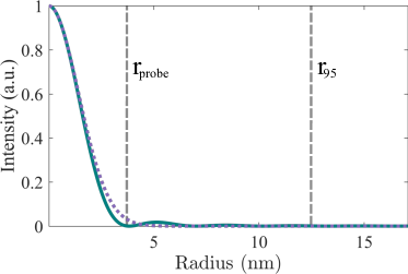
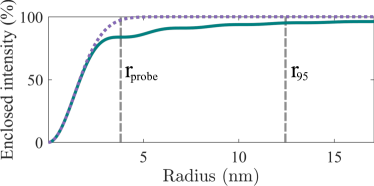
where is an intensity normalisation, , is a first-order Bessel function of the first kind, and . Such a probe is well known, comprising a central Airy disc, and surrounded by weaker rings with intensities decreasing slowly with radius. This is shown as an intensity profile in Fig. 2a. In STEM imaging, the probe size is typically referred to as , the radius of the central disc. However, as shown in the enclosed intensity plotted in Fig. 2b, this central disc contains only % of the probe intensity. The remaining intensity is broadly distributed, as demonstrated by comparison with a Gaussian probe of the same full-width at half-maximum (FWHM) Born and Wolf (1999); McKechnie (2016). If instead we define the probe radius as , the radius which contains % of the probe intensity, the potential for inaccurate data interpretation in DPC-STEM becomes clear: the probe has a much larger spatial extent in real space than is typically accounted for.
For atomic resolution STEM imaging, the gradient of the phase profile imparted by individual atomic columns varies significantly across the incident wavefunction of even the narrowest aberration-corrected STEM probes, where the resultant elaborate diffraction pattern intensity redistribution is widely appreciated. Analysis methods that are suited to this regime and exploit recent improvements in high-speed pixellated detectors Tate et al. (2016); Yang et al. (2016) include first-moment-detector DPC-STEM Waddell and Chapman (1979); Müller et al. (2014); Lubk and Zweck (2015); Lazić et al. (2016); Müller-Caspary et al. (2017); Lazić and Bosch (2017); Cao et al. (2017)and ptychography Faulkner and Rodenburg (2004); Morgan et al. (2013); D’Alfonso et al. (2014); Yang et al. (2016). While these new detectors seem promising, at present they remain specialist systems which produce extremely large datasets Lazić and Bosch (2017) and do not readily allow live imaging (i.e. at the few-second refresh rate of experimental scans) to find structural features of interest and optimise the probe aberrations. One compromise is a segmented detector system, as depicted in Fig. 1, which uses more established technology, allows for faster scans and produces more manageably-sized data sets. For strong phase objects, segmented detectors can give a very good approximation to the diffraction pattern centre-of-mass Lazić et al. (2016); Close et al. (2015); Lazić and Bosch (2017). For weak phase objects, they allow for linear reconstructions Landauer et al. (1995); McCallum et al. (1995); Majert and Kohl (2015); Pennycook et al. (2015); Seki et al. (2017).
While these more elaborate segmented detector analysis methods can be applied to long range fields Brown et al. (2017), the rigid-intensity-shift model has much to recommend it in addition to its conceptual simplicity. Zweck et al. used its analytical tractability to establish clear guidelines for achievable field sensitivity Zweck et al. (2016); Schwarzhuber et al. (2017). Experimental calibration Shibata et al. (2015); Schwarzhuber et al. (2017); Wu and Spiecker (2017) enables simple implementation and analysis, and can largely account for inelastic scattering effects from thicker samples Brown et al. (2017). In this paper we seek to better understand the diffraction pattern intensity redistribution in objects with long-range fields, to establish the domain of validity of the rigid-intensity-shift model of DPC-STEM, and to explore the manner in which it breaks down 111Chapman et al. Chapman et al. (1978) explored this question in the context of domain wall imaging by Taylor expanding the imparted phase of Eq. (1) to second order. Appropriate to the instrumentation of the time, the first order correction to the rigid-shift model depended on lens aberrations but vanishes in an aberration-free system. The current generation of aberration corrected STEM instruments offer greater control over lens aberrations, and a particular strength of DPC-STEM is that it can be done in-focus, usually the optimum imaging conditions for other STEM imaging modes (such as high-angle annular dark-field Williams and Carter (1996)) that one might wish to acquire simultaneously Shibata et al. (2015, 2017)..
This paper is organised as follows. In Sec. II, a p-n junction in a Gallium Arsenide (GaAs) specimen is explored as a case study of a phase profile varying in one dimension (i.e. is a function of alone), using both experimental data and an analytical model to investigate realistic limits to the rigid-disk-shift model of DPC-STEM. A simulation study of magnetic diamond domains in a Nickel-Iron (NiFe) specimen is explored as a case study of a 2D-varying phase profile in Sec. III. These case studies demonstrate that while the rigid-intensity-shift model does not exactly hold, for imaging long range fields the more complex intensity redistribution occurs predominantly near the edges of the diffraction pattern. As such, Sec. IV explores the precision obtainable for quantitative field imaging with a segmented detector when analysed in the rigid-intensity-shift model. Since the extent of STEM probe tails is shown to be a limiting factor, Sec. V proposes a beam shaping strategy to extend the validity of the rigid-intensity-shift model.
II 1D-varying phase profile case study: junction in
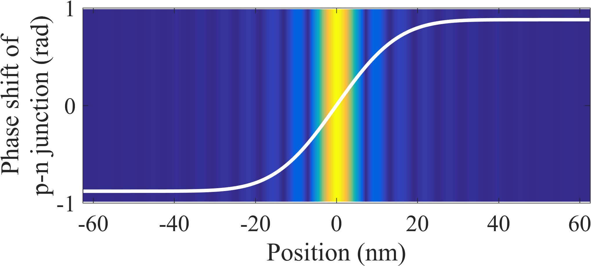
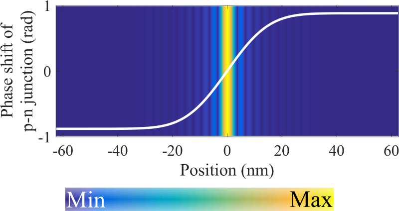
Here we revisit and extend the previously-examined case of a 290 nm thick, slab-like specimen of GaAs with symmetrical p-n junction between cm-3 p-doped (Zn) and cm-3 n-doped (Si) regions Shibata et al. (2015); Brown et al. (2017). For this system, the transmission function describing the phase profile imparted by the intrinsic electric field across the junction is well-approximated by the 1D function Shibata et al. (2015):
| (5) |
where is the interaction constant (7.29 (Vnm)-1 for 200 keV electrons) De Graef (2003), nm is the (deduced) active-region thickness, eV is the difference in mean inner potential between the p- and n-doped regions of the semiconductor material, and nm is the characteristic width of the junction (numerical values as determined in Ref. Shibata et al. (2015)).
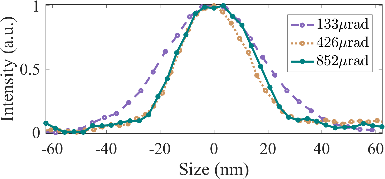
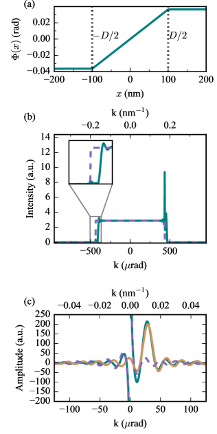
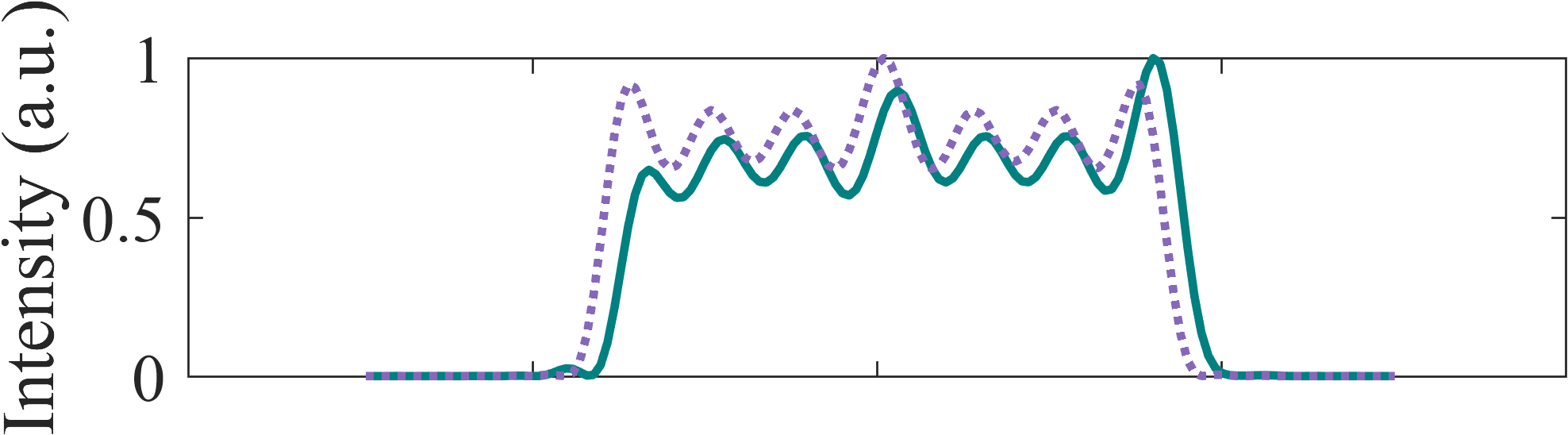
In seeking to understand the limits of the rigid-disk-shift model, we illuminated this specimen with three different probe sizes, characterised by convergence semiangles 133, 426 and 852 rad, the scaling of which are shown in comparison to that of the phase profile of the transmission function of the junction in Figs. 3a, 3b, and 3c, respectively 222In contrast to Fig. 2, the probe amplitude, , is shown here to emphasise the extent of the probe tails.. The rad case produces the broadest probe, and is that used previously Shibata et al. (2015); Brown et al. (2017) for which the diffraction pattern showed an intensity redistribution more complex than a simple rigid intensity shift. This followed because the widths of the p-n junction and probe intensity distribution are comparable: the phase gradient varies appreciably across the central intensity lobe of the probe distribution, as seen in Fig. 3a. We might therefore expect that the finer probes, for which Figs. 3b and 3c show less variation in the phase gradient across the region of appreciable intensity, would better justify the rigid-disk-shift model. This expectation is reinforced by the DPC-STEM profiles in Fig. 3d which converge to essentially the same profile for the two narrower probes.

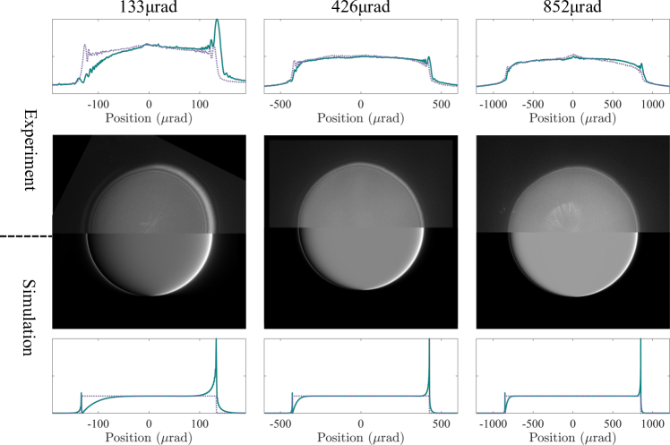
The detailed diffraction pattern distributions, however, show that the scattering physics is not so simple. Figure 4 compares diffraction patterns between experiment and simulation (using Eq. (3)) for the three different convergence semiangles. The intensity profiles, taken from across the centre of the full diffraction patterns, compare on-junction to off-junction results. The experimental and simulated patterns are in broad qualitative agreement. (The Fresnel fringing and other fine structure evident in the experimental patterns result from the images having been recorded on photographic film and so containing residual aberrations that were not able to be identified and minimised during recording.) A rigid-disk-shift model would predict a shift of approximately 18 rad (based on the field strength at the centre of the junction), but the patterns make clear that none of the on-junction patterns are simply rigidly shifted versions of their off-junction counterparts. Rather, each pattern shows a bright-intensity peak on the right hand edge of the disk, and a reduced-intensity trough on the left hand edge of the disk, at diffraction-plane positions broadly within the same area as that illuminated in the off-junction case. Indeed, although these peak and trough features constitute a smaller fraction of the diffraction pattern for increasing convergence semiangle, their angular extent is the same in each case.
To better understand these features, let us consider a piecewise approximation to Eq. (5) that is amenable to analytic manipulation. Assuming a constant electric field within the p-n junction and zero electric field outside, the transmission function may be written:
| (6) |
where is the nominal width of the junction and . Note that is different to the characteristic width, , in the error function model of Eq. (5). For nm, a value of nm minimizes the root-mean-square error between this piecewise approximation and the error function model, the comparison is shown in Fig. 5a(i).

Equation (6) can be rewritten in terms of functions commonly found in tables of Fourier transforms:
| (7) |
where is the sign function and is the rectangle function given by:
| (8) |
The first two terms in Eq. (7) are only non-zero for and so pertain to the field-free region of the specimen. The final term is only non-zero for and so pertains to the region of the specimen where the electric field is constant. Fourier transformation of Eq. (7) gives:
| (9) |
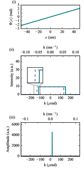
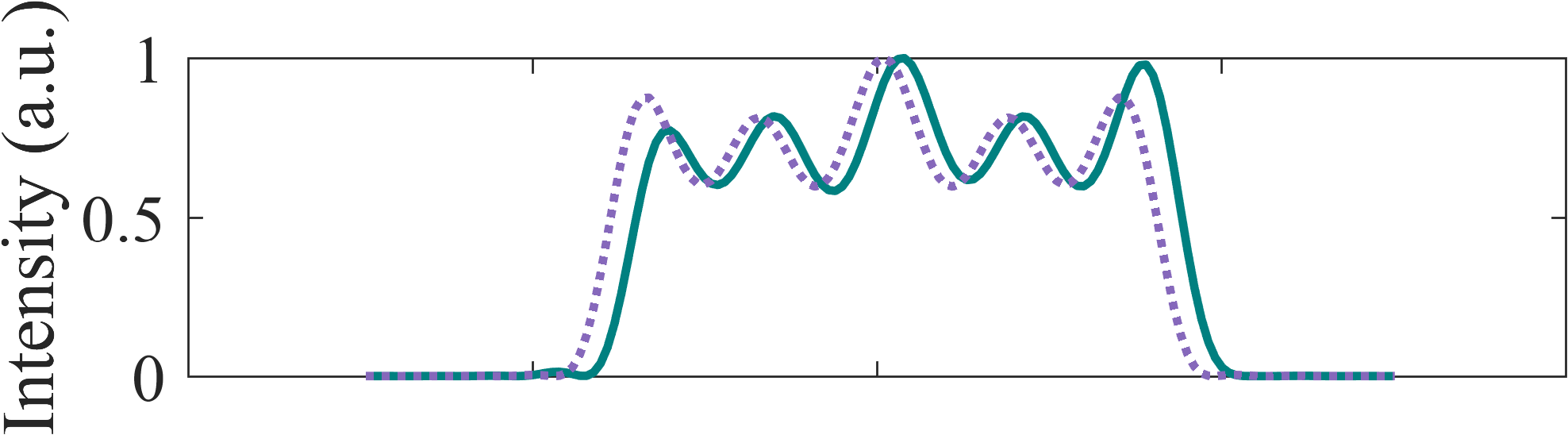
With reference to Eq. (3), the diffraction plane wavefunction of the scattered probe is given by the convolution of Eq. (9) with the reciprocal space illumination wavefunction (the aperture function). In 1D, the aperture function is a top-hat and, for comparison with the experiments, we have set the width to be rad. The resulting diffraction pattern is shown in Fig. 5a(ii) as a teal, solid line. For reference, the reciprocal-space form of the entrance wavefunction intensity , the aperture function, is also shown as a lilac, dotted line. It can be seen that the simplified analytic model qualitatively accounts for the features of the diffraction pattern plotted in Fig. 4 for the rad case, which used the error function model for the phase of the p-n junction transmission function. Different components of Eq. (9) are plotted in Fig. 5a(iii). Before discussing these in detail, it is helpful to consider two limiting cases.
The third term in Eq. (9), , corresponds to the region of constant electric field in Eq. (6) and accounts for a shift in the diffraction pattern centre of mass due to the transverse electric field of the specimen. In the limit , this term will approach a -function (i.e. cause a rigid shift of the illumination). Figure 5b(i) plots the transmission function phase assuming the limiting case of a very large p-n junction with the same built-in electric field ( rad/nm). This causes the diffraction pattern to shift rigidly to the right (by nm-1 or 14.6 rad), as shown in Fig. 5b(ii). The Fourier transform of the transmission function is seen to essentially be a -function, Fig. 5b(iii).
In the limit , but with scaled such that is constant, Eq. (9) approaches:
| (10) |
Here it is possible to derive an analytic expression for the diffraction pattern:
| (11) |
Setting rad, to produce the same potential difference as that across the p-n junction in Fig. 5a(i), gives the step-function transmission function phase shown in Fig. 5c(i). The diffraction pattern resulting from Eq. (11) is plotted in Fig. 5c(ii). The most pronounced features in this diffraction pattern are the sharp peaks at , i.e. at the edges of the aperture function, resulting from the logarithmic divergence in Eq. (11). Note that is the only meaningful length scale in this limit, and as such the intensity both within and spreading beyond the aperture function varies on this scale. Figure 5c(iii) plots the transmission function , showing the divergence inherent in the factor in the second term of Eq. (10). This establishes why the points of divergence in the diffraction pattern occur at the edges of the aperture function: in convolving the top-hat function with this transmission function, those are the points where the top-hat overlaps only one half of the divergence.
Figure 5b and the associated discussion showed how the term in Eq. (9) gives rigid-intensity-shift behaviour. Similarly, Fig. 5c and the associated discussion showed how the term in Eq. (9) leads to the sharp peaks at the edges of the aperture function. These observations aid interpretation of the relative contribution of the different terms in Eq. (9) to the diffraction pattern shown in Fig. 5a(ii) resulting from the piecewise approximate p-n junction potential. Figure 5a(iii) explores the relative contributions of the second and third term in Eq. (9). The transmission function is plotted as a teal, solid line; the second term, , as a lilac, dashed line; and the third term, the term, as the mustard, solid line.
It can be seen that as due to the factor in the second term in Eq. (9), which necessarily dominates for sufficiently small and, as seen in discussion of Fig. 5c, leads to sharp intensity peaks at the edges of the aperture function in Fig. 5a(ii), again the dominant feature of the diffraction pattern. Note, however, that there is now an additional length scale in the problem: the junction width, . Through the factor in the second term in Eq. (9), this has the effect of making the intensity peaks at the edges of the aperture function in Fig. 5a(ii) narrower than those of Fig. 5c(ii).
While in the limit in Fig. 5b(iii) the term containing the rigid shift tendency was both -function like and dominant, in Fig. 5a(iii) it has finite width (of order ) and the shift of the central peak is hidden within the divergence of the term. The former means that the width of the intensity variation in the extended peak-trough feature is about nm-1, or about 60 rad, consistent with Fig. 5a(ii). The latter means that the shift of the diffraction pattern intensity is obscured by the peak-trough feature.
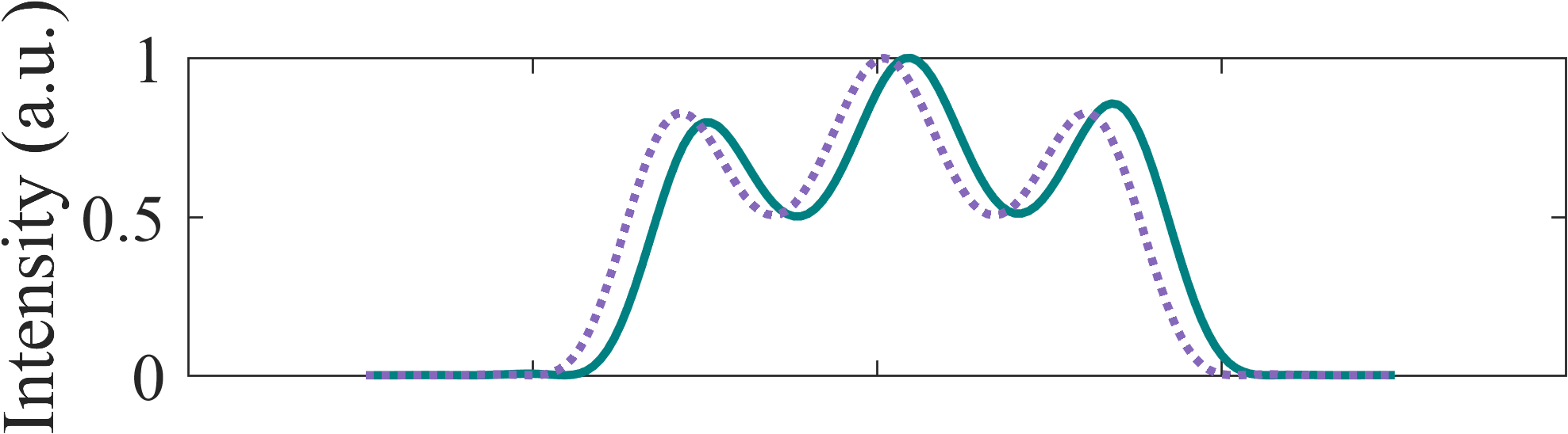
It is also instructive to consider a case where the rigid-disk-shift model is known to be a good approximation. Krajnak shows model data from a polycrystalline magnetic sample which imposes a linear phase gradient of rad/nm on the wavefunction in a region that extends for 200 nm, which is much larger than the probe ( nm for a 436 rad probe forming aperture at 200 keV) Krajnak (2017). Figure 6a is the same as Fig. 5a(i) except that parameters pertinent to the Krajnak model have been used. As can be seen in Fig. 6b, especially in the magnified inset, the intensity distribution in the diffraction pattern is rather well described by the rigid-disk-shift model, though on close inspection small intensity peaks at the edge of the aperture function are still evident.
We can understand this qualitative difference from Fig. 6c, which explores the relative contributions of the second and third term in Eq. (9). Again, as because the factor in the second term necessarily dominates for sufficiently small , explaining the small intensity peaks at the edge of the aperture function. Note, however, that these terms are smaller and narrower than the intensity peaks in Fig. 5a(ii) because the factor in the second term oscillates rapidly (due to the large value of ) 333These rapid oscillations might also be considered an example of the well-known Gibbs phenomenon Goodman (2005) where if even a generous bandwidth limit is applied to a step discontinuity then high frequency oscillations will result near the discontinuity. Here, the factor in the transmission function in Eq. (7) acts as a bandwidth limit on the shifted component of the probe.. It is likely that such oscillations would be challenging to observe experimentally, even on state-of-the-art instruments, due to finite beam coherence and detector resolution, and further complicated by such oscillations being similar in form to Fresnel fringes resulting from imperfect focussing. Also in contrast to Fig. 5a(iii), the term containing the rigid-shift tendency is much narrower (because is smaller) and is clearly separated from the divergence point of the second term. That the magnitude of the shift in is larger than the length scale on which the diffraction pattern intensity varies means that there is now a dominating shift of the diffraction pattern intensity.
The shift, , in the third term in Eq. (9) will be greater than the length scale on which the diffraction pattern intensity varies if:
| (12) |
Noting that in the ideal rigid-disk-shift case the detected deflection angle, , can be related to the imparted phase gradient (for small deflections) via Krajnak (2017); Zweck et al. (2016):
| (13) |
Equation (12) can also be written as:
| (14) |
where is the scattering angle scale of the intensity redistribution at the edge of the diffraction patterns. It is also interesting to note that recognising the mean momentum transfer to the probe as and the size of the junction as , then Eq. (12) becomes analogous to the quantum mechanical Heisenberg uncertainty principle:
| (15) |
By comparing the size of the different probes against the p-n junction in Fig. 3 we anticipated that, while the phase gradient varied appreciably on the scale of the rad probe, the much narrower rad probe would have shown a more rigid-intensity-shift-like behaviour. However, this was not supported by the experimental and simulated results in Fig. 4. The additional conditions of Eqs. (12) and (14) explain this: the deflection expected from the peak field strength in the p-n junction is rad, which is smaller than the length scale on which the diffraction pattern intensity varies, rad. This requirement is fundamental to the object but independent of the probe forming aperture, which is why forming a finer probe failed to make the scattering more rigid-shift like in Fig. 4. Conversely, in the Krajnak example, rad is appreciably larger than rad, hence the rigid-intensity-shift model holds better.
We now seek to broaden our understanding through a study of a more complex specimen geometry where varies in both and .
III 2D-varying phase profile case study: magnetic domains in
DPC-STEM has been particularly useful for studying magnetic microstructure Chapman et al. (1990); Chapman (1984); Uhlig and Zweck (2004); Uhlig et al. (2005). As such, phase gradients imposed by magnetic domains are a highly relevant model system. Here we work with a simulated specimen of NiFe, with magnetisation vectors generated using the Object Oriented MicroMagnetic Framework (OOMMF) software developed at the National Institute of Standards and Technology (NIST) Donahue and Porter (1999). A standard soft magnetic material was modelled using anisotropy constant, J/m3, saturation magnetization, kA/m, and exchange coefficient, pJ/m.
The magnetisation vectors were converted to transmission function phase shifts following Refs. De Graef et al. (1999); Dunin-Borkowski et al. (2015), and interpolated to match the real-space requirements for adequately-sampled STEM diffraction calculations. The electric potential is assumed constant. The phase distribution imparted by this structure is illustrated in Fig. 7a. The crosses indicate the probe positions at which the diffraction patterns shown in Fig. 7b were calculated, assuming a rad convergence semiangle.
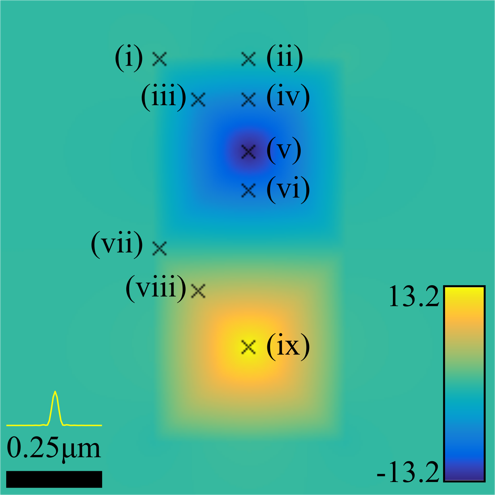
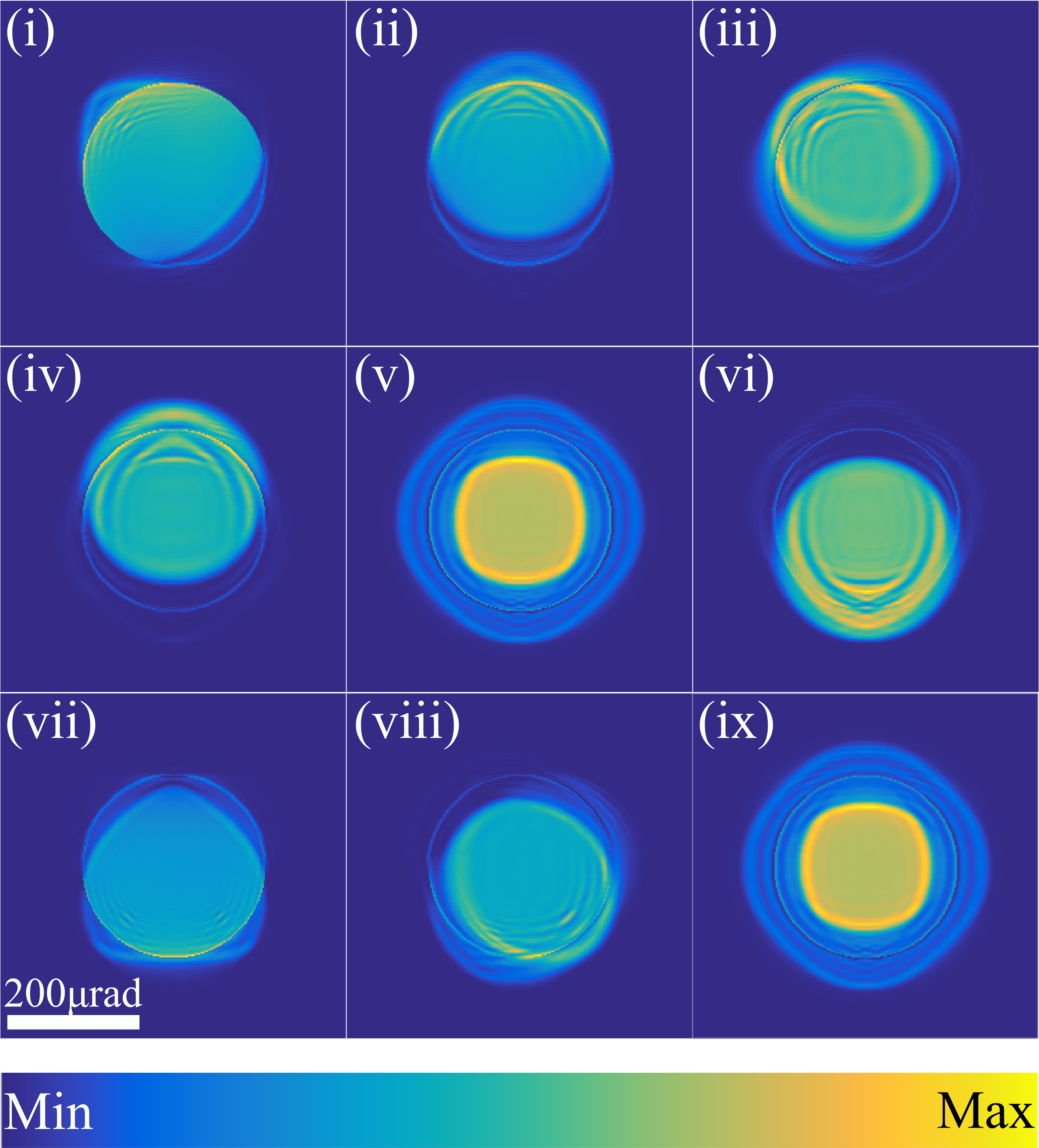
In these diffraction patterns, a number of features are visible. Diffraction patterns (i) and (iii) both show the diagonal symmetry of the the phase profile at their respective probe positions, but with more severe peak-trough features in (iii) as more of the probe is sitting over regions of non-constant . Diffraction patterns (ii), (iv) and (vii), with the least variation in phase gradient under the centre of the probe, show a general trend of intensity shift from their central position, but are still decorated with substantial intensity redistributions. Fig. 7b(v) and (ix) are rather similar – the probe positions have the same local symmetry though the phase profiles have opposite sign. When varies dramatically under the central region of the probe, the intensity redistributions of the diffraction pattern become more severe.
The diffraction patterns in Fig. 7b show sharp peak-trough type features not unlike those seen earlier in Fig. 4: such features are not exclusive to the simple 1D-varying phase profile case but rather occur over a variety of systems and probe positions. The generality of these features means that the rigid-intensity-shift model will rarely be exactly realised. If the diffraction patterns in Fig. 7b were recorded on a pixel detector, the deviation from the rigid-intensity-shift model might itself be used to extract information about the structure. If instead a segmented detector were used, the deviation from the rigid-intensity-shift model would be hard to gauge from the STEM images alone. However, this loss of sensitivity to fine intensity redistribution may not necessarily be a great limitation: if the intensity redistribution is sufficiently localised within the detector segments then a rigid-intensity-shift analysis applied to segmented detector DPC-STEM may be a good approximation. To explore this, we now compare the true phase gradient of Fig. 7a with that estimated by a segmented detector.
IV Effect of intensity redistributions on segmented detector DPC-STEM accuracy
Assuming a rigid-disk-shift model, segmented detector STEM images can be used for quantitative phase gradient measurement via a calibration establishing the correspondence between the signal in the various detectors and the magnitude and direction of the disk deflection. Majert and Kohl Majert and Kohl (2015) present analytic expressions for deflected bright-field disk overlap with detector segments. Alternatively, the calibration can be carried out experimentally Shibata et al. (2015); Zweck et al. (2016); Schwarzhuber et al. (2017); Brown et al. (2017), which has the advantage of accounting for the realistic detector response and some spreading of the bright-field disk via inelastic scattering.
Our simulations were set up as follows. To emulate the experimental set-up used to obtain Fig. 3(d), the detector was oriented as indicated in Fig. 8(a), with camera length chosen such that the bright-field disk extends to midway through the third ring of detector segments. To calibrate phase measurements of , for each convergence semiangle considered a look-up table was generated relating the difference in intensity recorded in segment A and segment B (see Fig. 8(a)) to the actual bright-field disk shift. Note that a more elaborate approach, perhaps based on approximate centre of mass, would be needed to handle deflections which shift the bright-field disk completely off either of segments A or B. Fig. 8b shows for the magnetic domain structure of Fig. 7(a). For convergence semiangles of rad and rad respectively, Figs. 8c and d show the difference between the calibrated segmented detector DPC-STEM estimate for and the true value.
The segmented detector measurement of the phase gradient is least accurate near to regions of phase gradient change (most significantly at the top and bottom edges of the sample). However, in Fig. 8c further differences are perceptible as more subtle ripples lying horizontally across the domains in the difference image. These are regions where the true phase gradient is linear, but peaks and troughs in the diffraction patterns pass on and off the detector segments, as a result of the broad probe tails. The dynamics of this rippling behaviour are shown in more detail in supplementary video A.
In Fig. 8d, the differences are more localised to regions of strong phase gradient change. As previously seen in Fig. 4, changing the convergence semiangle does not necessarily alter the angular extent of the intensity redistribution at the edges of the bright-field disk. However, because we assume camera lengths such as to maintain the same geometric overlap between the detector segments and the bright-field disk, as the convergence semiangle increases the intensity redistribution on the edges of the bright-field disk become more localised with respect to the detector segments. This is shown in supplementary video B.
Fig. 8c and d show the typical error is of the order of of the signal. The largest errors are strongly localised to specific features. For most of the imaged area the errors remain small: segmented detector DPC-STEM can give good quantitative results even when, as shown in Sec. II and III, there are significant deviations away from a rigid disk shift.
V Effect of probe shaping on segmented detector DPC-STEM accuracy
The analytic modelling in Sec. II and the ripples in the difference map in Fig. 8(c) suggest that much of the remaining discrepancies are attributable to the long probe tails. It follows that if the interrogating probe can be reshaped to minimise the breadth and intensity of the probe tails then the accuracy of quantitative segmented detector DPC-STEM would improve further still.
Novel electron probe shaping has become feasible over the last few years, primarily in conjunction with studies into electron vortex beams Bliokh et al. (2017); Verbeeck et al. (2010); McMorran et al. (2011); Lloyd et al. (2017); McMorran et al. (2017). A number of routes to shape electron probes were developed, including manipulating optical aberrations Clark et al. (2013); Petersen et al. (2013), exploiting the mean inner potential of materials Shiloh et al. (2014); Béché et al. (2016) and using nanoscale magnetic fields Béché et al. (2014); Blackburn and Loudon (2014). In particular, as it is now possible to produce probes that do not have the long probe tails of the Airy-probe, we investigate the effect of reduced probe tail width on the quantitative accuracy of segmented detector DPC-STEM.
A simple probe shape with reduced tail intensity is a Gaussian probe, cf. Fig. 2. The literature gives two different routes to creating such a probe. Recent work by McMorran et al. has used electron phase plates to form a Gaussian wavefront directly McMorran . A less elegant method – but one perhaps simpler to employ since such phase plates are not yet widely available and inserting them into electron microscopes is non-trivial – would be to use judicious combinations of the several condenser apertures typically available in the microscope. A first condenser aperture would create the standard Airy-disk electron probe, and a later (but still pre-sample) aperture could be used to truncate the probe at a minimum of the Airy disk. Such probe truncation (as a simple example of apodisation) is well known in astronomy and visible light optics and can produce a good approximation to a Gaussian beam Born and Wolf (1999); Jacquinot and Roizen-Dossier (1964).
We return to the p-n junction case, Eq. (5), to demonstrate the changes in the diffraction plane caused by successive apodisations of the Airy probe. Fig. 9 shows simulated intensity profiles of the diffraction pattern when the probe illuminates the centre of the p-n junction and is apodised at the , , and Airy minima. As compared with the top-hat diffraction intensity profile of an unapodised probe, the increasingly narrow apodisation is seen to make the profile more Gaussian (the expected form of the diffraction pattern of a Gaussian probe). In Fig. 9(a), left-right asymmetry within the diffraction pattern is evident, echoing much of the behaviour of Fig. 4. The central position of the diffraction pattern intensity may be somewhat shifted, but the intensity redistribution between the off-junction and on-junction cases is not a simple rigid shift. However, as the apodisation radius becomes increasingly narrow, the intensity redistribution within the disc decreases in significance, and the shift of the diffraction pattern becomes clearer – the behaviour predicted by the initial rigid-disk-shift model. In Fig. 9(d), the on-junction intensity is a simple shifted version of the off-junction intensity.
To explore whether this probe shaping improves the accuracy of quantitative segmented detector DPC-STEM, we turn again to the magnetic domain case study of Sec. III and IV. Over a series of convergence semiangles (rad, rad and rad) and apodisation cutoffs (at the , and Airy minima), segmented detector simulations were performed to find the phase gradients obtained. The difference between these measured and true phase gradients, depicted in Fig. 10, show increasing localisation of the sample regions that are not accurately reconstructed – the tails have a decreasing effect as the apodisation strength is increased.
The reconstructed phases for the probes apodised at the first Airy minimum closely match the true phase gradient, aside from when the probe is within of a strong change in phase gradient. Reducing probe tails does indeed seem to be a promising way to improve the quantitative accuracy of segmented detector DPC-STEM.
VI Conclusion
In this study, the break down of the rigid-intensity-shift model of DPC-STEM when the gradient of the imparted phase varies across the incident wavefunction, previously anticipated in principle and explored in the atomic resolution regime Müller et al. (2014); Lazić et al. (2016); Müller-Caspary et al. (2017); Cao et al. (2017), has been explored in detail for imaging long-range fields. Combining experimental, analytic modelling and simulations, we have shown that the breaking of this model is quite generic, and occurs for a range of specimen and probe parameters. It is worth stressing that this occurs in simple phase objects; it does not require dynamical scattering.
Whether applying rigid-disk-shift interpretation is valid depends on the relationship between properties of the specimen, detector and probe. Our conclusions can be summarised as follows:
(A) The diffraction pattern intensity redistribution will not be well described in detail by a rigid-disk-shift interpretation, irrespective of probe size, unless the product of the phase gradient and the length over which it is constant is sufficiently large (see Eq. (12)).
(B) If the convergence semiangle is sufficiently large compared to the feature size, the diffraction pattern intensity redistribution may nevertheless be confined within a detector segment, allowing an accurate, quantitative DPC-STEM reconstruction using the simple rigid-disk-shift model.
(C) As deviations from the rigid-disk-shift model are exacerbated by the broad tails of Airy probes, probe reshaping to reduce these tails can enable quantitative, accurate DPC-STEM reconstruction for a broader range of specimens.
If the diffraction patterns were recorded on a pixel detector, the break down of the rigid-intensity-shift model is not particularly problematic and may even be used to extract information about the structure. However, that approach produces enormous data sets (on the order of data points per probe position) and requires complicated analysis. Our results show that judicious use of convergence angle and probe shaping enables quantitative, accurate phase reconstruction to be achieved using STEM images recorded on just a few detector segments. This permits faster data collection and produces datafiles of easily manageable size, which is highly attractive for high-throughput practical applications.
Acknowledgements.
This research was supported by the Australian Research Council Discovery Projects funding scheme (Project DP160102338). N.S. acknowledges support from SENTAN, JST and JSPS KAKENHI Grant numbers JP26289234 and JP17H01316. The GaAs p-n junction samples were provided by Hirokazu Sasaki, Furukawa Electric Co., Ltd.References
- Aharonov and Bohm (1959) Y. Aharonov and D. Bohm, Phys. Rev. 115, 485 (1959).
- Vulović et al. (2014) M. Vulović, L. M. Voortman, L. J. van Vliet, and B. Rieger, Ultramicroscopy 136, 61 (2014).
- Brown et al. (2017) H. G. Brown, N. Shibata, H. Sasaki, T. C. Petersen, D. M. Paganin, M. J. Morgan, and S. D. Findlay, Ultramicroscopy 182, 169 (2017).
- Nellist and Pennycook (2011) P. D. Nellist and S. J. Pennycook, Scanning Transmission Electron Microscopy: Imaging and Analysis (Springer, 2011).
- Born and Wolf (1999) M. Born and E. Wolf, Principles of Optics, 7th (expanded) edition (Cambridge University Press, 1999).
- Malac et al. (2017) M. Malac, E. Kano, M. Hayashida, M. Kawasaki, S. Motoki, R. Egerton, I. Ishikawa, Y. Okura, and M. Beleggia, Microsc. Microanal. 23, 842 (2017).
- Danev et al. (2014) R. Danev, B. Buijsse, M. Khoshouei, J. M. Plitzko, and W. Baumeister, PNAS 111, 15635 (2014).
- De Graef and Zhu (2000) M. De Graef and Y. Zhu, eds., Magnetic Imaging and Its Applications to Materials, Vol. 36 (Elsevier, 2000).
- Petford-Long and Chapman (2006) A. K. Petford-Long and J. N. Chapman, in Magnetic microscopy of nanostructures, edited by H. Hopster and H. P. Oepen (Springer, 2006) Chap. 4, pp. 67–86.
- Phatak et al. (2016) C. Phatak, A. K. Petford-Long, and M. De Graef, Curr. Opin. Solid State Mater. Sci. 20, 107 (2016).
- Beleggia (2008) M. Beleggia, Ultramicroscopy 108, 953 (2008).
- Coene et al. (1992) W. Coene, G. Janssen, M. O. de Beeck, and D. Van Dyck, Phys. Rev. Lett. 69, 3743 (1992).
- Allen et al. (2004) L. J. Allen, W. McBride, N. L. O’Leary, and M. P. Oxley, Ultramicroscopy 100, 91 (2004).
- Dunin-Borkowski et al. (2015) R. E. Dunin-Borkowski, T. Kasama, and R. J. Harrison, in Nanocharacterisation, edited by A. I. Kirkland and S. J. Haigh (Royal Society of Chemistry, 2015) Chap. 5, pp. 158–210.
- Williams and Carter (1996) D. B. Williams and C. B. Carter, Transmission electron microscopy (Springer, 1996).
- Rose (1974) H. Rose, Optik 39, 416 (1974).
- Dekkers and De Lang (1974) N. H. Dekkers and H. De Lang, Optik 41, 452 (1974).
- Goodman (2005) J. W. Goodman, Introduction to Fourier Optics (Roberts and Company, 2005).
- Lubk and Zweck (2015) A. Lubk and J. Zweck, Phys. Rev. A 91, 023805 (2015).
- Lazić et al. (2016) I. Lazić, E. G. Bosch, and S. Lazar, Ultramicroscopy 160, 265 (2016).
- Müller et al. (2014) K. Müller, F. F. Krause, A. Béché, M. Schowalter, V. Galioit, S. Löffler, J. Verbeeck, J. Zweck, P. Schattschneider, and A. Rosenauer, Nat. Commun. 5, 5653 (2014).
- Cao et al. (2017) M. C. Cao, Y. Han, Z. Chen, Y. Jiang, K. X. Nguyen, E. Turgut, G. Fuchs, and D. A. Muller, arXiv preprint arXiv:1711.07470 (2017).
- Chapman et al. (1992) J. Chapman, R. Ploessl, and D. Donnet, Ultramicroscopy 47, 331 (1992).
- Lohr et al. (2012) M. Lohr, R. Schregle, M. Jetter, C. Wächter, T. Wunderer, F. Scholz, and J. Zweck, Ultramicroscopy 117, 7 (2012).
- Zweck et al. (2016) J. Zweck, F. Schwarzhuber, J. Wild, and V. Galioit, Ultramicroscopy 168, 53 (2016).
- Krajnak et al. (2016) M. Krajnak, D. McGrouther, D. Maneuski, V. O’Shea, and S. McVitie, Ultramicroscopy 165, 42 (2016).
- Lohr et al. (2016) M. Lohr, R. Schregle, M. Jetter, C. Wächter, K. Müller-Caspary, T. Mehrtens, A. Rosenauer, I. Pietzonka, M. Strassburg, and J. Zweck, Phys. Status Solidi B 253, 140 (2016).
- Schwarzhuber et al. (2017) F. Schwarzhuber, P. Melzl, and J. Zweck, Ultramicroscopy 177, 97 (2017).
- Wu and Spiecker (2017) M. Wu and E. Spiecker, Ultramicroscopy 176, 233 (2017).
- Shibata et al. (2015) N. Shibata, S. Findlay, H. Sasaki, T. Matsumoto, H. Sawada, Y. Kohno, S. Otomo, R. Minato, and Y. Ikuhara, Sci. Rep. 5, 10040 (2015).
- McKechnie (2016) T. S. McKechnie, General theory of light propagation and imaging through the atmosphere (Springer, 2016).
- Tate et al. (2016) M. W. Tate, P. Purohit, D. Chamberlain, K. X. Nguyen, R. Hovden, C. S. Chang, P. Deb, E. Turgut, J. T. Heron, D. G. Schlom, et al., Microsc. Microanal. 22, 237 (2016).
- Yang et al. (2016) H. Yang, R. Rutte, L. Jones, M. Simson, R. Sagawa, H. Ryll, M. Huth, T. Pennycook, M. Green, H. Soltau, et al., Nat. Commun. 7 (2016).
- Waddell and Chapman (1979) E. Waddell and J. Chapman, Optik 54, 83 (1979).
- Müller-Caspary et al. (2017) K. Müller-Caspary, F. F. Krause, T. Grieb, S. Löffler, M. Schowalter, A. Béché, V. Galioit, D. Marquardt, J. Zweck, P. Schattschneider, et al., Ultramicroscopy 178, 62 (2017).
- Lazić and Bosch (2017) I. Lazić and E. G. Bosch, Adv. Imaging Electron Phys. 199, 75 (2017).
- Faulkner and Rodenburg (2004) H. M. L. Faulkner and J. M. Rodenburg, Phys. Rev. Lett. 93, 023903 (2004).
- Morgan et al. (2013) A. Morgan, A. D’Alfonso, P. Wang, H. Sawada, A. Kirkland, and L. Allen, Phys. Rev. B 87, 094115 (2013).
- D’Alfonso et al. (2014) A. J. D’Alfonso, A. J. Morgan, A. W. C. Yan, P. Wang, H. Sawada, A. I. Kirkland, and L. J. Allen, Phys. Rev. A 89, 064101 (2014).
- Close et al. (2015) R. Close, Z. Chen, N. Shibata, and S. Findlay, Ultramicroscopy 159, 124 (2015).
- Landauer et al. (1995) M. N. Landauer, B. McCallum, and J. Rodenburg, Optik 100, 37 (1995).
- McCallum et al. (1995) B. C. McCallum, M. N. Landauer, and J. M. Rodenburg, Optik 101, 53 (1995).
- Majert and Kohl (2015) S. Majert and H. Kohl, Ultramicroscopy 148, 81 (2015).
- Pennycook et al. (2015) T. J. Pennycook, A. R. Lupini, H. Yang, M. F. Murfitt, L. Jones, and P. D. Nellist, Ultramicroscopy 151, 160 (2015).
- Seki et al. (2017) T. Seki, G. Sánchez-Santolino, R. Ishikawa, S. D. Findlay, Y. Ikuhara, and N. Shibata, Ultramicroscopy 182, 258 (2017).
- Note (1) Chapman et al. Chapman et al. (1978) explored this question in the context of domain wall imaging by Taylor expanding the imparted phase of Eq. (1) to second order. Appropriate to the instrumentation of the time, the first order correction to the rigid-shift model depended on lens aberrations but vanishes in an aberration-free system. The current generation of aberration corrected STEM instruments offer greater control over lens aberrations, and a particular strength of DPC-STEM is that it can be done in-focus, usually the optimum imaging conditions for other STEM imaging modes (such as high-angle annular dark-field Williams and Carter (1996)) that one might wish to acquire simultaneously Shibata et al. (2015, 2017).
- De Graef (2003) M. De Graef, Introduction to conventional transmission electron microscopy (Cambridge University Press, 2003).
- Note (2) In contrast to Fig. 2, the probe amplitude, , is shown here to emphasise the extent of the probe tails.
- Krajnak (2017) M. Krajnak, Advanced detection in Lorentz microscopy: pixelated detection in differential phase contrast scanning transmission electron microscopy, Ph.D. thesis, University of Glasgow (2017).
- Note (3) These rapid oscillations might also be considered an example of the well-known Gibbs phenomenon Goodman (2005) where if even a generous bandwidth limit is applied to a step discontinuity then high frequency oscillations will result near the discontinuity. Here, the factor in the transmission function in Eq. (7) acts as a bandwidth limit on the shifted component of the probe.
- Chapman et al. (1990) J. N. Chapman, I. R. McFadyen, and S. McVitie, IEEE Trans. Magn. 26, 1506 (1990).
- Chapman (1984) J. N. Chapman, J. Phys. D 17, 623 (1984).
- Uhlig and Zweck (2004) T. Uhlig and J. Zweck, Phys. Rev. Lett. 93, 047203 (2004).
- Uhlig et al. (2005) T. Uhlig, M. Rahm, C. Dietrich, R. Höllinger, M. Heumann, D. Weiss, and J. Zweck, Phys. Rev. Lett. 95, 237205 (2005).
- Donahue and Porter (1999) M. J. Donahue and D. G. Porter, OOMMF User’s Guide, Version 1.0, Tech. Rep. NISTIR 6376 (National Institute of Standards and Technology, Gaithersburg, MD, 1999).
- De Graef et al. (1999) M. De Graef, N. Nuhfer, and M. McCartney, J. Microsc. 194, 84 (1999).
- Bliokh et al. (2017) K. Bliokh, I. Ivanov, G. Guzzinati, L. Clark, R. Van Boxem, A. Béché, R. Juchtmans, M. Alonso, P. Schattschneider, F. Nori, and J. Verbeeck, Phys. Rep. 690, 1 (2017).
- Verbeeck et al. (2010) J. Verbeeck, H. Tian, and P. Schattschneider, Nature 467, 301 (2010).
- McMorran et al. (2011) B. J. McMorran, A. Agrawal, I. M. Anderson, A. A. Herzing, H. J. Lezec, J. J. McClelland, and J. Unguris, Science 331, 192 (2011).
- Lloyd et al. (2017) S. Lloyd, M. Babiker, G. Thirunavukkarasu, and J. Yuan, Rev. Mod. Phys. 89, 035004 (2017).
- McMorran et al. (2017) B. J. McMorran, A. Agrawal, P. A. Ercius, V. Grillo, A. A. Herzing, T. R. Harvey, M. Linck, and J. S. Pierce, Philos. Trans. Royal Soc. A 375, 20150434 (2017).
- Clark et al. (2013) L. Clark, A. Béché, G. Guzzinati, A. Lubk, M. Mazilu, R. Van Boxem, and J. Verbeeck, Phys. Rev. Lett. 111, 064801 (2013).
- Petersen et al. (2013) T. Petersen, M. Weyland, D. Paganin, T. Simula, S. Eastwood, and M. Morgan, Phys. Rev. Lett. 110, 033901 (2013).
- Shiloh et al. (2014) R. Shiloh, Y. Lereah, Y. Lilach, and A. Arie, Ultramicroscopy 144, 26 (2014).
- Béché et al. (2016) A. Béché, R. Winkler, H. Plank, F. Hofer, and J. Verbeeck, Micron 80, 34 (2016).
- Béché et al. (2014) A. Béché, R. Van Boxem, G. Van Tendeloo, and J. Verbeeck, Nat. Phys. 10, 26 (2014).
- Blackburn and Loudon (2014) A. Blackburn and J. Loudon, Ultramicroscopy 136, 127 (2014).
- (68) B. J. McMorran, “Electron microscopy with structured electrons,” FEMMS conference proceedings, p. 25 (2017).
- Jacquinot and Roizen-Dossier (1964) P. Jacquinot and B. Roizen-Dossier, Progress in Optics 3, 29 (1964).
- Chapman et al. (1978) J. Chapman, P. Batson, E. Waddell, and R. Ferrier, Ultramicroscopy 3, 203 (1978).
- Shibata et al. (2017) N. Shibata, S. D. Findlay, T. Matsumoto, Y. Kohno, T. Seki, G. Sánchez-Santolino, and Y. Ikuhara, Acc. Chem. Res. 50, 1502 (2017).