Disorder From the Bulk Ionic Liquid in Electric Double Layer Transistors
Abstract
Ionic liquid gating has a number of advantages over solid-state gating, especially for flexible or transparent devices, and for applications requiring high carrier densities. However, the large number of charged ions near the channel inevitably results in Coulomb scattering, which limits the carrier mobility in otherwise clean systems. We develop a model for this Coulomb scattering. We validate our model experimentally using ionic liquid gating of graphene across varying thicknesses of hexagonal boron nitride, demonstrating that disorder in the bulk ionic liquid often dominates the scattering.
Electrolyte gating has generated considerable interest as a method to induce high carrier densities in a variety of materials. Goldman (2014) A voltage applied between a gate and the sample causes ions in the electrolyte to migrate to the sample surface. At the sample surface, an electric double layer is formed, which can be viewed as a capacitor with ions on one side and charge carriers on the other, with nm-scale separation. This small separation, and thus large capacitance, along with flexibility, transparency, and facile processing, enables exploration of regimes that cannot be accessed by standard solid-state metal-gate structures. Superconductivity,Ueno et al. (2008) metal-insulator transitions,Scherwitzl et al. (2010); Nakano et al. (2012); Jeong et al. (2013) and magnetismShimizu et al. (2013) have been observed using electrolyte gates.
A drawback to electrolyte gating is the introduction of disorder where the electrolyte touches the channel, including electrochemical modification of the channel.Petach et al. (2014); Bubel et al. (2015); Browning et al. (2016) Separating the electrolyte from the channel using a thin layer of hexagonal boron nitride (hBN) improves cleanliness. Gallagher et al. (2015); Li et al. (2015) However, the ions in the electrolyte still create long-range Coulomb potentials, which cause unavoidable scattering. In this paper, we investigate the effect of this scattering on carrier transport in electric double layer transistors.
We focus on ionic liquids, since their wide electrochemical stability windows and low vapor pressures have led to their widespread use in electric double layer transistors. Sato et al. (2004) We use graphene channels since they have exceptionally high room-temperature mobility, Novoselov et al. (2005) which can be further increased by using hBN, rather than SiO2, substrates. Dean et al. (2010) Such high mobility makes the scattering from the ionic liquid easier to observe. To investigate this scattering and experimentally test our theory, we measured transport in ionic liquid gated graphene with different thicknesses of hBN spacer and with two different ionic liquids.
I Results and discussion
I.1 Model for ionic liquid gating
One commonly used model for scattering in graphene is a two dimensional layer of point charges with random in-plane positions located a small distance away from the graphene Hwang et al. (2007). This model has successfully described the linear increase in conductance with carrier density in a number of experiments Chen et al. (2008); Browning et al. (2016).
However, this model does not describe scattering from an ionic liquid electrolyte, since the ions in the liquid are located at a variety of distances away from the graphene, and their positions are strongly correlated with one another. Thus, we develop a different model.
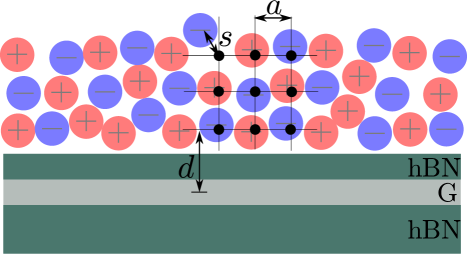
At room temperature, the Coulomb interaction between neighboring ions is much larger than , so the positions of the ions are strongly correlated. They form a structure that resembles sodium chloride, with alternating anions and cations arranged periodically with spacing . If the ions were arranged exactly periodically, they would not cause any scattering.111It might alter the band structure of the channel near . Scattering of carriers in the channel is due to small shifts, , of the ions from their periodic positions, as shown in Fig. 1. These shifts can be due to both packing disorder and thermal fluctuations. Each results in a small, randomly oriented dipole with arm . An ensemble of such random dipoles scatters electrons in graphene. We consider graphene sandwiched between two layers of hBN and study the dependence of the resistance on carrier concentration and the separation between the graphene and the ions.
The potential induced by each dipole decreases with distance as . As we derive in Methods, the scattering from such dipoles leads to the resistivity
| (1) |
where
| (2) |
Here is the resistance quantum, is the carrier density, and is the Coulomb interaction parameter, where is the Fermi velocity and is the Fermi wave vector. Choosing the value for the dielectric constant is tricky because the graphene is surrounded by both hBN and ionic liquid, and hBN is an anisotropic dielectric. In the limit where the Fermi wavelength is shorter than the bottom hBN thickness and longer than the top hBN thickness, ,Landau et al. (1984) where is the dielectric constant of the ionic liquid and is the average of the in-plane and out-of-plane dielectric constants in hBN.
We can investigate the small separation limit. When , as it is when graphene is surrounded by hBN and ionic liquid, we find that for , . Thus, the resistance does not depend on the separation for separations much smaller than the Fermi wavelength.
To clarify the origin of the and dependence in Eq. (1) at , we start from the well known expression for the contribution to the resistance from randomly distributed Coulomb scatterers. Namely, the scattering from a layer ions with concentration is , where is the carrier concentration.Hwang et al. (2007) One can modify this result for scattering from dipoles with 3D concentration . First we note that the dipole potential is times smaller than Coulomb potential, and scattering is mostly due to those nearby dipoles within a distance approximately equal to the separation between carriers, which is . Using this distance as the effective , the scattering rate for dipoles is times smaller than for the Coulomb potential. Second, instead of we use two dimensional concentration . Combining these two results we get . The full calculation in Eq. (1) agrees with this intuitive result up to the numerical factor .222Note that the electron wavelength varies in our experiment between 5 and 15 nm. It is larger than the scale of additional structuring and layering of ionic liquids within nm of interfaces, which was discovered near strongly charged surfaces.Gebbie et al. (2017); Perkin et al. (2010). This structuring does not have a large impact on our results.
I.2 Ionic liquid gated graphene
Our samples have hBN above and below the graphene. The bottom hBN flake is usually close to 40 nm thick. The top flake (or “spacer”), if present, varies in thickness from 1 to 12 layers and separates the ionic liquid from the graphene. A schematic of a typical device is shown in Fig. 2. We used two ionic liquids, both with a diethylmethyl(2-methoxyethyl)ammonium (DEME) cation. To investigate the effect of disorder in the liquid, we used a bis(trifluoromethylsulphonyl)imide (TFSI) anion that is a similar size to DEME, forming a relatively ordered liquid, and a tetrafluoroborate (BF4) anion that is smaller than DEME, forming a more disordered liquid.
The devices with hBN spacers have higher mobility than both our un-protected samples and other electrolyte-gated graphene samples in the literature. Efetov and Kim (2010); Ye et al. (2011); Browning et al. (2016) Increasing the thickness of the spacer increases the mobility, as expected.
To make a quantitative estimate of the scattering from the ionic liquid, we presume Matthiessen’s rule holds, so that the sheet resistance is
| (3) |
where arises from scattering unrelated to the ionic liquid, such as from phonons and crystal defects. We measured in all samples before adding ionic liquid and found little variation from sample to sample. We presumed that this contribution to the resistance remained unchanged after adding ionic liquid.333The scattering rate from any process that depends on the dielectric constant will change when liquid is added since the dielectric constant changes. However, phonon and short-range scattering, which are the main contributions to , are mostly independent of dielectric constant. We used Eq. (1) to find the total scattering from the ionic liquid by fitting one parameter - the average relative displacement of the ions - to the data.
In our calculations, we used an average ion diameter of Å for DEME-TFSI and 7 Å for DEME-BF4.Sato et al. (2004) We also used , where is the number of hBN layers and Å is the thickness of a single layer of hBN. For the dielectric constant, we note that the in-plane and out-of-plane dielectric constants of hBN are 4 and 7. Geick et al. (1966) The dielectric constants of several liquids similar to the two we use in our study vary between 10 and 15. Wakai et al. (2005) Taking a rough average of these values, we used .
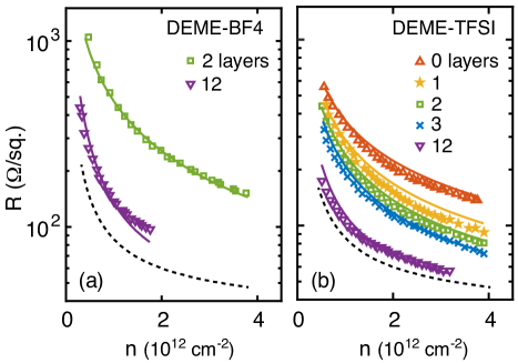
In Fig. 3, we show that the fit agrees well with the data over a range of hBN spacer thicknesses. For DEME-TFSI and DEME-BF4 ionic liquids we get and respectively. Since the size difference between DEME and BF4 is larger than between DEME and TFSI, we expect more disorder in the bulk liquid in DEME-BF4. Indeed, the observed sheet resistances for DEME-BF4 are larger than for DEME-TFSI, and the best fit value of is greater. We also note that for both liquids, consistent with the Lindemann melting criterion, which states that in a liquid the typical shift is larger than 10% of the atomic distance. Lindemann (1910)
In the derivation of Eq. (1) we assume that the dipoles are randomly oriented and are uncorrelated. Let us dwell here on the justification of this assumption. The Coulomb interaction energy between neighboring ions, , is much larger than room temperature, . Gebbie et al. (2015). On the other hand, the interaction energy between nearest-neighbor dipoles is of the order of and, for the experimental values , does not exceed . Therefore, the orientation of the dipoles can be approximately considered as random.
I.3 Scattering from excess surface ions
To change the carrier density by gating, there must be an excess of one species of ion near the hBN. These ions are reminiscent of delta-doping layers in GaAs quantum wells, which are known to cause Coulomb scattering of the carriers in the two-dimensional electron gas. Pfeiffer et al. (1989); Das Sarma et al. (2015) To isolate the effect of the excess surface ions, we used the silicon back gate to set the carrier density in the graphene to be different from the surface ion concentration in the liquid.
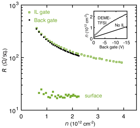
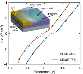
The scattering from the bulk liquid, , depends only on the carrier density. It is insensitive to whether carriers were induced by the back gate or by excess ions. However, the resistance due to the scattering from the excess ions is proportional to the excess ion concentration . It decreases when the back gate is used to induce carriers. Using the back gate to reach a certain electron density should result in less scattering than using the top gate to reach the same carrier density, since using the back gate results in lower excess ion concentration. To quantitatively estimate the scattering from excess ions, we could take the difference in resistance between carriers induced by the top gate () and back gate (). However, there is some coupling between the back gate and the ionic liquid, so changing the back gate voltage changes both the carrier density and the excess ion concentration. By measuring the capacitance between the graphene and the back gate with no ionic liquid on the sample, we can quantify this coupling. As shown in the right inset of Fig. 4, the excess ion concentration is equal to about half of the carrier density at a given back gate voltage, with the top gate grounded.
Presuming that the scattering rate from the excess ions is proportional to , the contribution of the excess ions to the graphene resistance should be , which we plot using open symbols in the Fig. 4. We see that the resistance due to excess ions at cm-2 is , an order of magnitude smaller than the expected value () if we assume that excess ions are randomly positioned near the hBN surface (at Å). Hwang et al. (2007)
There are several possible reasons why the scattering from excess ions could be suppressed below the expected value. First, the in-plane position of the ions may be correlated. In this case, the scattering from the excess ions can be suppressed, depending on the structure factor of the correlations, Li et al. (2011) analogous to correlation of ionized dopants in GaAs. Buks et al. (1994) Second, the excess ions may not be located at the surface of the hBN. If the excess ions are located away from the surface, then the scattering would be reduced. The relatively small capacitance suggests that the ions may indeed be separated from the hBN surface. As shown in Fig. 2, the geometric capacitance is about cm-2 V-1 for both liquids. Presuming that the excess ions form a simple parallel plate capacitor with the graphene, the ratio Å. Using as before, Å, which would reduce the expected contribution to scattering to approximately the observed contribution. Regardless of the mechanism, it seems that the excess surface ions contribute little to scattering.
II Conclusions
In agreement with other work, we have shown that separating the ionic liquid from the channel in an electric double layer transistor using a thin hBN spacer improves the mobility. However, we have also shown that there is always some scattering arising from the ions in the ionic liquid. A simple model that captures the disorder in the bulk liquid due to small displacements of the ions from a periodic structure can explain the observed transport properties.
A more comprehensive experiment and analysis may yield detailed information about the location of the ions in the double layer and the bulk, their correlation functions, and their behavior as a function of potential.
Already, we have seen that there is a trade-off between achieving high carrier densities, which requires thin hBN spacers, and achieving high mobilities, which requires thick spacers. With no spacer, we have shown that there is an upper limit to the mobility that can be achieved with ionic liquid gates.
III Methods
III.1 Derivation of Model Results
So long as the mean free path, , is much larger than the Fermi wavelength, the resistance per square of graphene can be rewritten in terms of the scattering time, , asAndo (2006)
| (4) |
The scattering time is Das Sarma et al. (2011)
| (5) |
Here is the perpendicular distance from the ion to the graphene, is the scattering vector, is the volume concentration of scattering centers in the ionic liquid, is the Fourier transform of the scattering potential, is the dielectric function, is the transport factor for graphene that prohibits back scattering, is the form factor for the carrier wavefunctions, and is the energy dispersion relation. In graphene, , , and .
So we find:
| (6) |
In this derivation, we have assumed that the electron gas is degenerate, which is a valid assumption for densities above cm-2 in graphene at room temperature. All measurements in our experiments were made above this density. Thus, for a given the scattering rate does not depend on temperature. At the same time, it is likely that increases with temperature and, therefore, resistivity increases with as well.
In the case of bulk disorder, each shifted ion contributes to the scattering, so . The dipole potential is , where is the displacement of the ion, and is the angle between the axis of the dipole and the position of an electron. The average distance between electrons, , is greater than the thickness of the top hBN. From an electrostatic point of view, we can neglect the top hBN and assume that the graphene is placed between the ionic liquid and the bottom hBN. The effective dielectric constant in this case is .
After averaging over all possible dipole orientations, we find
| (7) |
where is the modified Bessel function of the second kind.
III.2 Fabrication of graphene heterostructures
We fabricated hBN-graphene-hBN stacks using a dry transfer method with PPC/PDMS stamps and deposited them on highly doped silicon substrates with 300 nm of oxide. Wang et al. (2013) We used e-beam lithography (30 kV, 250 - 300 C/cm2, 1:3 isopropanol:water developer) with 950k PMMA resist, followed by reactive ion etching in a mixture of 10% O2 and 90% CHF3 to define the hall bars (Oxford PlasmaLab 80, 50 W, 150 mTorr). We e-beam evaporated 5 nm Cr and 75 nm Au to make contacts and annealed the final devices in 10% H2 in Ar at 350 C for 1 hr. We found that sweeping an AFM tip across the surface in contact mode (50 nN) after annealing further increased the mobility, and we did this treatment on all samples. After sweeping, the mobilities were close to the phonon limit. Hwang and Das Sarma (2008) We fabricated a Pt gate electrode nearby and dropped a small amount of ionic liquid (baked overnight at 80 C in high vacuum) over the gate and the hall bar.
III.3 Transport measurements
All measurements were performed at 300 K in high vacuum ( Torr). We used a Stanford Research Systems SR830 lockin amplifier to measure 4-terminal resistance and Hall voltage. The current sourced was 1 A, and the Hall bars were 2 m by 3 m. We calculated carrier density from the difference in the Hall voltage at 20 mT and 20 mT, which was applied using a solenoid wound around the vacuum chamber. We used a Keithley K2400 Sourcemeter to apply gate voltages. The leakage currents were less than 1 A/cm2.
We measured the applied potential relative to a Fc/Fc+ reference electrode. We dissolved a small amount of ferrocene (Fc) and ferrocenium (Fc+) directly in the ionic liquid ( mg/mL) and measured the potential on an immersed Pt wire using a high impedance ( 10G) voltmeter. At a given gate voltage, the potential at the Fc/Fc+ reference is about 300 mV less than the potential at a Ag/Ag+ reference in 1 M AgNO3, which was formed by dissolving AgNO3 in ionic liquid in a separate tube that was separated by 5 m diameter fritted glass from the rest of the cell.
IV Acknowledgement
We thank Shu Hu and Nathan Lewis for providing valuable insight and lab assistance to develop the reference electrode used in this work. The experimental work was supported by the Department of Energy, Laboratory Directed Research and Development funding, under contract DE-AC02-76SF00515. The theoretical work was supported by the National Science Foundation through the University of Minnesota MRSEC under Award Number DMR-1420013. Part of this work was performed at the Stanford Nano Shared Facilities, supported by the National Science Foundation under award ECCS-1542152. T. P. was supported by the Department of Defense through a National Defense Science and Engineering Graduate Fellowship and by a William R. and Sara Hart Kimball Stanford Graduate Fellowship. K.V.R was supported by the Russian Science Foundation under grant 17-72-10072. K.W. and T.T. acknowledge support from the Elemental Strategy Initiative conducted by the MEXT, Japan and JSPS KAKENHI Grant Numbers JP15K21722.
References
- Goldman (2014) Goldman, A. M. Electrostatic Gating of Ultrathin Films. Annu. Rev. Mater. Res. 2014, 44, 45–63.
- Ueno et al. (2008) Ueno, K.; Nakamura, S.; Shimotani, H.; Ohtomo, A.; Kimura, N.; Nojima, T.; Aoki, H.; Iwasa, Y.; Kawasaki, M. Electric-Field-Induced Superconductivity in an Insulator. Nat. Mater. 2008, 7, 855–858.
- Scherwitzl et al. (2010) Scherwitzl, R.; Zubko, P.; Lezama, I. G.; Ono, S.; Morpurgo, A. F.; Catalan, G.; Triscone, J.-M. Electric-Field Control of the Metal-Insulator Transition in Ultrathin NdNiO3 Films. Adv. Mater. 2010, 22, 5517–5520.
- Nakano et al. (2012) Nakano, M.; Shibuya, K.; Okuyama, D.; Hatano, T.; Ono, S.; Kawasaki, M.; Iwasa, Y.; Tokura, Y. Collective Bulk Carrier Delocalization Driven by Electrostatic Surface Charge Accumulation. Nature 2012, 487, 459–462.
- Jeong et al. (2013) Jeong, J.; Aetukuri, N.; Graf, T.; Schladt, T. D.; Samant, M. G.; Parkin, S. S. P. Suppression of Metal-Insulator Transition in VO2 by Electric Field-Induced Oxygen Vacancy Formation. Science 2013, 339, 1402–1405.
- Shimizu et al. (2013) Shimizu, S.; Takahashi, K. S.; Hatano, T.; Kawasaki, M.; Tokura, Y.; Iwasa, Y. Electrically Tunable Anomalous Hall Effect in Pt Thin Films. Phys. Rev. Lett. 2013, 111, 216803.
- Petach et al. (2014) Petach, T. A.; Lee, M.; Davis, R. C.; Mehta, A.; Goldhaber-Gordon, D. Mechanism for the Large Conductance Modulation in Electrolyte-Gated Thin Gold Films. Phys. Rev. B 2014, 90, 081108(R).
- Bubel et al. (2015) Bubel, S.; Hauser, A. J.; Glaudell, A. M.; Mates, T. E.; Stemmer, S.; Chabinyc, M. L. The Electrochemical Impact on Electrostatic Modulation of the Metal-Insulator Transition in Nickelates. Appl. Phys. Lett. 2015, 106, 122102.
- Browning et al. (2016) Browning, A.; Kumada, N.; Sekine, Y.; Irie, H.; Muraki, K.; Yamamoto, H. Evaluation of Disorder Introduced by Electrolyte Gating Through Transport Measurements in Graphene. Appl. Phys. Express 2016, 065102.
- Gallagher et al. (2015) Gallagher, P.; Lee, M.; Petach, T. A.; Stanwyck, S. W.; Williams, J. R.; Watanabe, K.; Taniguchi, T.; Goldhaber-Gordon, D. A High-Mobility Electronic System at an Electrolyte-Gated Oxide Surface. Nat. Commun. 2015, 6, 6437.
- Li et al. (2015) Li, L. J.; O’Farrell, E. C. T.; Loh, K. P.; Eda, G.; Özyilmaz, B.; Castro Neto, A. H. Controlling Many-Body States by the Electric-Field Effect in a Two-Dimensional Material. Nature 2015, 529, 185–189.
- Sato et al. (2004) Sato, T.; Masuda, G.; Takagi, K. Electrochemical Properties of Novel Ionic Liquids for Electric Double Layer Capacitor Applications. Electrochim. Acta 2004, 49, 3603–3611.
- Novoselov et al. (2005) Novoselov, K. S.; Geim, A. K.; Morozov, S. V.; Jiang, D.; Katsnelson, M. I.; Grigorieva, I. V.; Dubonos, S. V.; Firsov, A. A. Two-Dimensional Gas of Massless Dirac Dermions in Graphene. Nature 2005, 438, 197–200.
- Dean et al. (2010) Dean, C. R.; Young, A. F.; Meric, I.; Lee, C.; Wang, L.; Sorgenfrei, S.; Watanabe, K.; Taniguchi, T.; Kim, P.; Shepard, K. L.; Hone, J. Boron Nitride Substrates for High-Quality Graphene Electronics. Nat. Nanotechnol. 2010, 5, 722–726.
- Hwang et al. (2007) Hwang, E. H.; Adam, S.; Sarma, S. D. Carrier Transport in Two-Dimensional Graphene layers. Phys. Rev. Lett. 2007, 98, 2–5.
- Chen et al. (2008) Chen, J.-H.; Jang, C.; Xiao, S.; Ishigami, M.; Fuhrer, M. S. Intrinsic and Extrinsic Performance Limits of Graphene Devices on SiO2. Nat. Nanotechnol. 2008, 3, 206–209.
- Landau et al. (1984) Landau, L. D.; Bell, J. S.; Kearsley, M. J.; Pitaevskii, L. P.; Lifshitz, E. M.; Sykes, J. B. Electrodynamics of Continuous Media; 1984; Vol. 8; p 37.
- Gebbie et al. (2017) Gebbie, M. A.; Smith, A. M.; Dobbs, H. A.; Lee, A. A.; Warr, G. G.; Banquy, X.; Valtiner, M.; Rutland, M. W.; Israelachvili, J. N.; Perkin, S.; Atkin, R. Long Range Electrostatic Forces in Ionic Liquids. Chem. Commun. 2017, 53, 1214–1224.
- Perkin et al. (2010) Perkin, S.; Albrecht, T.; Klein, J. Layering and Shear Properties of an Ionic Liquid, 1-Ethyl-3-Methylimidazolium Ethylsulfate, Confined to Nano-Films Between Mica Surfaces. Phys. Chem. Chem. Phys. 2010, 12, 1243–1247.
- Fang et al. (2007) Fang, T.; Konar, A.; Xing, H.; Jena, D. Carrier Statistics and Quantum Capacitance of Graphene Sheets and Ribbons. Appl. Phys. Lett. 2007, 91, 092109.
- Efetov and Kim (2010) Efetov, D. K.; Kim, P. Controlling Electron-Phonon Interactions in Graphene at Ultrahigh Carrier Densities. Phys. Rev. Lett. 2010, 105, 256805.
- Ye et al. (2011) Ye, J.; Craciun, M. F.; Koshino, M.; Russo, S.; Inoue, S.; Yuan, H.; Shimotani, H.; Morpurgo, A. F.; Iwasa, Y. Accessing the Transport Properties of Graphene and Its Multilayers at High Carrier Density. Proc. Natl. Acad. Sci. U.S.A. 2011, 108, 13002–13006.
- Geick et al. (1966) Geick, R.; Perry, C. H.; Rupprecht, G. Normal Modes in Hexagonal Boron Nitride. Phys. Rev. 1966, 146, 543–547.
- Wakai et al. (2005) Wakai, C.; Oleinikova, A.; Ott, M.; Weingärtner, H. How Polar are Ionic Liquids? Determination of the Static Dielectric Constant of an Imidazolium-Based Ionic liquid by Microwave Dielectric Spectroscopy. J. Phys. Chem. B 2005, 109, 17028–17030.
- Lindemann (1910) Lindemann, F. A. The Calculation of Molecular Vibration Frequencies. Physik. Z 1910, 11, 609–612.
- Gebbie et al. (2015) Gebbie, M. A.; Dobbs, H. A.; Valtiner, M.; Israelachvili, J. N. Long-Range Electrostatic Screening in Ionic Liquids. Proc. Natl. Acad. Sci. U.S.A. 2015, 112, 7432–7437.
- Pfeiffer et al. (1989) Pfeiffer, L.; West, K. W.; Stormer, H. L.; Baldwin, K. W. Electron Mobilities Exceeding cm2/V s in Modulation-Doped GaAs. Appl. Phys. Lett. 1989, 55, 1888–1890.
- Das Sarma et al. (2015) Das Sarma, S.; Hwang, E. H.; Kodiyalam, S.; Pfeiffer, L. N.; West, K. W. Transport in Two-Dimensional Modulation-Doped Semiconductor Structures. Phys. Rev. B 2015, 91, 205304.
- Li et al. (2011) Li, Q.; Hwang, E. H.; Rossi, E.; Das Sarma, S. Theory of 2D Transport in Graphene for Correlated Disorder. Phys. Rev. Lett. 2011, 107, 156601.
- Buks et al. (1994) Buks, E.; Heiblum, M.; Shtrikman, H. Correlated Charged Donors and Strong Mobility Enhancement in a Two-Dimensional Electron Gas. Phys. Rev. B 1994, 49, 14790–14793.
- Ando (2006) Ando, T. Screening Effect and Impurity Scattering in Monolayer Graphene. J. Phys. Soc. Jpn. 2006, 75, 1–7.
- Das Sarma et al. (2011) Das Sarma, S.; Adam, S.; Rossi, E. Electronic Transport in Two-Dimensional Graphene. Rev. Mod. Phys. 2011, 83, 407.
- Wang et al. (2013) Wang, L.; Meric, I.; Huang, P. Y.; Gao, Q.; Gao, Y.; Tran, H.; Taniguchi, T.; Watanabe, K.; Campos, L. M.; Muller, D. A.; Guo, J.; Kim, P.; Hone, J.; Shepard, K. L.; Dean, C. R. One-Dimensional Electrical Contact to a Two-Dimensional Material. Science 2013, 342, 614–617.
- Hwang and Das Sarma (2008) Hwang, E. H.; Das Sarma, S. Acoustic Phonon Scattering Limited Carrier Mobility in Two-Dimensional Extrinsic Graphene. Phys. Rev. B 2008, 77, 115449.