Coherent control of single electrons: a review of current progress
pacs:
03.65.-w, 73.21.La, 73.22.f; check !!!Abstract
In this report we review the present state of the art of the control of propagating quantum states at the single-electron level and its potential application to quantum information processing. We give an overview of the different approaches which have been developed over the last ten years in order to gain full control over a propagating single electron in a solid state system. After a brief introduction of the basic concepts, we present experiments on flying qubit circuits for ensemble of electrons measured in the low frequency (DC) limit. We then present the basic ingredients necessary to realise such experiments at the single-electron level. This includes a review of the various single electron sources which are compatible with integrated single electron circuits. This is followed by a review of recent key experiments on electron quantum optics with single electrons. Finally we will present recent developments about the new physics that emerges using ultrashort voltage pulses. We conclude our review with an outlook and future challenges in the field.
I Introduction:
In current semiconductor technology, where the integrated circuits are composed of transistors, which are nowadays as small as a few tens of nanometers in scale, the electronic circuits are still operated with of a huge number of electrons. The ultimate goal, in this respect, is the realisation of integrated circuits at the single-electron level. Over the past decade, an important effort has been made in the field of low-dimensional electronic conductors towards single electron electronics with the goal to gain full control over single electrons in solid state devices. Nowadays it is possible to confine and manipulate single electrons in a very controlled way in semiconductor nanostructures such as nanowires or quantum dots Kouwenhoven et al. (1997); van der Wiel et al. (2002); Fujisawa et al. (2006); De Franceschi et al. (2010); Laird et al. (2015). However, in order for the single electron circuits of the future to lead to useful applications, one requires a mechanism to transport and interconnect a single electron from one functional part of the circuit to another and to manipulate it in a very controlled way. In addition, the ability to control single electrons on-demand enables electron quantum optics experiments where single electrons emitted in a ballistic electronic interferometer play the role of single photons emitted in an optical medium in quantum optics.
Coherent manipulation of single electrons in solid state devices are also attractive for quantum information purposes because they have a high potential for scalability. Depending on the system used, the charge or the spin may code binary qubit information. A particular appealing idea is to use a single flying electron itself as the conveyor of quantum information Bertoni et al. (2000); Ionicioiu et al. (2001a); Barnes et al. (2000); Beenakker et al. (2004); Bertrand et al. (2016a). Such electronic flying qubits allow performing quantum operations on qubits while they are being coherently transferred. Information processing typically takes place in the nodes of the quantum network on locally controlled qubits, but quantum networking would require flying qubits to exchange information from one location to another DiVincenzo (2000). It is therefore of prime interest to develop ways of transferring information from one node to the other. The availability of flying qubits would enable the possibility to develop new non-local architectures for quantum computing with possibly cheaper hardware overhead than e.g. surface codes Fowler et al. (2012).
Photons in vacuum are a natural choice for flying qubits due to their long coherence time. Solid state electronic devices have advantage in terms of size and hence for possible scalability, however, with a serious drawback of a much shorter coherence time. Electronic spin states are often chosen as spatially localised qubits as they can be easily confined to a small volume van der Wiel et al. (2002); Hanson et al. (2007); Zwanenburg et al. (2013); Awschalom et al. (2013). Coherent transport of quantum information has been demonstrated in solid state systems by transporting single electrons in multiple quantum dot networks Flentje et al. (2017); Fujita et al. (2017) or by coupling of superconducting qubits to microwave photons Wallraff et al. (2004); Houck et al. (2007); Roch et al. (2014). Recent advances in the field of electron quantum transport have shown that solid-state flying qubits based on single electrons are also very promising as these systems have possible applications in electron interferometry and entanglement.
In this review we concentrate on integrated electronic circuits operated at the single-electron level in semiconductor heterostructures and outline their potential towards a flying qubit architecture. We will focus in particular on quantum experiments appropriate for electron quantum optics where the emitted single electrons play the role of flying charge qubits. We give a comprehensive review of the present state of the art and put emphasis on the connection to quantum information processing and the physical phenomena underlying realistic devices.
II Basic theoretical concepts for flying qubit architectures with single electrons
The flying qubits that will be discussed in this review aim to encode the quantum information into two different paths (or rails) that can be taken by an electron during its propagation. Such a quantum rail can be defined by a one-dimensional channel along which a single-electron wave packet is propagating ballistically. This can be experimentally realised in a gate-defined nanostructure on top of a two-dimensional electron gas formed at the interface of a semiconductor heterostructure and will be described in detail in section III. In order to realise this flying qubit architecture with single flying electrons, it is necessary to be able to control the state of an electron via two independent qubit rotations.
II.0.1 Single-qubit operations
Let us define the two qubit states and on the Bloch sphere as shown in figure 1. A rotation around the x-axis with rotation angle is described by the following rotation matrix:
| (1) |
while a rotation around the z-axis with rotation angle is given by :
| (2) |
Such rotation matrices can also be expressed in terms of Pauli matrices: , . They are usually referred to as single qubit rotations Nielsen and Chuang (2000). In order to construct any arbitrary state on the Bloch sphere, it is enough to combine two of the three possible rotation matrices. Combining the two rotation matrices, it is also possible to construct a universal transformation Barenco et al. (1995); Bertoni et al. (2000)
| (3) |
Such a scheme can be implemented into a coherent nanoelectronic circuit by coupling two quantum rails Ionicioiu et al. (2001a) as schematised in figure 1(a).
One can define two qubit states and by the presence of the electron in the lowest energy state of one of the two rails:
= electron present in the upper rail
= electron present in the lower rail
When the confinement potential of the two quantum wires are identical in the region, where the two quantum wires are coupled by a tunnel barrier (interaction region), hybridisation between these two states occurs and the new eigenbasis is given by the symmetric and antisymmetric state del Alamo and Eugster (1990); Tsukada et al. (1990); Xu et al. (1993) :
| (4) |
By injecting an electron into the upper rail , the wave function will evolve into a superposition of ( + ). While travelling through the interaction region of length , the wave function of the electron will then pick up a phase and will evolve into (), with () being the wave vector of the symmetric (antisymmetric) state. Projecting back the wave function onto the two output channels allows obtaining the probability of finding an electron in the upper (lower) channel. Doing the same calculation by injecting an electron in state (lower rail) one can then work out the complete transmission matrix which reads:
| (5) |
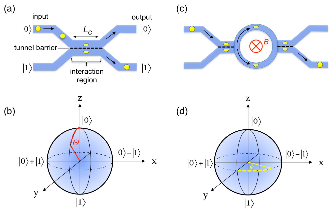
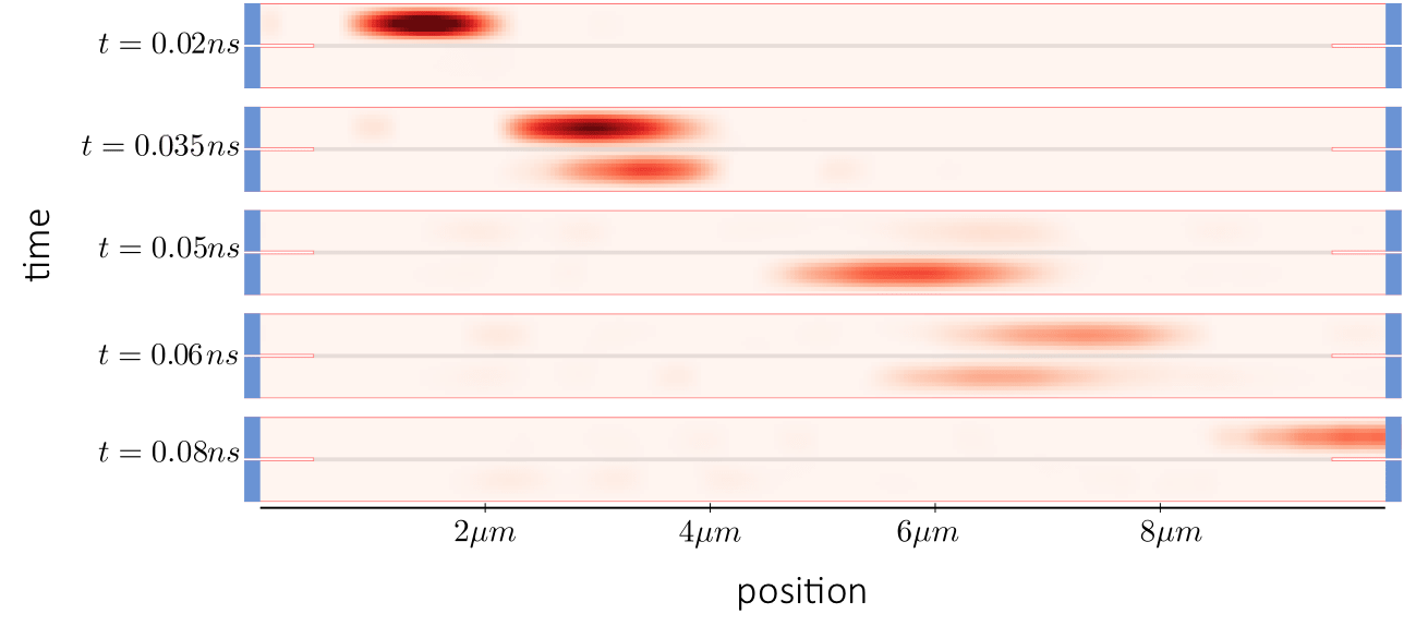
By comparing this to equation (1) one can immediately see that this matrix corresponds to a rotation matrix with rotation angle . This means that the electron wave packet propagating through the tunnel-coupled wire will oscillate between states and (upper and lower wire) and hence represents a rotation around the x-axis of the Bloch sphereBautze et al. (2014). Time resolved numerical simulations of the propagation of a single-electron wave packet through such tunnel-coupled wires for realistic experimental conditions can now be realised Bertoni et al. (2000); Gaury et al. (2014); Bautze et al. (2014). An example of such real-time simulations is shown in figure 2.
As mentioned above, to attain any arbitrary final state on the Bloch sphere, another rotation has to be implemented. This can be done by connecting the wire to a ring geometry in order to pick up an additional phase due to the Aharonov-Bohm effect Aharonov and Bohm (1959); Tonomura and Batelaan (2009) as schematised in Fig. 1(c). Electron interference arises due to a phase difference between electrons passing through the upper or lower path. The phase difference is given by , where is the wave vector, the path along the ring, the magnetic field and the surface area enclosed by the ring structure. One way of changing is to simply change the Aharonov-Bohm flux. From an experimental point of view, this is however not very practical as the magnetic field cannot be changed on fast timescales. For an electron travelling at the Fermi velocity of approximately 1 m/s passing through a 10 m long coherent quantum conductor will only take 100 ps. A more practical way is to modify the phase by changing the wave vector . This can be done on a very fast time scale using an electrostatic gate. Such a modification of by an electrostatic gate will be described in section III.2. Combining both single qubit rotations, the tunnel-coupled wire as well as the Aharonov-Bohm ring, one can then entirely control the phase of the electron and realise a flying qubit architecture Yamamoto et al. (2012).
II.0.2 Two-qubit operations
The next step is to combine the single qubit operations in order to perform a two-qubit operation Ionicioiu et al. (2001a). It is actually possible to use the interaction region to control the state of one qubit with a second qubit and to realise for instance a controlled phase gate. This quantum gate exploits the Coulomb interaction between two single electrons in two different pairs of coupled quantum wires. So far we have only considered one electron at a time in the interaction region. It is however possible to control the phase of an electron in one of the two rails by the presence of another electron in the other rail due to Coulomb interaction. This scheme is usually termed a Coulomb coupler (CC) and allows controlling the phase of the target qubit using a second control qubit. A possible design for the realisation of a controlled phase gate for flying electrons using a CC is shown in figure 3. Two qubits (A and B) are coupled in the center by a CC. In addition four tunnel-coupled wires are added, which allow for tunnelling between the wires and hence controlling the rotation angle of each individual qubit. When set at , they act as beam splitters. Other schemes have been proposed to implement two qubit gates such as ballistic Aharonov-Bohm qubits Yu and Voskoboynikov (2008); Schomerus and Robinson (2007) or surface acoustic wave driven electrons Barnes et al. (2000). Here we concentrate on the most general case which can be applied to both systems.
The induced phase on each electron in the CC is proportional to the coupling strength (capacitive coupling) between the two rails and the interaction time . In order to have a strong coupling between the two electrons in the interaction region, the two qubit rails have to be sufficiently close. On the other hand, tunnelling between the two rails should be suppressed. A CC should therefore have a large potential barrier in order to prevent electron tunnelling from one rail to the other, and at the same time the two rails should be close enough to induce a significant phase shift. For the experimental systems we will describe in the following, this can be achieved by adjusting the barrier height induced by the electrostatic gate of the CC which separates the two rails as well as the length of the interaction region.
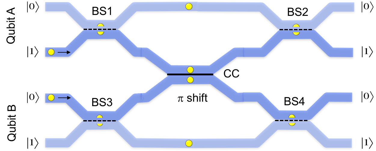
The operation of the CC in figure 3 can hence be written as:
,
where .
This phase shift can be measured experimentally by performing an interference experiment and observe a change in the detection probability of an electron in one of the output ports.
To do that, the rotation angle for BS1 and BS2 is set to , the one for BS3 and BS4 is set to .
In this case the probability of detecting an electron in oscillates as one changes the barrier height of the CC, which modulates .
The inverted oscillation should be observed in the other output.
For the same circuit a controlled phase gate can be implemented by setting to , the rotation angle for BS1 and BS2 to , the one for BS3 to , and the one for BS4 to .
This device structure also allows to entangle two different qubits Buscemi et al. (2012). To do so one can for instance activate the beam splitters ( for all BS) and adjust the Coulomb coupler in such a way that a phase shift is induced between the two propagating electrons. By sending synchronously one electron into input A1 and B0 the outcome of such a scheme is a maximally entangled Bell state Ionicioiu et al. (2001b) , where and . Another interesting feature of this system is that it is easily scalable by simply adding several qubits in parallel to realise a multi qubit system. Combination of an arbitrary single qubit rotation ( in Eq. 3) and a controlled phase gate allows then to perform an arbitrary unitary operation for a n-qubit system Nielsen and Chuang (2000). A similar approach to scale up the system is also used in linear quantum optics Knill et al. (2001); O’Brien et al. (2003); Politi et al. (2008); Carolan et al. (2015).
The experimental realisation of such a system is by all means not trivial. Several important requirements have to be fulfilled such as high fidelity on-demand single electron injection as well as single-shot read-out of the electrons at the output ports. Another important requirement is that the electrons within the different quantum rails have to be synchronised at all times in order to properly perform two-qubit gating, as the two electrons have to reach simultaneously the Coulomb coupling window. All these issues will be addressed in detail in sections III-VI by giving an overview of the different approaches developed in the field to gain full control of electron transport at the single-electron level.
III Low-frequency transport in quantum coherent circuits
We have seen in section II that beam splitters, phase shifters and interferometers are the basic elements needed to realise electronic flying qubits. The most promising experimental systems to realise such electronic flying qubits are at present two-dimensional electron systems formed at the interface of a GaAs/AlGaAs heterostructure. These systems are extremely well mastered and electron trajectories can be easily implemented by engineering the desired quantum rails using electrostatic gates deposited on the surface of the GaAs heterostructure. The phase coherence length in such systems can attain several tens of micrometers at low temperatures ( mK) Roulleau et al. (2008a); Niimi et al. (2009, 2010), which is sufficient to implement many gate operations on the fly.
The control and manipulation of the phase of an electron is of prime importance for the realisation of flying qubits at the single-electron level. In order to access the phase of an electron it is usually convenient to realise a two-path interference experiment with electronsJönsson (1961); Tonomura et al. (1989); Tonomura and Batelaan (2009), similar to the well known Young’s double slit experiment for photons Young (1804); Hecht (1974). A simple realisation is an Aharonov-Bohm ring of micrometer size, such that phase coherence of the electrons is ensured throughout the entire device Webb et al. (1985); Chandrasekhar et al. (1985); Washburn and Webb (1986); Yacoby et al. (1995); Buks et al. (1998); Gustavsson et al. (2008) when working at low temperatures. At the entrance of the ring structure the electron wave function is split into two paths and recombined at the output as depicted in figure 1c. A phase difference is induced between the upper and lower arm of the ring by means of an externally applied magnetic field 111more precisely, the electron couples to the vector potential Aharonov and Bohm (1959) rather than the magnetic field, hence even if the electron does not experience a magnetic field, for instance when passing next to an infinite solenoidal coil, the electron picks up a phase (see also ref. Tonomura and Batelaan (2009)). When scanning the magnetic field, the conductance oscillates as a function of magnetic field with a period which is proportional to the surface area enclosed by the two trajectories. As will be detailed below, the realisation of a true two-path interferometer is quite challenging as electrons in solids behave quite differently than photons in vacuum. Contrary to photons, electrons in solids can backscatter and this complicates seriously the interpretation of the interference pattern Büttiker et al. (1985); Yeyati and Büttiker (1995); Yacoby et al. (1996).
One possibility to overcome these unwanted effects is to work in the quantum Hall regime, where transport is realised along edge states. This system is particularly appealing as backscattering is suppressed due to the chirality of the system. It is for instance possible to realise the electronic analogue of the optical Mach –Zehnder interferometer (MZI). A beam splitter, made from a quantum point contact (QPC) van Wees et al. (1988); Wharam et al. (1988) splits an incoming electron beam into two independent beams which are guided towards a second beam splitter where they recombine and interfere Ji et al. (2003); Roulleau et al. (2008a); Litvin et al. (2008) as schematised in figure 4. In the past, this system has been used to study fundamental phenomena such as quantum coherence Huynh et al. (2012), entanglement Neder et al. (2007a), electron-electron interactions as well as two-particle interference Neder et al. (2007b).
Another possibility to realise a Mach–Zehnder (MZ) type interferometer is by combining an Aharonov-Bohm ring to two tunnel-coupled wires Yamamoto et al. (2012). In this case (see figures 8 and 9 ) the tunnel-coupled wires Debray et al. (2001); Yamamoto et al. (2006); Laroche et al. (2014) fulfill the function of the beam splitters as we have already seen in section II. This system can be operated as a flying qubit MZ interferometer by simply controlling the phase of the electrons via electrostatic gates Bautze et al. (2014) at basically zero magnetic field.
Since Mach–Zehnder interferometry represents an essential ingredient for the realisation of electronic flying qubits, we review these two different Mach–Zehnder interferometers in more detail in the next two sections. Let us emphasise that these experiments were done in the DC limit by applying a voltage at low frequencies and billions of coherent electrons are passing through the nano-device. Experiments at the single-electron level with such interferometers are quite challenging and have not yet been realised. We will come back to this issue in sections IV – VI
III.1 Mach–Zehnder interferometry in the quantum Hall regime
In this section, we discuss the different type of electronic interferometers which have been studied in the quantum Hall regime. In GaAs/AlGaAs, several questions have been addressed to improve our understanding of electronic interferometry and electron entanglement. An edge state in the quantum Hall regime, together with the electronic beam splitter, is a building block of electronic interferometry. Historically, one of the first addressed questions was to unveil the coherence properties of the edge states in the quantum Hall regime. This has been realized using a MZI Ji et al. (2003); Neder et al. (2006); Roulleau et al. (2007, 2008a); Litvin et al. (2008). Another big challenge was to use MZIs to make basic quantum operations. The combination of the two MZIs lead to the two-electron Aharonov-Bohm interferometer and should allow for generation of entangled states Samuelsson et al. (2004); Neder et al. (2007b), assuming an appropriate tuning of the electronic beam splitters.
III.1.1 The electronic Mach–Zehnder interferometer
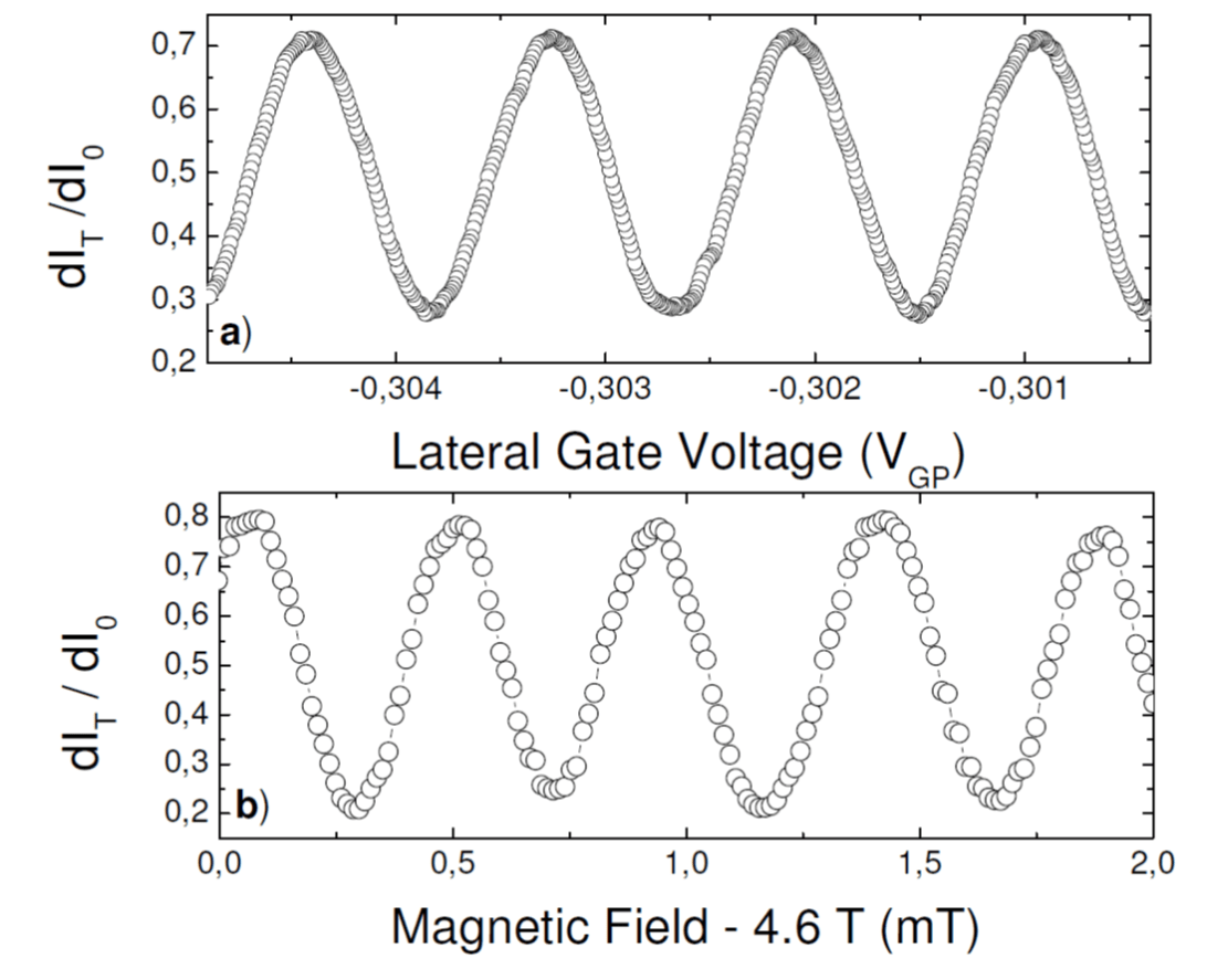
The electronic MZI is the electronic counterpart of the optical one Ji et al. (2003), QPCs working as electronic beam splitters and ohmic contacts as detectors. A first QPC splits the incoming edge current to an upper path (u) and a down path (d) (see Fig. 4). The two electronic trajectories will follow the edge of the sample designed to ensure a zero length difference between the upper (u) and down (d) trajectories. The two electronic trajectories recombine then on a second QPC. This leads to interference which is visible in the measured transmitted current I, while the reflected part of the current is collected in a grounded inner tiny ohmic contact. This is an important point in order to avoid electrons from being re-injected into the interferometer that would lead to a more complicated interference pattern. The transmission probability T through the MZI is, T = + + cos() where with the area of the interferometer, () and () the transmission and reflection probability of the first (second) beam splitter. Consequently to observe oscillations, one varies the Aharonov-Bohm (AB) flux through the surface defined by the two arms of the interferometer, either by varying the area defined by the paths (u) and (d) using a lateral gate or by sweeping the magnetic field. We have represented in Fig.5 the two different ways to reveal oscillations. One can notice that sweeping the magnetic field to reveal quantum interferences leads to a more noisy sinusoidal curve than by sweeping the lateral gate voltage
In the physics of quantum conductors, one of the fundamental length scales which sets an upper limit to the manifestation of quantum effects, is the quantum coherence length Lφ. It is the typical length over which an electron exchanges information with other degrees of freedom and looses its phase coherence. In the Integer Quantum Hall Regime, because of the chirality that prevent energy exchange processes, we expect a very long coherence length. To determine the coherence length, one has to measure the dependence of the visibility with different parameters (the bias, the temperature, the size of the interferometer).
First studies focused on the effect of a DC voltage applied on the source contact. Unexpectedly, the bias dependence of the visibility revealed an unusual lobe structure (at filling factor =1 and 2) Roulleau et al. (2007); Neder et al. (2006). This is now understood as a signature of strong Coulomb interaction between edge states and results in a separation of the spectrum of edge excitations into a slow and fast mode Levkivskyi and Sukhorukov (2008). The interaction between the two co-propagating edge states has been widely considered both theoretically and experimentally to explain coherence properties of edge states at filling factor =2 Roulleau et al. (2008b); Bocquillon et al. (2013a); Levkivskyi and Sukhorukov (2008); Lee and Eric Yang (1997); Sukhorukov and Cheianov (2007); Levkivskyi and Sukhorukov (2008); Berg et al. (2009); Levkivskyi and Sukhorukov (2012). Because of Coulomb interaction between the two edge states of opposite spins, new eigenmodes with different velocities arise: a fast mode that carries the charge and a slow neutral charge mode. A direct observation of this separation has been realised at filling factor =2 where each mode can be addressed individually Bocquillon et al. (2013b); Inoue et al. (2014); Kamata et al. (2014); Freulon et al. (2015); Hashisaka et al. (2017).
The systematic study based on the temperature and size dependence of the visibility came slightly later. It enabled to extract the coherence length Lφ at filling factor =2 (B 4.6 T), where two edge states are propagating into the interferometer (Roulleau et al., 2008a). Two conditions are necessary to measure the absolute value of Lφ. First one needs to prove its existence by varying the size on which interferences occur. Secondly, one needs to show that the interferences have a phase which does not depend on the energy of the quasiparticles (to exclude thermal smearing). This can be ensured by the geometry of the interferometer: for equal length of interferometer arms, the phase is energy independent. From the temperature dependence of the visibility , it has been shown that with T the electronic temperature and the drift velocity of the electrons. From the size dependence of the visibility Lφ 20m has been extracted at T=20mKRoulleau et al. (2008a). With some record visibilities equal to 90 Neder et al. (2007b), the MZI appears as a promising brick for more complicated geometries.
III.1.2 The two-electron Mach–Zehnder interferometer
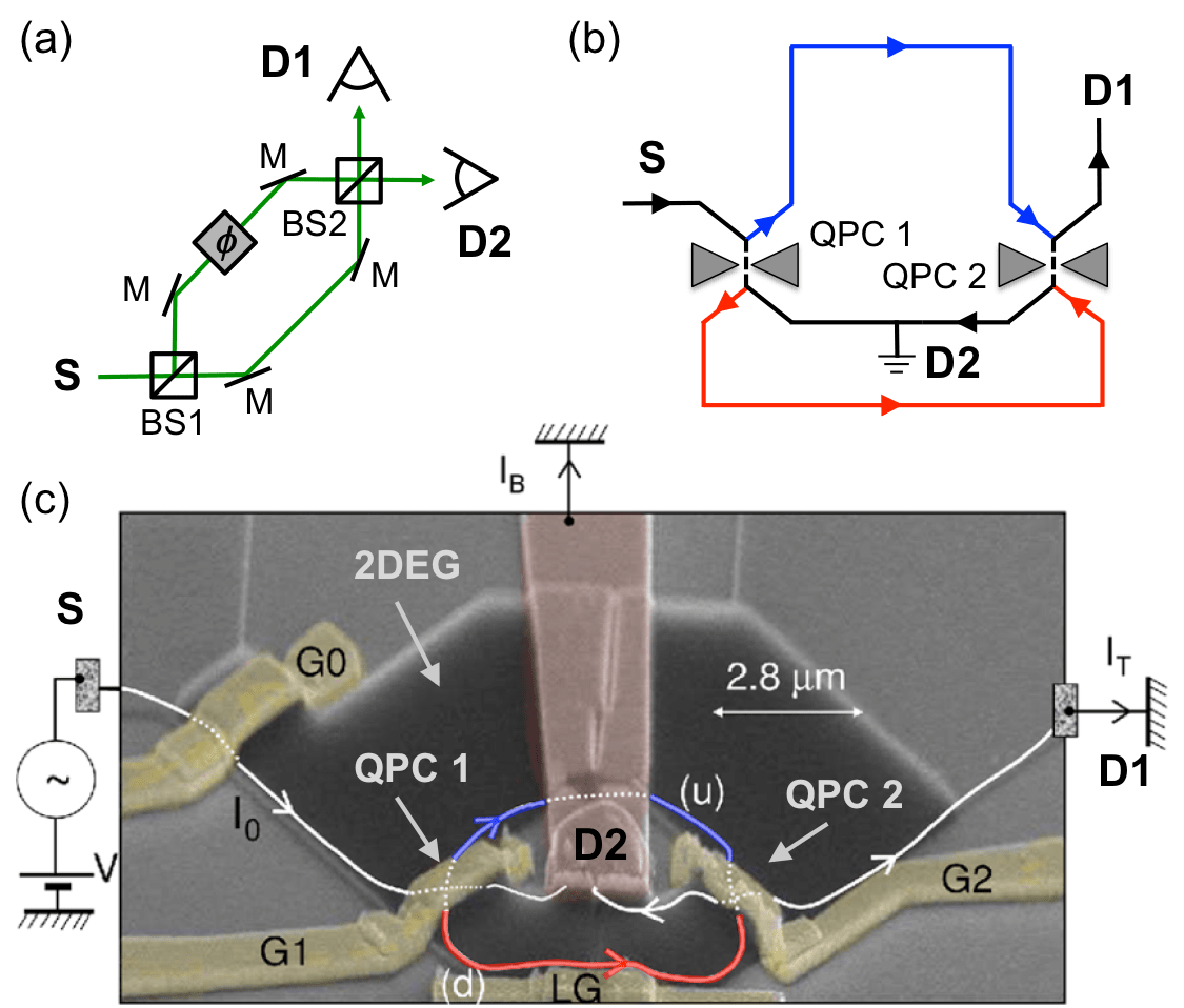
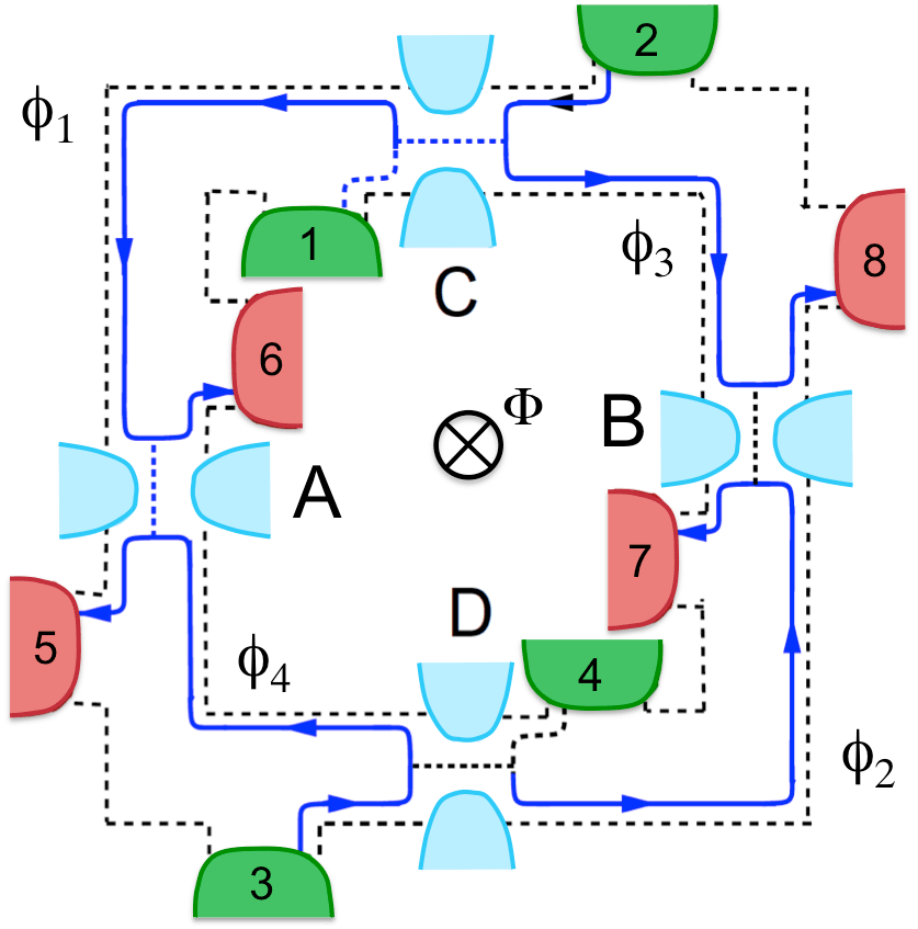
To realise quantum gates, entangled states must be generated. To create an entangled state, a two-electron interferometer where indistinguishable electrons are injected from two independent sources is necessary Samuelsson et al. (2003); Samuelsson and Büttiker (2005); Beenakker et al. (2005). As depicted in Fig. 6, electrons are injected from two independent sources 2 and 3. A, B, C and D are QPCs. Contacts 6 and 7 are grounded (contacts 1 and 4 are not used). The measurement is realised between contacts 5 and 8. The direction propagation is fixed by the magnetic field: electrons from source 2 (3) are partitioned by QPC C (D). Reflected electrons from 2 are sent to QPC B. Transmitted electrons from 3 are also sent to QPC B: at the output of QPC B it is not possible to distinguish electrons coming from 2 to those from 3. This indiscernibility is the building block of the two-electron Aharonov-Bohm effect and the orbital entanglement. The quantity that will post-select the entangled part of the output state at contacts 5 and 8 is the zero-frequency current cross correlator noted . When the gate transmissions are equal to 1/2, one can show that Samuelsson et al. (2004, 2009): where is the phase accumulated between QPCs C and A, between QPCs D and B, between QPCs C and B, between QPCs D and A (see figure 6). We now assume that a magnetic flux can be added through the sample. Due to the chirality of the electronic trajectories, one obtains a positive contribution of the magnetic flux for the phases and , and a negative one for the phases and . The global contribution related to the magnetic flux is thus equal to where is the magnetic flux across the area enclosed by the four trajectories. Varying the magnetic flux through the double MZI, one should observe oscillations of . Since none of the electrons injected from 2 (or 3) can make a complete loop around , this effect is necessarily a two-electron Aharonov-Bohm effet.
The first and so far only realisation of this experiment has been done by the Weizmann team Neder et al. (2007b). As depicted in Fig. 7(a), the experimental double MZI was composed of two single MZIs separated by a central top gate. The central gate being closed, each single MZI was independently tuned reaching a maximum visibility of 90 . The central gate is then fully opened to finally obtain the double MZI configuration. In Fig. 7(b), the cross-correlation shot noise has been measured as a function of a lateral gate voltage (varying the area defined by the four paths) or the magnetic field (exploiting the gradual decay of the magnetic field in persistent mode). Oscillations with a period compatible with two-electron interference have been observed, but only with a 25 visibility, much smaller than expected with two MZI showing 90 visibility in single electron interference. Before going further, like performing Bell’s inequalities violationBell (1966); Neder et al. (2007b); Samuelsson et al. (2003), one definitively needs to understand the mechanisms leading to this unexpected low visibility of the two-electron quantum interference.
III.2 Mach–Zehnder interferometry at low magnetic fields (AB ring with tunnel-coupled wires)
Another way to realise a MZI which works at low magnetic fields (mT ) is to combine an Aharonov-Bohm interferometer with tunnel-coupled wires. In this case the chirality is not relevant for the electron transport. As briefly mentioned before, realisation of a two-path interferometer is a direct way to realise a flying qubit. For a two-path interferometer the two qubit states and are defined by the presence of an electron in either one of the two paths of the interferometer (see figure 8(a)) and well defined qubit operations can be performed for the well defined electron trajectories. For the MZI in the quantum Hall regime the chirality of the system ensures suppression of backscattering and allows for realisation of a two-path interference, however limits the system to high magnetic field (several Teslas). Under low magnetic field it is more challenging to realise a pure two-path interference since electrons can easily be backscattered.
This can be done by combining an AB interferometer to two tunnel-coupled wiresYamamoto et al. (2012) which act as beam splitters as shown in Figs. 8 and 9. The device structure is tailored into a two-dimensional electron gas made from a GaAs/AlGaAs heterostructure by electrostatic surface gates. Applying a negative voltage to the bridge gate allows to deplete the central region to form the Aharonov-Bohm ring. Electrons are injected from the lower left contact by applying an ac bias ( Hz, ). They are guided into the two arms of the AB ring through the first tunnel-coupled wire and accumulate a phase difference between the two arms. Finally they are guided into the two contacts on the right through the second tunnel-coupled wire and measured as currents and . This device shows two distinct behaviours depending on the voltage and applied on the tunnel-coupling gates:
(i) When the voltages on gate and are set to zero, both tunnel-coupled wires behave simply as single quantum wires. In this single wire regime the two ohmic contacts on each side are equivalent and the interferometer effectively works as a two-terminal AB interferometer as shematised in Fig. 8(b). The corresponding AB oscillations of the two output currents and for this situation are shown in Fig. 8(c), where one probes the modulation of the phase difference between the two paths of the AB ring when sweeping the perpendicular magnetic field . The fact that and behave in the same way clearly shows that the two ohmic contacts on the right are equivalent and the tunnel-coupled wires behaves like a single quantum wires. For such a two-terminal device Onsager’s law Onsager (1931) as well as current conservation imposes the boundary condition on the linear conductance Yeyati and Büttiker (1995). This can be demonstrated by modifying via modulation of . Changing the side gate voltage locally modifies the wave vector of the electron in the path along gate . As shown in Fig. 8(d), the AB oscillations are clearly symmetric with respect to the magnetic field and show phase jumps as a function of . Such an interference pattern indicates that the observed interference is not a two-path interference but contains contributions from multiple interference paths to satisfy the boundary conditions Bautze et al. (2014).
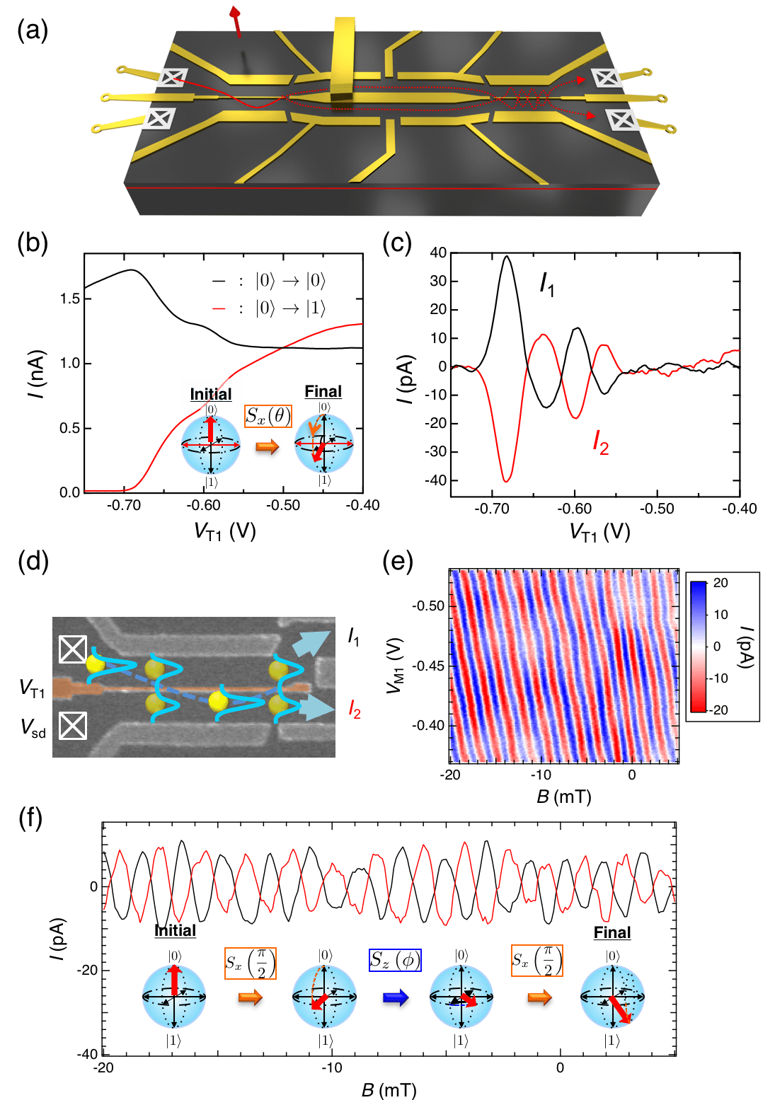
(ii)When and are set to large enough negative voltages to form a tunnel-coupled wire as schematised in Fig. 9(a), the behaviour drastically changes. The phase now smoothly evolves as a function of the the side gate voltage (Fig. 9(e)) while the output currents and show anti-phase oscillations (Fig. 9(f)). In this tunnel-coupled wire regime any superposition state of and in the AB ring can transmit into the tunnel-coupled wire by being transformed into the superposition of a symmetric hybridised state and an anti-symmetric hybridised state . This is in clear contrast with the above case of single wire leads, where only is transmitted into the leads. Scattering of electrons from one path to the other at the entrance and the exit of the AB ring are therefore highly suppressed and prevent electrons from encircling the AB ring several times and contributing to the interferenceBautze et al. (2014). These distinct behaviours depending on the tunnel-coupling energy have been also studied theoretically and nicely reproduced Bautze et al. (2014); Aharony et al. (2014). Consequently the device works as a true two-path interferometer as well as a flying qubit. Due to this peculiarity, this device has been exploited in recent studies to revisit a number of fundamental questions Schuster et al. (1997); Ji et al. (2000) about the phase modification of an electron when traversing a quantum dot Takada et al. (2014); Edlbauer et al. (2017).
In the tunnel-coupled wire regime a rotation about the x-axis can be performed as described in section I, where . This operation can be demonstrated by varying the voltage of gate which controls the tunnel-coupling between the upper and lower wire: A current is injected into the upper wire to prepare the initial state and the output currents and are measured as a function of the gate voltage (Fig. 9(b)). changes and hence the rotation angle . Clear anti-phase oscillations of currents and are observed at K, as shown in Fig. 9(c). These anti-phase oscillations are a direct signature of electron tunnelling between the two wires as schematised in Fig. 9(d). An electron injected into the upper wire oscillates between the upper and lower wire depending on the tunnel-coupling set by the gate voltage . For this device, the visibility of the oscillation, the ratio of the oscillation component to the total current, is limited to 1%. This is due to the existence of several transmitting channels and the high measurement temperature. Improvement of design and lowering the temperature allowed to reach visibilities above 10% Gregoire (2016).
A rotation about the z-axis can be achieved in the AB ring by varying the perpendicular magnetic field or the gate voltages as already outlined in section I. The relative phase difference between the upper path and the lower path is given by . The combination of and enables the generation of an arbitrary vector state on the Bloch sphere. This can be achieved by controlling simultaneously the tunnel-coupling and phase difference between the two paths.
is demonstrated in a Ramsey-type interference (Schematic in Fig. 9(f)). The two sets of tunnel-coupled wires were prepared to and the magnetic field is varied to perform in the AB ring. When the initial state is prepared to by injecting a current from the upper wire, the final state becomes
| (6) |
The two output currents are proportional to the square modulus of each coefficient and become
| (7) |
respectively. The measured and plotted in Fig. 9(f) indeed oscillate with exactly opposite phase for the modulation of by the magnetic field. The phase can also be modulated by the gate voltages , which changes the wave vector of the path. This is demonstrated in Fig. 9(e), where the phase smoothly evolves over a range of as a function of the side gate voltage along the vertical axis. This is in strong contrast to Fig. 8(d). This rotation about the z-axis by is important for qubit applications. Combined with the rotation about x-axis by , the qubit can be fully operated by the gate voltages at zero magnetic field. This allows for much faster operations than the ones controlled with a magnetic field.
The flying qubit presented here is attractive for quantum information technology. In addition to the ability to transfer the quantum information over a long distance, it has a much shorter operation time compared to other qubits in solid-state systems. The operation time (, gate length; , Fermi velocity) is of the order of ps. Analysing the temperature dependence of the oscillation amplitude shows that this qubit has a very long coherence length at mK Yamamoto et al. (2012). Using even higher quality heterostructures, the coherence length could be longer than . Since each quantum operation is performed within a scale, it would in principle be possible to perform more than 100 qubit operations.
On the other hand the visibility, defined as the AB oscillation amplitude divided by the total current, is limited to about %. Since the coherence length is found to be much longer than the interferometer length, decoherence is not the main origin of this limited visibility. The influence of thermal smearing due to the difference in Fermi velocity between the two paths is also small at the measurement temperature. The main limitation comes from the contribution of several transmitting channels in each part of the tunnel-coupled wires and in each arm of the AB ring while only one in each wire contributes to the main AB oscillation. Therefore the visibility could be improved by operating the interferometer with a highly coherent single transmitting channel (See Supplementary information in Ref. Yamamoto et al., 2012 for more details). One possible remedy towards this direction would be to adiabatically reduce the number of transmitting channels to one at a specific point of the interferometer while keeping the number of channels (or the electron density) constant over the other part of the interferometer. Higher electron density is preferable to screen the potential fluctuations induced by the gates, which is proposed to be the main source of decoherence in ballistic AB interferometers Seelig and Büttiker (2001), and hence to maintain the coherence.
In addition to quantum information transfer, it should also be possible to create a non-local entanglement state following the scheme proposed in refs. Yu and Voskoboynikov, 2008 and Ionicioiu et al., 2001b, combined with single electron sources Blumenthal et al. (2007); Fève et al. (2007); Hermelin et al. (2011); Dubois et al. (2013a) to synchronise qubits. This flying qubit can also be used in combination with a spacially localised qubit Schomerus and Robinson (2007).
In this section we introduced different device architectures which can be exploited to realise electronic flying qubits at the single-electron level. For the implementation of a flying qubit at the single-electron level, however, these architectures have to be combined with a single electron source as well as a single electron detector, which we will describe in the sections IV and V. In addition, synchronisation of different qubits is required to realise two qubit operations. For that purpose MZI in the quantum Hall regime is advantageous. Chirality suppresses backscattering and synchronising different single electron sources can be straightforwardly achieved Bocquillon et al. (2013a). Upscaling of this system, however, is not straightforward. On the contrary, the MZI interferometer for low magnetic fields is easier to scale-up by adding the basic qubit structure in parallel or in series. On the other hand, when the device gets longer, it will suffer from backscattering of the electrons, which prevents synchronisation between different qubits. One possible way to avoid backscattering is using electron transport by surface acoustic waves Barnes et al. (2000); Hermelin et al. (2011); McNeil et al. (2011); Hermelin et al. (2017); Ford (2017). The biggest challenge, however, is single shot detection of such single flying electrons. For low magnetic field there are potential approaches to achieve this in the near future (see section V) while single-shot detection under high magnetic field is a real challenge in this field of research.
When dealing with single-electron wave packets, it is also important that there is a substantial overlap between the interfering electrons at the output of a beam splitter Haack et al. (2011); Rosselló et al. (2015). It is hence important that the two inference arms are of similar length. For electron wave packets of a temporal width of about 100 ps, which can nowadays be routinely produced with state-of-the-art electronic equipment, the spatial extension is still large (10 m for a speed of 105 m/s). This is of the same order of magnitude as the size of the present interferometers. However, when going to smaller and smaller wave packets this issue has to be taken into account. The case where electron wave packets are much smaller than the size of the interferometer, new types of interference effects will appear Gaury and Waintal (2014). This novel physics will be described in section VII.
IV Single Electron Sources
In the preceding section we have presented proof-of-principle experiments for the realisation of a solid state flying qubit with two different types of MZIs. In these experiments, however, the electrons are injected as a continuous stream and the measurements are based on ensemble averages. The ultimate goal in this line of research is the ability to control the flying qubit at the single-electron level, which requires on-demand single electron sources (SES) as well as single electron detectors. In this section we will focus on the single electron sources which have been developed over the last 10 years with the goal to perform quantum interference experiments at the single-electron level.
At the origin of most single electron sources is the quest for a fundamental standard of electrical current linking the ampere to the elementary charge and frequency. Such single electron sources can be realised by high-speed, high-accuracy transport of single electrons in nanoscale devices Pekola et al. (2013); Kaestner and Kashcheyevs (2015); Kaneko et al. (2016). Development of an accurate single electron pump is of particular importance for metrology. It allows for the precise determination of the value of the elementary charge, which is one of the seven reference constants in the new SI units which will be redefined in 2018 des Poids et Mesures) (2010); Mills et al. (2011); Gibney (2017). In addition it contributes to the quantum metrology triangle (QMT) experiment Keller (2008); Feltin and Piquemal (2009) which is a consistency test of three quantum electrical standards: the single-electron current standard, the Josephson voltage standard and the quantum Hall resistance standard, which play a fundamental role in metrology. The future redefinition of the international system of units in terms of natural constants requires a robust, high-precision quantum standard for the electrical base unit ampere.
The best single electron pumps reach nowadays an error rate of better than 1 ppm at GHz Yamahata et al. (2016); Stein et al. (2017); Zhao et al. (2017). Besides this, integrated single-electron circuits have also a great potential in quantum information processing as already motivated in the introduction. Most implementations of today’s single electron sources are based on small isolated regions of charges connected to a reservoir via tunable barriers, a prime example is semiconductor quantum dots. In this case one exploits the fact that in a sufficiently small isolated region, the energy level is fully quantised by the charging energy originating from Coulomb interactions and the number of electrons inside the quantum dot can be controlled one by one Kastner (1992); Kouwenhoven et al. (1997); Reimann and Manninen (2002).
For completeness let us also mention that single electron transistors using superconductor or metallic islands have been developed to realise high accuracy current pumps Pekola et al. (2013). In this review, however, we will focus on single electron sources made from GaAs heterostructures.
IV.1 AC single electron source (Mesoscopic Capacitor)
A capacitor forms a simple and elegant possible realisation of a single electron source. The idea is to realise a RC circuit driven by an AC voltage such that the charge and discharge of the capacitor is limited to a single elementary charge . The capacitor has to be weakly connected to the lead in which the elementary charges are transferred such that charge quantisation occurs between two stationary capacitor states. A metallic island connected to leads by a single tunnel junction could realise this device when the Coulomb charging energy is larger than the thermal energy . However, the metallic island capacitor is reputed to have a quasi-continuous density of states and the energy at which, and the state from which electrons are emitted are not well defined, while controlling the initial state is of utmost importance for quantum information applications. A quantum coherent electron source requires in addition using a quantum dot viewed as a mesoscopic capacitor in which electrons keep quantum coherence and their state and energy levels are well defined. The spacing of the energy levels of the dots should be much larger than the thermal energy and the level used to emit and absorb single electrons, whose energy is closest to the Fermi energy of the leads, should be non degenerate. This coherent single electron source Fève et al. (2007) is based on a mesoscopic capacitor which was initially realised Gabelli et al. (2006) to check a prediction by M. Büttiker Büttiker (1993) of an universal quantisation of the charge relaxation resistance (called Büttiker’s resistance ). Here no DC current but only an AC current is produced. In the single electron source regime, a quantised AC current of amplitude is made of the periodic injection of single electrons above, followed by single holes below the Fermi energy . For ease of operation and further use in electron quantum optics, a strong perpendicular magnetic field brings the conductor in the integer Quantum Hall Effect (QHE) regime. In this regime, for a small dot (submicron diameter) the 1D QHE chiral edge states modes running along the dot boundary give rise to energy level quantisation with energy level spacing of typically 1 Kelvin in energy, where , a few cm/s is the drift electron velocity and is the quantum dot capacitor perimeter. The top gate, above the mesoscopic capacitor provides enough screening of the Coulomb interaction such that the charging energy is smaller than , see Fig. 10 for a schematic description. To ensure energy level and charge quantisation, the capacitor is weakly connected to the leads, the chiral edge channels, via a quantum point contact which controls the tunnel-coupling. The operating principle is as follows, see Fig. 10. Starting from a situation where the last occupied energy level is below the Fermi energy ①, a sudden rise of the voltage applied on the capacitor top gate rises the occupied energy level above the Fermi energy ②. After a time of the order of the energy-level life time , which is controlled by the barrier transmission , an electron is emitted at a tunable energy above the Fermi level ( is the energy level spacing). Then restoring the top gate voltage to its initial value ③ pulls down the energy level below the Fermi energy: an electron is captured or equivalently a hole is emitted at a definite energy below the lead Fermi energy. Fig. 10(b) shows time domain measurements of the measured current averaged over a large number of periodic emission cycles at a 30 MHz repetition frequency. The exponential decay of the current reflects the exponential decay rate (characteristic time ) of the emission probability of electrons and holes.
The mesoscopic capacitor electron source is an energy-resolved electron source. It provides a convenient single electron source where electrons can be emitted at a tunable energy () above the Fermi energy. The emission quantum energy uncertainty is also tunable, as reflected by the quantum emission time . Among major achievements obtained with the mesoscopic capacitor single source is the demonstration of single electron partitioning and the Hong–Ou–Mandel (HOM) correlations. Regarding limitations, for HOM experiments, it is technically difficult to realize identical capacitor dots due to nanolithography reliability. Another limitation is that a good energy resolution requires that the number of electrons (or holes) is limited to one per cycle because of the charging energy.
IV.2 Single electron pumps based on dynamic semiconductor quantum dots
As mentioned in the introduction of this section, the development of single electron sources have been triggered by the quest for a fundamental standard of electrical current. One of such sources realised in GaAs based nanostructures will be described in the following. The basic building block of this device is a dynamic quantum dot (QD), where the periodically varying confining potential is varied by energy barriers. Originally Blumenthal et al. (2007) such a source was implemented by using two barriers controlled by two independent voltage parameters. In a more optimised version Kaestner et al. (2008a); Fujiwara et al. (2008); Kaestner et al. (2008b); Fletcher et al. (2012) only one of the two gate voltages is used to eject a single electron from the dynamic QD as shown in Fig. 11.
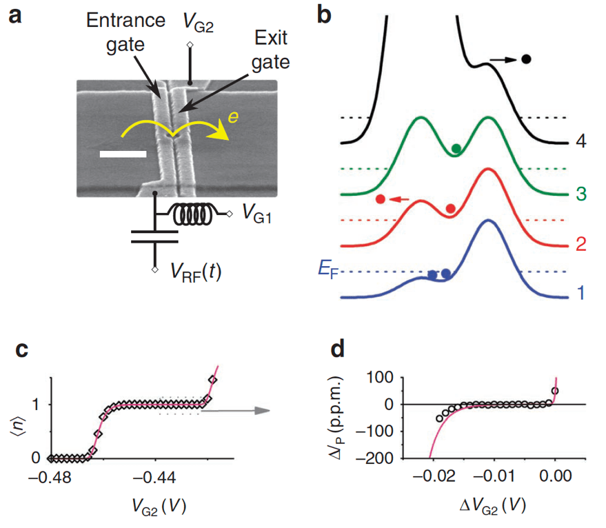
Two parallel electrostatic gates with a small opening allow to trap a small number of electrons inside the QD. A schematic of the one-dimensional electrostatic potential landscape is shown in the right panel. For the loading procedure the energy of the right barrier is set well above the Fermi energy to prevent the electrons from escaping the QD. The left barrier is then lowered to an energy close to the Fermi energy to load a small number of electrons (black curve). By increasing the gate voltage on the left barrier (more negative voltage) the QD is progressively isolated. During this process, some initially trapped electrons tunnel back to the reservoir before tunnelling is eventually suppressed. The electrons, which remain trapped, are ejected from the dot, once the left barrier exceeds the potential of the right one. By finely adjusting the voltages on the gate and it is then possible to eject a single electron. The single electron pumps are usually operated at a repetition frequency of 100 MHz-1GHz, limited by the tunnelling time into the QD. Presently, current accuracy of about 1ppm have been achieved Giblin et al. (2012). To obtain such a high accuracy, the experiments are usually done under a large magnetic field, which stabilises the quantised current plateaus as shown in 11(c) and (d) most likely due to the increased sensitivity of the tunneling rate to the electrostatic potential and the suppression of non-adiabatic excitations Leicht et al. (2011); Fletcher et al. (2013); Kaestner and Kashcheyevs (2015). Working at large magnetic fields is also convenient to guide the electrons along the edge states in the quantum Hall regime. A detailed review on the working principle and performance of these single electron sources can be found in ref. Kaestner and Kashcheyevs (2015). Let us emphasise that for this single electron source the electrons are ejected with an energy far above the Fermi sea, typically above 100 meV with an energy resolution of about 3 meV Fletcher et al. (2013). This is much larger than the Fermi Energy 10 meV as well as the charging energy of the gate defined QD 1meV. Naturally, this high energy will set limits to this single electron source to use it for electron optics experiments. We will come back to this issue at the end of this section.
It is also possible to measure the energy as well as the temporal distribution of the emitted high energy electrons. This can be done by adding an energy selective barrier at the arrival position Fletcher et al. (2013). By repeating the single electron emission at the pump clock rate and by inducing a time delay between the emission and the on-off switching of the arrival barrier, one can map out the shape of the emitted wave packet with ps resolution Waldie et al. (2015). Presently the smallest wave packet size so far detected is of the order of 5ps Johnson et al. (2017). Finally, it is also possible to load several electrons in the QD and eject them sequentially Fletcher et al. (2013). Using in a similar manner a barrier to detect the electrons it is possible to partition them individually Ubbelohde et al. (2015). We will come back to this issue in section VI.
Let us also mention that semiconductor devices made from silicon Takahashi et al. (2002) become again very popular Yamahata et al. (2016) for high precision electron pumps. This is also the case for single electron QDs which can be operated as charge Mi et al. (2017) or spin qubits M. et al. (2014); Maurand et al. (2016). Silicon has the advantage compared to GaAs that it can be relatively easily isotopically purified. Nuclear spin free 28Si is nowadays employed in the spin qubit field and extremely long coherence times have been obtained Muhonen et al. (2014).
IV.3 Single electron source based on voltage pulses (levitons)
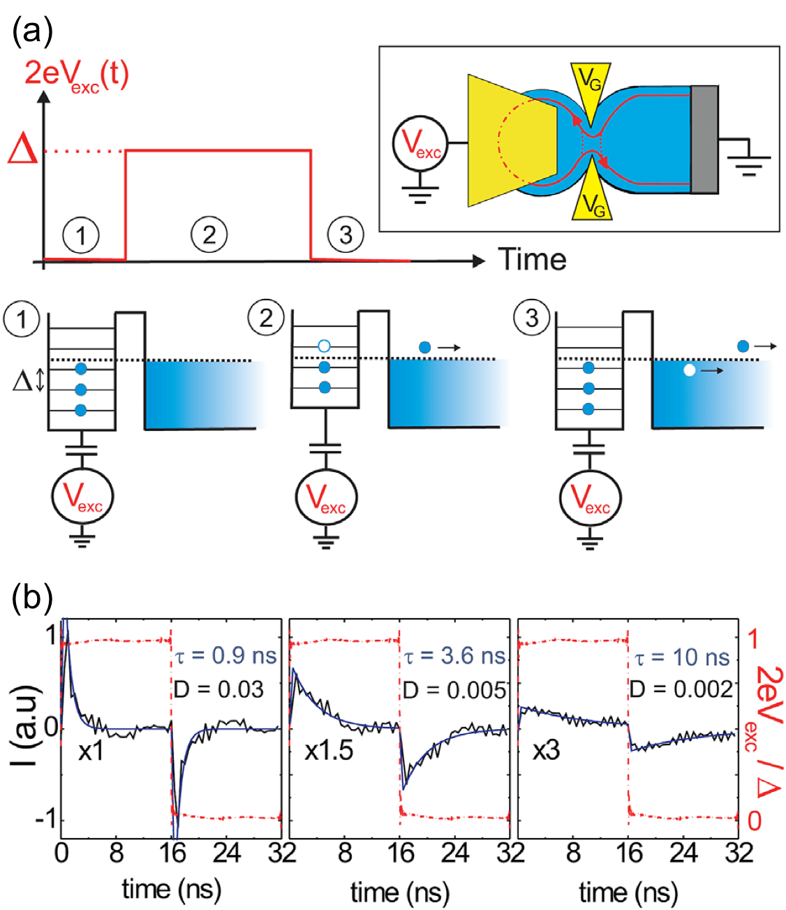
Here, we describe a very simple way of injecting single or multiple electrons in a quantum conductor. The idea is to reduce the charge emitted by the electronic reservoir to its ultimate value – an elementary charge – by applying an ultra-short voltage pulse.
The method presents the advantage that no lithography step is required for the electron source and the (moderate) difficulty is left to the control of a current pulse on a very short time scale. To describe the principle, let us first consider a perfect quantum conductor made of a single quantum channel, spin disregarded. According to finite frequency Büttiker’s quantum transport laws, a voltage pulse applied on a contact, while other contacts are grounded, injects a current pulse from the contact to the single channel conductor. To inject n electrons, one has to tune the amplitude and duration of the voltage pulse such that or equivalently . Thus realizing a single electron source () seems easy to perform. However, for quantum information application, it is important that the injected electron, the flying qubit, is the only excitation created in the quantum conductor. This is not the case in general, as noticed by Levitov and collaborators in a series of theoretical papersLevitov et al. (1996); Ivanov et al. (1997); Keeling et al. (2006). Indeed electrons are not injected in a vacuum of quantum states, like single photons, but on a ground state full of electrons, the Fermi sea. The voltage pulse in general perturbs all electrons and creates extra excitations Vanević et al. (2007, 2008, 2017). These excitations are neutral in order to conserve the injected charge. Levitov’s remarkable prediction was that only a special voltage pulse, a Lorentzian pulse, injecting an integer number of charge is able to provide a so-called minimal excitation state where only charge excitation is created with no extra neutral excitation Levitov et al. (1996). After its recent experimental realization Dubois et al. (2013a), this single charge minimal excitation state has been called a leviton. Other pulse shapesGabelli and Reulet (2013), or non-integer charge injection, create non-minimal states which are not suitable for flying qubits. To understand the underlying physics of the generation of levitons, one has to consider the effect of a voltage pulse on all electrons of the electrical contact subjected to the pulse. An electron emitted from the contact at some energy below the Fermi energy and experiencing the potential has its phase modulated as . As the time dependence is breaking energy conservation, the electron will end in a superposition of quantum states of different energies. The probability amplitude to have its energy displaced by is . For arbitrary phase modulation (or voltage pulse shape) takes finite values for both positive and negative . The electrons of the Fermi sea are displaced up and down in energy and this creates electron- and hole- like excitations. To create a leviton, a pure electron excitation with no hole, one needs for . To ensure this for a single pulse, must have no poles in the lower half complex plane and at least one pole in the upper half, i. e. . One immediately sees that the phase derivative (and so the voltage ) must be a Lorentzian, with :
| (8) |
the parameter is the width of the Lorentzian. Adding an extra pole in the upper complex plane is equivalent to adding an extra electron. For periodic leviton injection with period , the poles are regularly spaced at values , integer and and
| (9) |
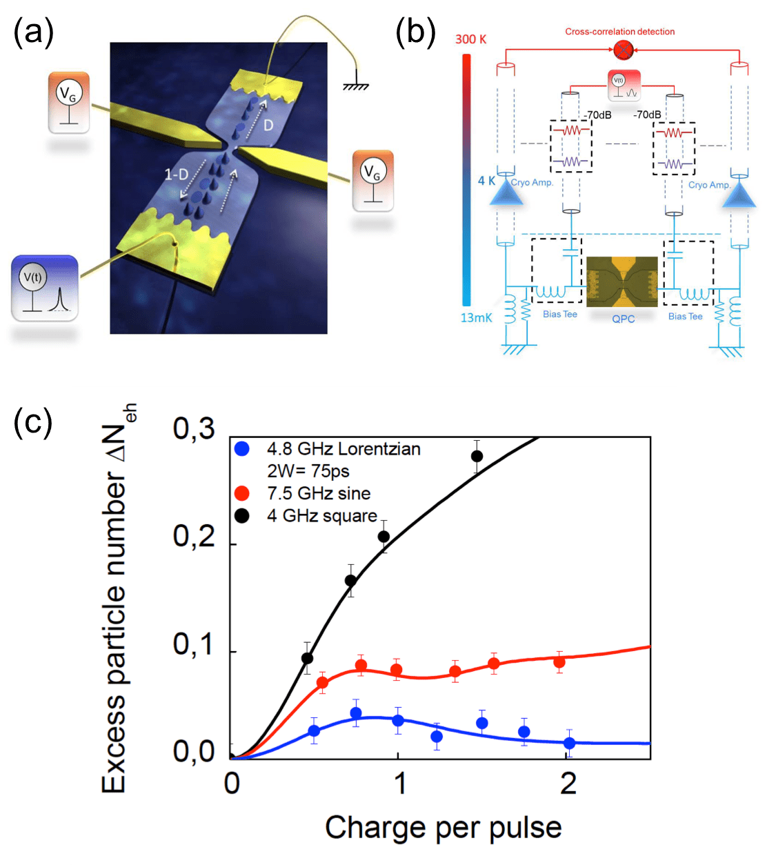
The first implementation of a single electron voltage pulse has been done recently, see ref. Dubois et al. (2013a). The periodic injection of a single electron, using square, sine and Lorentzian pulses have been compared to evidence Levitov’s prediction of minimal excitation states. To do this a measure of the total number of excitations created per pulses is needed. This is provided by sending the charge pulses towards a QPC with finite transmission . This artificial scatterer plays the role of a beam splitter which partitions the charge into transmitted and reflected states following a binomial law. Assuming we have created levitons, i.e. electrons not accompanied by electron-hole pairs, the partitioning statistics of electrons arriving at frequency gives a low frequency current noise spectral density (here ). If however both electron and hole excitations are incoming on the QPC, one can show that, at zero temperature, one has exactly, see ref.Dubois et al. (2013b) :
| (10) |
while the mean current is . Levitons with and give minimal noise. This was experimentally demonstrated in ref.Dubois et al. (2013a). Reduction of the shot noise has also been observed in experiments using tunnel junctions with a biharmonic drive Gabelli and Reulet (2013). In Fig. 12 (a) and (b), the experimental set-up is depicted: leviton pulses are sent on the ohmic contact of the quantum point contact, while partitioned quasiparticles are detected by cross-correlation measurement techniques. In Fig. 12 (c), excess particle number as a function of injected charge per pulse is shown: compared to the sine and square pulse, the Lorentzian pulse gives the smallest amount of electron-hole pairs. This approach ensures an excellent control of the electronic wave function that arrives at the QPC. For electron-quantum optics experiments, this source has the advantage to inject electrons at the Fermi energy and will less suffer from relaxation processes, as observed in the mesoscopic capacitor source. It is worth noticing that this experiment is an electron analog of a photonic Hanbury-Brown Twiss experiment Henny et al. (1999); Oliver et al. (1999) where single photons are sent to a beam splitter, but with electrons. We will see later that we can go further and perform Hong–Ou Mandel–interferometry by sending two periodic trains of levitons on each beam splitter input and measuring the noise correlation.
IV.4 SAW driven single electrons
Yet another highly efficient on-demand single electron source can be realised by transporting a single electron with a surface acoustic wave (SAW) Hermelin et al. (2011); McNeil et al. (2011).
One exploits again the fact that a single electron can be isolated in a semiconductor quantum dot (QD) and single electron transfer can be realised by transferring the single electron into a moving SAW QD.
When connecting two QDs with a quantum channel (see figure 13(a)), it is then possible to transfer a single electron from one QD to the other with detection efficiencies much higher than 90 % Hermelin et al. (2011); McNeil et al. (2011).
GaAs is a piezo-electric substrate and therefore allows to generate SAWs which carry a moving electric field for certain crystal directions.
The SAW can be generated by an interdigitated transducer (IDT) which is deposited on the surface of the GaAs substrate (see figure 13(b)).
The IDT is usually composed of several tens of interdigitated metallic fingers with a length of about 100 m in order to create an oscillating electric field at the surface of the GaAs crystal when applying a radio frequency signal to the two electrodes.
Due to the piezo-electric effect, the crystal contracts periodically and generates a Rayleigh wave for specific crystal directions which travels at the surface of the GaAs crystal with a sound velocity of the order of 3000 m/s De Lima et al. (2003).
This slow speed, which is about 2 orders of magnitude slower than the Fermi velocity, is advantageous as it allows to induce gate operations of the propagating electrons on shorter length scales compared to ballistic electrons.
The wavelength of the SAW can be simply engineered with the distance between the fingers of the IDT.
For such single electron transfer experiments, the IDT is operated at a frequency close to 3 GHz which translates into a wavelength of the order of 1 m Shilton et al. (1996); Talyanskii et al. (1997); Naber et al. (2006); Bertrand et al. (2016b).
This ensures a moving QD of a size of several hundred nanometers when propagating through an electrostatically defined one-dimensional channel of similar dimensions.
Going to higher frequency is desirable as it increases the confinement potential and hence the level spacing of the QD.
This however comes with technical difficulties.
Beyond a frequency of 5-6 GHz the efficiency of the IDTs decreases drastically due to ohmic losses in the metal strips (usually made from gold) but also due to losses into the bulk of GaAs.
The wavelength gets so small that surface roughness can excite bulk waves.
Going to smaller wavelength puts also much higher constraints on the spatial resolution of nanofabrication.
The highest frequencies which have been achieved (f 20 GHz) so far have been realised with nano-imprint techniques Büyükköse et al. (2012).
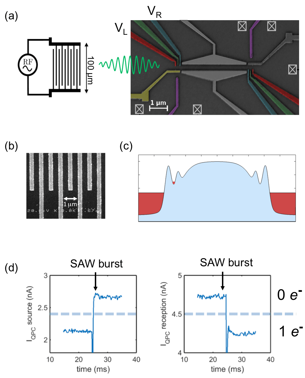
The SAW driven single electron source is operated in the following way: At first, a single electron is loaded into the QD at the loading position LP of the charge stability diagram shown in figure 14 (c). The quantum point contact (yellow and purple gates in figure 13(a)) allows to detect whether an electron is present inside the QD (see section V for details). Varying gate voltages and the electron is then moved to its isolated position IP by increasing the barriers formed by the electrostatic gates which separate the QD from the reservoir () and the channel (). At this position the electron can be trapped for a very long time Bertrand et al. (2015). The dwell time of an electron in this isolated position can be measured by statistical average of the time when the electron stays in the QD before it tunnels into the nearby reservoir. This is shown in figure 14(d) where several individual escape events are measured. Averaging 10000 of such events results in an exponential decay from which one can deduce the dwell time of the electron in the isolated position, here 700 ms.
If one now keeps an electron in the isolated position and launches a SAW train, one can expel the single electron from the QD with very high efficiency. To demonstrate this, a 60 ns long SAW train is launched from the IDT 50 ms after the single electron is brought to the isolated position. If the amplitude of the SAW is sufficiently strong, the moving electric field can pick-up the electron from the QD and carry it along. This is shown by the red curve in figure 14(e). Whenever the SAW arrives at the QD, the electron is ejected and the QD is depopulated. Adjusting the SAW amplitude and the QD potential, ejection efficiencies higher than 96 % have been achieved Hermelin et al. (2011); McNeil et al. (2011). By engineering one-dimensional channels with electrostatic gates, the ejected electron can be transported and guided at will to any desired position on the electronic circuit. The single electron is then literally surfing on the SAW within the electrostatic confinement potential landscape created by the one-dimensional channel as shown in figure 13(c). In order to show that the electron is indeed transferred to the detector QD through the one-dimensional channel it is necessary to perform coincidence measurements on both QDs at the same time Hermelin et al. (2017). Such coincidence measurements are shown by the QPC traces in figure 13(d) .
Now that we have presented the different single electron sources let us discuss their advantages and disadvantages. All four SES can easily be integrated into electronic quantum circuits engineered from GaAs heterostructures. The leviton source has the least constraints on nano fabrication as it simply requires an ohmic contact to which a short voltage pulse is applied. Care has to be taken for the design of the waveguide which guides the radio-frequency (RF) signal to the contact, but this is true for any electrical connection on-chip which is operated at RF frequencies. The ohmic contact should be reduced to a small size, typically mm, to be able to easily guide the single-electron wave packet into a gate defined quantum rail and the contact resistance should be as small as possible, typical values are of the order of 100 . For all other sources, several additional electrostatic gates have to be implemented. The most demanding from this point of view is certainly the SAW based single electron source as it requires a detector (QPC) as well as a QD to make it operational. On the other hand an important advantage of this SES is that it also allows for single-shot detection, a requirement absolutely necessary for quantum information purposes. For this single electron transport technique it is possible to capture the propagating single electron in another QD and measure its presence with a single-shot measurement Hermelin et al. (2011); McNeil et al. (2011) with a precision higher than 99 % Takada et al. (2016). This is presently not the case for the other three electron sources. All electron counting experiments performed to date with these SES are based on a measurement of the average DC current or the low frequency current noise while repeating the experiment billions of times. To reach the single-shot limit is very challenging since the propagation speed of the generated electron is very fast and the interaction time with any detector will be very short (see next section for details).
To realise a current standard the non-adiabatic charge pump is obviously the best choice as it allows quantisation of the electron charge as well as very high clock frequencies. SAW based single electron sources as the one presented here cannot be operated at very high repetition frequencies. Presently they are limited to below Hz due to technical issues of the experimental setup Hermelin et al. (2017). It is also possible to apply the SAW in a continuous manner by driving the SAW across a constriction Wixforth et al. (1986); Shilton et al. (1996); Ford (2017) rather than by single electron transport between QDs with very short SAW bursts. In this case one can confine a single electron within each minimum of the SAW. and allows to obtain a very high repetition frequency (several GHz). This technique was initially developed with the motivation to realise a very precise electron pump with a current of several hundred pA (1GHz 160 pA). The best precision which could be achieved with this source was, however, only of the order of 100 ppm Ford (2017). For quantum interference experiments single electron transport using a SAW wave in a continuous fashion presents also some limitations. The power dissipation due to the SAW itself is high, not favourable for quantum interference experiments. Neither the leviton source nor the Mesoscopic Capacitor source can be used as a current standard. The leviton source does not deliver any quantised current, that is no quantisation plateau will appear when changing for instance the amplitude of the voltage pulse, while the Mesoscopic Capacitor source delivers a zero net DC current as it periodically generates an electron followed by a hole.
In this review, however, we are mainly interested in discussing quantum coherent nanocircuits suitable for implementation of electron quantum optics and flying qubits with electrons. This requires an electron wave packet that preserves its phase while propagating throughout the entire quantum circuit. In addition, two electrons sent from two different sources should be well synchronised in time and should be indistinguishable. In this respect the four SES have quite different properties. Synchronization on the ps level can be achieved with all four single electron sources. State-of-the-art arbitrary wave generators allow to induce a time difference of presently of about 1 ps between two output signalsJohnson et al. (2017) which is well below the actual time-spreading of the generated single-electron wave packets. In this respect only the synchronisation of the SAW wave source seems problematic as a single electron has to be loaded into exactly the same SAW minimum for each SES. Recent experiments have shown that this can be achieved with very high efficiency when using ps pulse triggering of the loading barrier gate to inject an electron into a specific minimum of the SAW train Takada et al. (2016). With this technique it is then possible to map out in a time-resolved manner the entire SAW train.
An important issue for realising quantum interference experiments at the single-electron level is phase preservation. For the non-adiabatic SES, the ejection energy of the electron is very high. While propagating, the electron will relax and loose energy which results in visibility loss when performing interference experiments. It has been shown that electrons can be transported over several microns with small inelastic electron-electron or electron-phonon scattering Fletcher et al. (2013). For a 170 meV emission energy the contribution due to inelastic scattering is less than 1 meV. In order to reduce energy relaxation over longer propagation length, it is possible to completely deplete the electron gas which minimizes electron-electron interactions Kataoka et al. (2016). Interference experiments with such a SES, however, have not yet been reported. Energy relaxation is also an issue for the Mesoscopic Capacitor electron source. Similar to the non-adiabatic single electron source, the generated electron have a well defined energy, however with a 100 times smaller energy. Still, when launching the electron wave packet, it will relax in energy during propagation which will lead to decoherence Roussel et al. (2017); Ferraro et al. (2013). In addition electron-electron interaction between the edge channel have to be taken into account. Even though additional edge channels help to reduce the Coulomb interaction due to mutual screening Gurman et al. (2016), Hong–Ou–Mandel interference measurements show that the Pauli dip does not go to zero Bocquillon et al. (2013a). We will come back to this issue in more detail in section VI.
This issue is conceptually different for the other two sources. As mentioned above, the leviton source generates a very peculiar type of single electron excitation. Due to its exponential energy distribution, the leviton lives very close to the Fermi sea and since all electronic states below the Fermi sea are occupied, it is well protected against energy relaxation. Two particle Hong–Ou–Mandel interference have shown a reduction of the Pauli dip which is in good agreement with theoretical expectations Dubois et al. (2013a) and nicely demonstrates that the two emitted electron wave packets are indistinguishable. From these experiments it is however difficult to estimate a value of the phase coherence length. Preliminary experiments on a 40 m long tunnel-coupled wire with electron wave packets of a temporal width shorter than 100 ps have shown that phase coherence is preserved throughout the wireGregoire (2016). This is very promising and suggests that the leviton source is very suitable for integration into a flying qubit architecture. Apart from being very suitable for quantum optics like experiments, the leviton source will also allow to explore novel quantum effects. As the wave packet is propagating at the surface of the Fermi sea, novel quantum interference phenomena have been predicted when a very short charge pulse is interfering with the Fermi sea Gaury and Waintal (2014). This novel physics will be discussed in section VII
The SAW electron source on the contrary eliminates completely the effect of the Fermi sea. The electron is confined in a moving QD well above the Fermi energy. In this sense this technique is the closest to photon experiments. However, the fact that the electrons are completely isolated form the Fermi see makes them also more vulnerable to external perturbations since electron screening is strongly reduced. As mentioned above, this technique allows to transport single electrons with a very high fidelity Hermelin et al. (2011); McNeil et al. (2011). Recent experiments have been able to push the transfer efficiency beyond 99 % for a transfer distance of more than 20 microns Takada et al. (2016). Employing a structure similar to the one schematised in figure 1(a), it has been possible to partition on-demand electrons coming from input port 1 into the two output ports, hence realising a directional coupler at the single-electron level Takada et al. (2016). Present research is devoted to the realisation of phase coherent transport of SAW driven electrons. First attempts for the observation of coherent tunnelling between two tunnel-coupled wires have been done with a continuous wave approach. In these experiments tunnelling from one quantum wire into a two-dimensional reservoir have been observed Kataoka et al. (2009); Ford (2017). Coherent tunnelling between two tunnel-coupled wires with SAWs have so far not been realised. This is subject to ongoing experimental research. Finally, let us also mention that single electron transport assisted with SAW also allows to exploit the spin properties of the electron which is quite appealing for quantum information processing. The spin degrees of freedom couple much less to the electromagnetic environment compared to the charge degree of freedom. Recent measurements have shown Bertrand et al. (2016a) that the spin polarisation is preserved during the transport with a fidelity of 70 %.
V Single Electron Detectors
The detection of a single electron can be achieved when the electron is captured inside a static quantum dot. As the electron can be trapped for a sufficiently long time, it can be detected with conventional on-chip detectors Field et al. (1993) and which we will detail below. In quantum experiments Ji et al. (2003); Roulleau et al. (2008a); Yamamoto et al. (2012); Bocquillon et al. (2013a); Dubois et al. (2013a), where one would like to detect the electrons on the fly, this task is much more difficult: indeed the interaction time with any detector usually does not exceed 1 ns and is fixed by the speed of the flying electrons, the size of the on-chip detector and the spatial extension of the electronic wave packet. This issue will be addressed in more detail in section V.2.
V.1 Single electron detection in static quantum dots
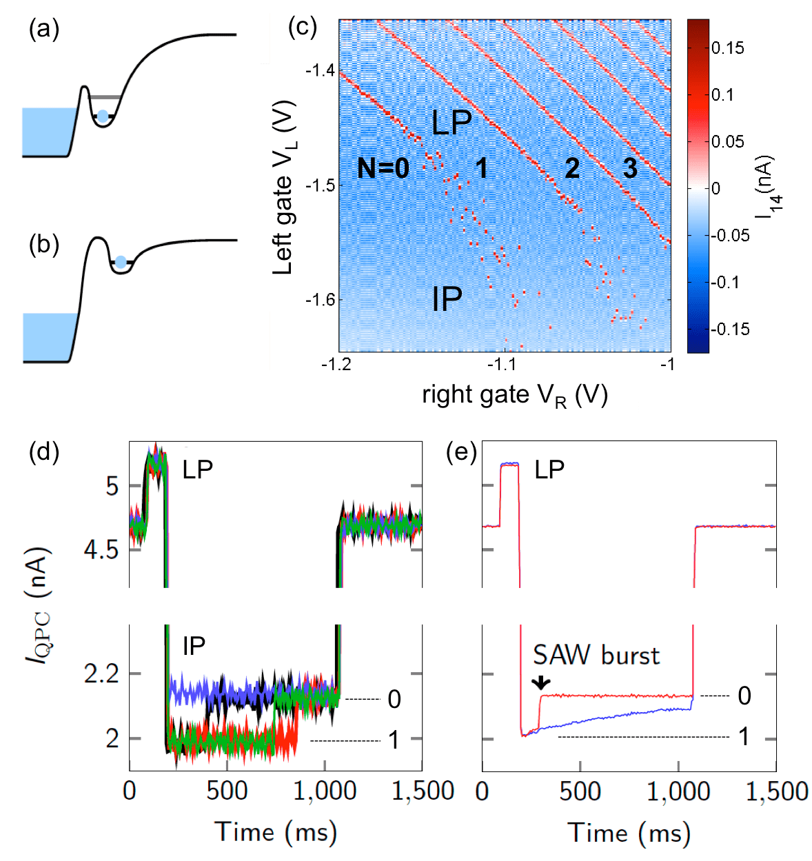
A very convenient way to read out the electronic charge state of a static quantum dot can be realised by a quantum point contact Field et al. (1993) when placed in close vicinity to the quantum dot (QD) (see figures 13 and 15). The quantum point contact (QPC) is brought to a gate voltage condition where the sensitivity G/ is the highest, usually in between the first quantised plateau and the pinch-off as shown in figure 15(b). The QPC is biased typically at a few hundred microvolts to avoid back action Leturcq et al. (2009); Granger et al. (2012) and the current through the QPC is continuously monitored. At this working point the current is very sensitive to the nearby electrostatic environment. If the electron number of the quantum dot is changed, the nearby electrostatic environment will be modified and results in an abrupt variation of the QPC current as shown in figures 15 (c). When sweeping the two side gates ( and ) of the QD shown in figure 13(a) and 15(a), one can map out the so-called charge stability diagram Kouwenhoven et al. (1997) of the QD. Plotting the derivative of the conductance with respect to the gate voltage to suppress the smooth background and to enhance the conductance steps, one observes parallel lines which delimit regions where the electron number is constant. Whenever a diagonal line is crossed, the number of electrons changes exactly by one. Decreasing the voltage to more negative values ejects the electrons one by one until one ends up with a QD containing no electron at all (large region on the left in figure 15 (d) where the diagonal lines are absent).
Nowadays the QPC is often replaced by a sensing QD where one takes advantage of a very sharp Coulomb blockade peak, which can have a higher sensitivity G/. In this case the sensing QD is operated at a very steep flank of a Coulomb peak. This requires, however, an additional gate to be added to the sample design. In addition to these improvements, fast read-out schemes have been implemented by reflectometry in order to increase the measurement bandwidth. To do so, the QPC or QD is integrated into a LRC tank circuit which operates at a few hundred MHz. This is the so-called RF-QPC which allows for single-shot detection at timescales below 1 s. Müller et al. (2007); Reilly et al. (2007); Cassidy et al. (2007).
V.2 Towards single electron detection on the fly
To detect an electron on the fly is presently the most challenging task in the field of electron quantum optics. First, the interaction time between a submicron-size electrometer and the flying electron does not exceed 1 ns and is fixed by the speed of the flying electrons, the size of the on-chip electrometer and the width of the electronic wave packet. This interaction time is 2 orders of magnitude faster than the typical timescale needed to detect a single electron for the best on-chip charge detector demonstrated so far in a 2DEG Barthel et al. (2009); Dial et al. (2013). Second, the experiment has to be performed at temperatures below 50 mK to avoid fluctuations of the local chemical potential of the Fermi sea larger than the influence of a single electron on the detector Levitov et al. (1996).
Combining single electron injection and readout would open the avenue for the realisation of full quantum experiments and will bring the field of electron quantum optics to a status similar to that of quantum optics. In particular, single-shot detection of flying electrons would enable to perform electron flying qubit operations.
Up to now most measurements are statistical: electron injection is periodically repeated and DC current or low frequency current noise measurements provide information on the average value and the fluctuations of the charge that arrives in each contact. Recording the detected single charge each time, when a single charge is injected, will also give unprecedented access to the Full Counting Statistics of the electron partitioned between the different output arms of an interferometer. In addition, due to the existence of Coulomb interaction electrons provide new possibilities for linear quantum optics Knill et al. (2001); Beenakker et al. (2004) especially to generate entanglement Ionicioiu et al. (2001a).
Towards this goal several quantum systems have been identified as extremely sensitive systems to external perturbations and potentially good detectors Gleyzes et al. (2007). They have been used for example to detect a single phonon excitation of a nanomechanical system O’Connell et al. (2010). In a 2DEG, two quantum systems have been recently proposed to detect propagating electrons: a double quantum dot charge qubit and a Mach-Zehnder interferometer Neder and Marquardt (2007).
Another option is to exploit the extreme sensitivity of spin qubits when operated in the charge regime. The idea is to couple capacitively the single flying electron to a so-called Singlet-Triplet (S-T0) qubit Thalineau et al. (2014). The two levels of the qubit are the two anti-parallel spin states of a double quantum dot with one electron in each dot Petta et al. (2005). For such a spin qubit, the energy separation J is directly related to the exchange interaction. J is highly dependent on both, the energy detuning between the two dots and the tunnel-coupling and can be widely tuned on fast timescale in lateral double quantum dots in GaAs heterostructures Hanson et al. (2007). In more recent experiments it has been shown that the the tunnel-coupling can be tuned over an extremely large range, from basically zero to several GHz Bertrand et al. (2015); Martins et al. (2016); Reed et al. (2016). The S-T0 qubit can hence be used as an ultra-sensitive detector to probe the local electrostatic environment Dial et al. (2013). These properties can be exploited to imprint the passage of the flying electron on the qubit population where it can be stored for several microseconds.
The principle of this flying electron detector is depicted in figure 16. An electron, which is guided via electrostatic gates or the edge channels in the QH regime is passing by the S-T0 charge detector schematically shown as a double dot. Due to the capacitive coupling between the electron-wave packet and the detector, the electrostatic environment of the quantum dot will be slightly modified. This leads to a change of the qubit energy splitting during the interaction time. As the Rabi oscillations (see figure 16(b)) accelerates for more positive energy detuning, the passage of an electron close by to the detector will induce a phase shift in the rotating frame of the S-T0. The accumulated phase shift corresponds to a population change of the S-T0 qubit. If the accumulated phase is this would correspond to a complete flip of the S-T0 population. Such a change in population can be stored for several tens of microseconds in the spin degrees of freedom of the qubit and then be measured single-shot by spin-to-charge conversion. Ideally, if the coupling is large enough to ensure a phase shift, a one-to-one correspondence between the qubit state and the presence of the flying electron is expected and therefore a single-shot detection of the flying electron can be performed. The challenge here is to reach a large enough phase shift to have the sensitivity to detect a single flying electron in a sub-nanosecond timescale. First attempts have been done in this direction Thalineau et al. (2014) and report a phase shift when a packet of 80 flying electrons is passing by the detector. Improved sample design should allow to reach in the near future the detection of a single electron on the fly.
VI Quantum optics like experiments with single electrons
Photons are very interesting flying particles to study quantum effects such as entanglement, non locality or quantum teleportation Bouwmeester et al. (1997); Pan et al. (1998, 2000). One can produce single photons on-demand, single-photon detection can be realised after propagation and most importantly its coherence can be preserved over hundred kilometres Ma et al. (2012); Korzh et al. (2015). Important tools with which to infer complex photon correlations inaccessible from ensemble measurements are single photon sources and single photon detectors. They are also the elementary building blocks for the manipulation of information coded into a quantum state, a qubit. When combined with beam splitters, polarisers etc., photonic qubits can be manipulated to process quantum information. A well-known example is quantum cryptography Bennett et al. (1992); Gisin et al. (2002), a secure way to transmit information. On the other hand, it is very difficult to make two photons interact and this represents a crucial technological hurdle for producing more complex quantum operations with photons. Several strategies towards this goal have been proposed based on optical cavity QED concepts, however it turned out to be very challenging experimentally Reithmaier et al. (2004); Yoshie et al. (2004). An interesting concept has been brought forward to realise efficient quantum computing with linear optics. In this case the combination of beam splitters, phase shifters, single photon sources and photo-detectors with feed forward control allows to implement efficient quantum computation Knill et al. (2001), where two qubit operations can be performed probabilistically by measurement of photons O’Brien et al. (2003); Politi et al. (2008); Carolan et al. (2015). In analogy with photons, similar experiments should be possible with single flying electrons in a solid-state device. The advantage of performing quantum optics experiments with flying electrons is the existing Coulomb coupling between the electrons. Photons are basically non-interacting quantum particles and they therefore have a longer coherence time than electrons. However, due to the absence of interactions it is more difficult to construct a two-qubit gate, which operates at the single photon level. This represents some fundamental limitation to the development of quantum computation with photons. In contrast Coulomb interaction allows to envision deterministic two qubit operations for electrons at the single-electron level Ionicioiu et al. (2001a); Beenakker et al. (2004). Naturally, strong interactions come with a short coherence time and may set limitations to this system for quantum information processing. We have seen in section III that quantum operations can be done on a very fast time scale for ballistic electrons, allowing in principle to perform about one hundred quantum operations on the fly. Yet, this research field is only at its beginning and much technological development is still needed in order to bring it to the level of its photonic counter part. We have seen, however, that single electron sources have an extremely high efficiency, well above what it is possible at present with single photon sources. The best on-demand single photon sources are based on quantum dots integrated into optically resonant micro-cavities Claudon et al. (2010); Somaschi et al. (2016); Ding et al. (2016). They offer a high degree of indistinguishability and a collector efficiency of approximately 65 . Integration and synchronization of multiple single photon sources into multiple photonic waveguidesArcari et al. (2014) by keeping at the same time a high emission efficiency, a high degree of indistinguishability as well as a high brightness is a real challenge. The same is true for the integration of single photon detectors into photonic wave guide structuresAkhlaghi et al. (2015). On the other hand, single electron detection is much more challenging compared to photons when dealing with single electrons propagating at the Fermi sea. In addition, an important question is how good a quantum state one can prepare and how well it can be preserved upon propagation. This is subject to ongoing experimental as well as theoretical research. Nevertheless the possibility to exploit single electron circuitry for quantum information processing merits to be explored to see how far this technology can be pushed. Besides that, we will also see that a lot of other interesting physics arises due to the interaction of the single electrons and the Fermi sea Blanter and Büttiker (2000). In the following we will present the present state of the art concerning such electron quantum optics experiments.
VI.1 HOM interference in quantum Hall edge channels
Since the seminal work of Hong, Ou and Mandel (HOM) Hong et al. (1987), HOM interferometry is commonly used in photonic quantum optics. HOM interferometry is a two-particle interference (or second-order coherence) which tests the indistinguishably and the quantum statistics of single particles. It consists in sending repeatedly two particles at the two separate inputs of a beam splitter and looking at the arrival coincidence in the two separate outputs. A time delay is introduced between the incoming particles. For , the particles are fully indistinguishable and fully mix in the beam splitter.
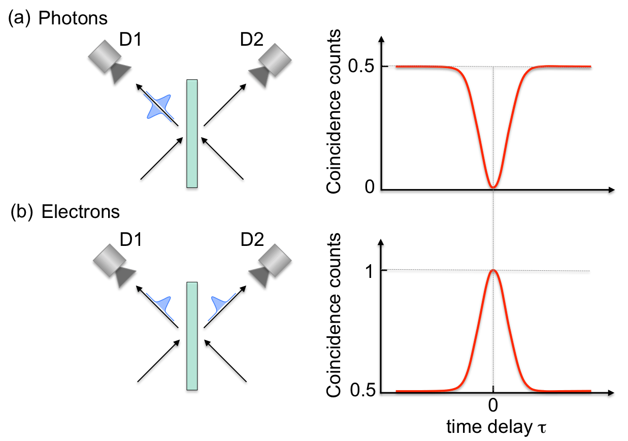
According to the fact that photons are bosons, the positive quantum statistical interference makes them to appear simultaneously in one of the two detectors. This is the so-called photon bunching. As a consequence the coincidence counts between the two output ports are fully suppressed. By varying the time delay between the emitted photons as shown in figure 17, the overlap of the wave function between the two arriving single particle states can be measured. The overlap is maximal when the particles arrive simultaneously at the beam splitter while it tends to zero when the time delay becomes larger than the wave packet. Looking at the particle number fluctuations, the noise in each output corresponds to binomial partitioning of two particles and is doubled with respect to the case where only a single particle were sent to the beam splitter. This is the limit which is recovered if the time delay is much longer than the extension of the photon wave packet . In the intermediate range of the noise is . For particles obeying fermionic statistics, a similar effect occurs, which however leads to the opposite behaviour Blanter and Büttiker (2000). Destructive quantum statistical interference makes them never appearing in the same output for . This is the Pauli exclusion as opposed to photon bunching. Thus, if we send periodically single electrons in an electron beam splitter one expects a low frequency current noise .
Electronic HOM like experiments have been done using DC voltage sourcesHenny et al. (1999); Oliver et al. (1999); C. Liu et al. (1998) but they were incomplete as there was no way to provide time control. In contrast, the advent of on-demand single electron sources allow performing full HOM interferences. The first HOM experiment at the single-electron level has been done using the mesoscopic capacitor single electron source Bocquillon et al. (2013a) operated in the quantum Hall regime. Two electrons are injected into the quantum Hall edge channel from each single electron source as shown in figure 18. It is possible to guide the electrons along the edges towards a beam splitter where they interact and then detect them at the two output ports. This set-up is the electronic equivalent of the photonic Hong–Ou–Mandel (HOM) Hong et al. (1987) experiment, where two photons are colliding on a beam splitter.
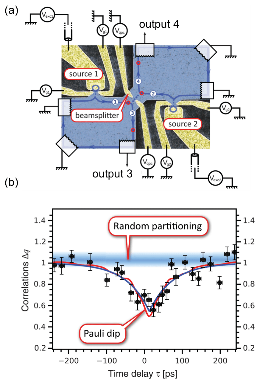
Electrons arriving at the same time at the beam splitter will exit in different output ports (anti-bunching). However, single-shot measurements of the arriving electrons, as for the case of photons, is at present not achievable. For this reason, the anti-bunching is probed by the measurement of low-frequency fluctuations of the electrical current in the two output leads rather than by coincidence counts. Two identical quantum dots are placed at a distance of approximately 3 m away from a quantum point contact tuned to a transmission and which acts as a beam splitter. For the present experiment, the average emission time for both single electron sources were fixed to 58 7 ps and the low frequency partition noise is measured by repeating the measurement at a frequency f 2 GHz. As mentioned in section IV, for this single electron source, at each cycle one electron is emitted followed by a hole. The low frequency current noise Blanter and Büttiker (2000) at one of the outputs is then given by Jonckheere et al. (2012) . By changing the time delay of the electron emission of the two sources, one can then probe the indistinguishability of the electrons coming from the two single electron sources. This is shown in figure 18b, where the excess partition noise is plotted as a function of the time delay . At large delays, one essentially measures the random classical partition noise as indicated by the blue shaded line. For short time delay one observes a dip in , which corresponds to the fermionic equivalent of the HOM dip, and, which clearly demonstrates two-particle interference effects. The dip, however, does not go to zero for zero delay as for the case of indistinguishable photons but stays at a finite value. The particles arriving at zero time delay at the beam splitter have hence lost a certain degree of indistinguishability. While the two-particle interference effect was clearly observed, the HOM dip at was not fully developed as decoherence occurred and prevented full indistinguishably. The origin of the finite excess noise at zero delay originates from Coulomb interaction effectsWahl et al. (2014); Rech et al. (2016) between the different edge channels as the experiment has been realised in the quantum Hall regime at filling factor . Even though a single electron is injected into the edge channel closest to the edge of the sample, during propagation inter-channel coupling leads to a loss of coherence towards the other channels and results in a reduction of the HOM dip Wahl et al. (2014); Rech et al. (2016). This has been investigated in more detail recently Freulon et al. (2015) for the case of filling factor . When injecting an electron into the outer edge channel, due to Coulomb interaction the electron wave packet decomposes into new propagation modes that couple both channels: a slow neutral mode where the charge is anti-symmetrically distributed over the two channels and a fast charge mode which has a symmetric charge distribution Levkivskyi and Sukhorukov (2008). This leads to additional dips in the HOM curve at time delays which correspond to the difference of the propagation velocities of the two different modes Bocquillon et al. (2014). This has also been addressed recently by time resolved measurements Kamata et al. (2014). We will come back to this point in the outlook section.
VI.2 HOM interferometry with levitons
Another HOM experiment, which we describe in this section has been performed with levitons Dubois et al. (2013a) propagating in the single channel of a QPC at zero magnetic field, a situation less sensitive to interaction induced decoherence. In addition, levitons live close to the Fermi energy, which increases their coherence time.
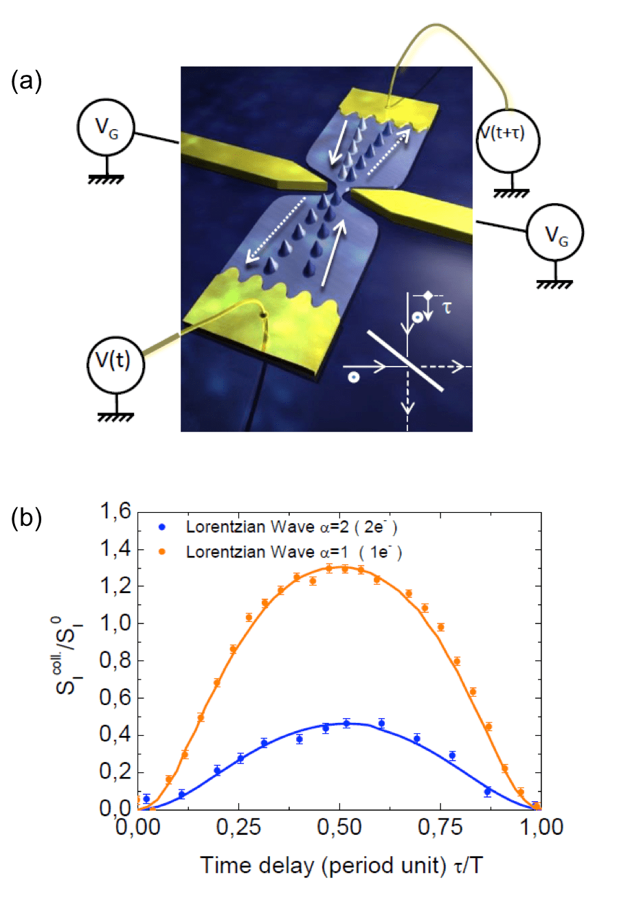
Figure 19 shows the schematic principle where two periodic Lorentzian pulses are injected with a controlled time-delay on opposite contacts of a QPC beam splitter. The two trains of levitons interfere and mix in the electron beam splitter and the cross-correlated noise is measured. Here single and doubly charged levitons are considered. At zero temperature one expects that the noise gives direct information on the overlap of the leviton wave functions. It is given by:
| (11) |
where is the leviton wave function. If doubly charged levitons are sent, one expects:
| (12) |
where are the first two orthogonal levitonic wave functions Glattli and Roulleau (2016) of a Slater determinant describing the two incoming electrons. Finite temperature only slightly reduces the amplitude of noise variations with , not the shape. Remarkably, the voltage pulse electron injection technique allows the generation of an arbitrary number of electrons and to perform a N-electron HOM correlation. In figure 19 experimental HOM measurements are shown (points) and compared with theory (solid curves) with no adjustable parameters for single and doubly charged interfering levitons.
HOM experiments have also been performed with a tunnel junction driven by a harmonic time-dependent voltageVanević et al. (2016). Beyond HOM experiments, electron quantum optics with single electron sources allows to perform all quantum experimental standards of quantum optics. Closely related to HOM interference, is the Quantum State Tomography (QST). The goal of QST is to give a complete view of the electron wave function. It consists in measuring the energy density matrix from which the Fermi sea contribution has been subtracted. From this, one reconstructs the Wigner function which, in the representation of the conjugate energy-time variables , is given by
| (13) |
For periodic injection, only the non-diagonal elements of differing by a multiple of the fundamental frequency are non zero. This implies that the Wigner function is a periodic function of time and this conveniently restricts the number of measurements to be done. A quantum state tomography procedure to measure has been theoretically proposed by Grenier and collaborators Grenier et al. (2011); Ferraro et al. (2013). This has been experimentally realised in Ref. Jullien et al. (2014). The measurements were only able to sample the first two harmonics of the Wigner function, although the third might have been accessible as well. The theoretical Wigner function restricted to two harmonics is compared with the experimental one in figure 20. This example shows the degree of maturity that has reached electron quantum optics today.
VI.3 Electron partitioning experiments (non-adiabatic quantised charge pump)
Finally, let us also mention another way of partitioning electrons that can be realised by using an energy selective barrier. In this case the single-parameter non-adiabatic quantised charge pump presented in section IV is connected to a two-dimensional electron gas operated in the quantum Hall regime. The ejected non-equilibrium electrons will then travel along the edge of the sample. A surface gate which is operated as an energy selective barrier is placed on the trajectory of the electrons by applying an appropriate gate voltage. When arriving at the energy barrier, electrons having a lower energy will be reflected to output while electrons with higher energy will arrive at output as shown in figure 21. To partition the electron one fixes the emission energy by setting the gate voltage to the desired energy and scans the energy of the barrier hight. For single electron emission one nicely observes that the transmitted current is given by , where is the transmission probability of the barrier as shown in figure 21(c). Measuring the cross-correlation between the current in the transmitted and reflected output signal one obtains the expected partitioning noise . As the two detectors are completely uncorrelated, the repetition frequency (280 MHz) being sufficiently low, no correlation in the electron stream is expected.
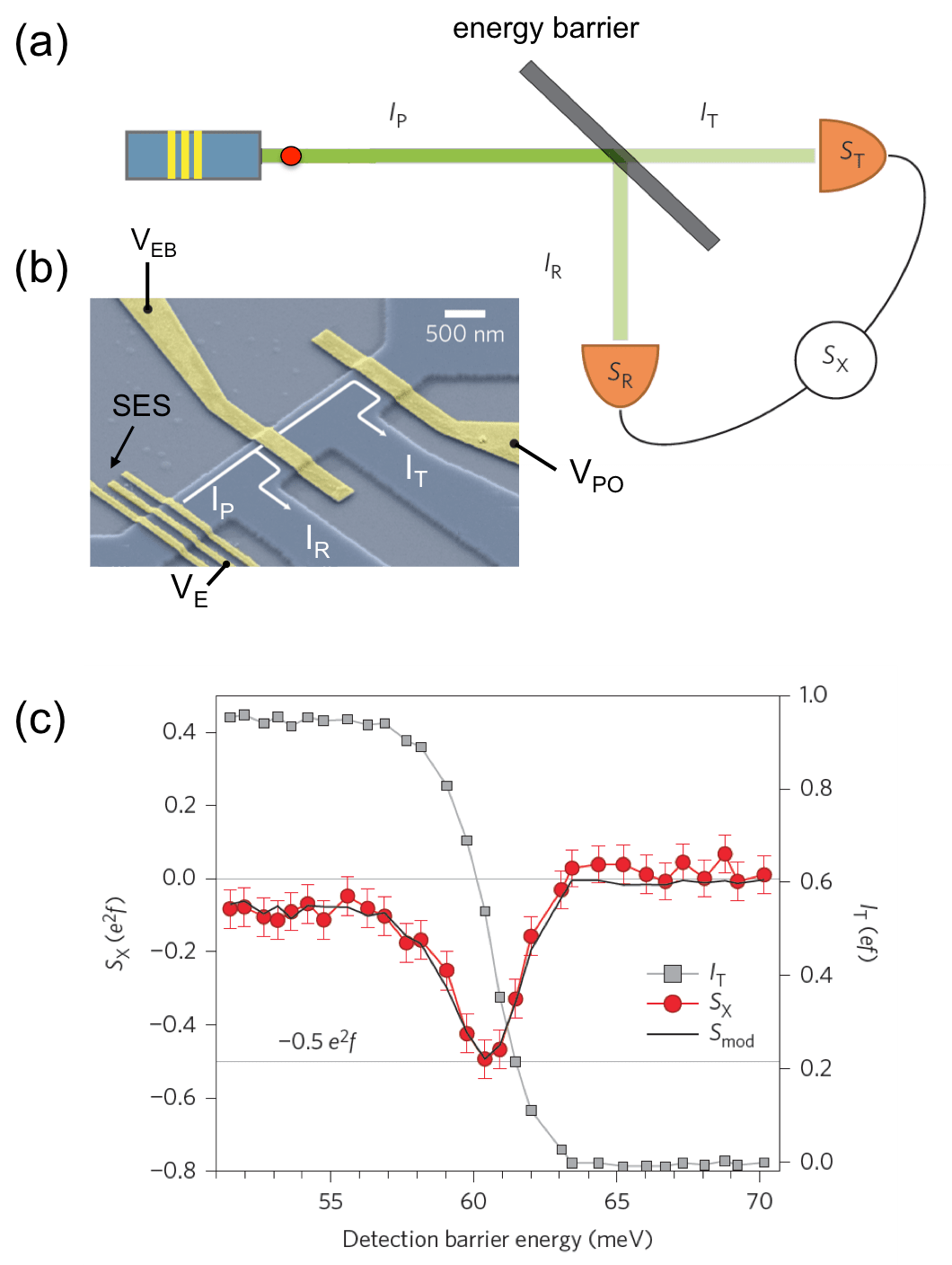
An interesting feature arises when sending electron pairs rather than a single electron. It is possible to load two electrons into the electron pump and emit them within one pumping cycle. When the pump is operated with a sinusoidal drive, the electron are emitted Ubbelohde et al. (2015) sequentially at the same energy since the electron source is operated in the adiabatic limit. The electrons have initially an energy separation due to the charging energy, but due to the slow operation of the pump, the electron has time to compensate the charging energy before emission. Independent scattering will arise at the potential barrier and each of the two emitted electrons will be partitioned with the same transmission probability resulting in the same binomial partitioning distribution, , and . Here corresponds to the probability that (2-) electrons are detected in the transmitted (reflected) current. This is very similar to the single electron emission case. One observes that the current evolves smoothly from an almost perfect transmitted current a low barrier hight towards a fully reflected current at high barrier height, with the appearance of a single dip in the partitioning noise for a transmission probability of . This corresponds to a 50 % probability that the electron pair is partitioned in such a way that they arrive in the opposite outputs. The other 50 % correspond to detecting the two electrons either at output or at output , each event having a probability of 25 %.
The situation is quite different when operating the current source with a short emission pulse rather than a sine wave in order to reduce the time delay between the emission of the two electrons. In this case the charging energy is important and the two electrons cannot be treated as independent any more. They are emitted almost simultaneously, but with different energies. This is seen in the noise correlation measurements which show two distinct dips as a function of barrier hight indicating that the electrons are emitted at different energies. In addition, this is accompanied by a plateau observed for at energies E 52-55 meV. As a consequence, the probability distribution in this energy interval is enhanced, (see figure 22 (d)) reaching a value of 90 %. The barrier therefore acts as an efficient energy filter. Indeed, electrons arriving with different energies are partitioned to different ports and the probability distribution should reach 1 if the energy selection of the barrier were perfect. One also observes a small feature of positive cross-correlation, a small peak in at an energy of 57meV, which means that the electrons show bunching. This feature is presently not understood. It would also be interesting to see whether coherent manipulations of such high energy electrons is possible due to their high energy.
VII Novel quantum interference experiments with short voltage pulses
With the ability to generate very short voltage pulses comes the possibility to probe the quantum dynamics at scales faster than the propagation time through the sample. This is a new direction for quantum nanoelectronics that already has interesting promises, that we illustrate below: the non-adiabatic probing of the quantum dynamics. These non-adiabatic regimes require very fast electronics. Indeed, typical Fermi velocities in a 2DEG are of the order of while the typical system size that can remain coherent is of the order of 10, so that the typical dwell time inside such a ballistic system is 100 . When one uses longer pulses, the propagation inside the sample cannot be probed. In fact, in order to observe the novel interference effect described later in this section, the duration of the pulse must be significantly shorter than 100 as the Coulomb interaction induces a renormalisation of the Fermi velocity into the larger plasmonic velocity Chaplik (1985).
To illustrate the effects that can occur in the non-adiabatic regime, let us focus on numerical simulations of the Mach–Zehnder interferometer of figure 4 in the time domain. A typical snapshot of a simulation is shown in figure 23a: at , one abruptly raises the voltage at contact 0 (, where is the Heavyside function) and studies the propagation of the current front along the two arms of the interferometer. The three snapshots correspond to different times: in the first, the front has reached the first QPC, in the second the front has arrived to contact 1 through the short lower arm, but is still traveling along the upper arm (this is the transient regime on which we focus below), in the third, the front has arrived through both arms and one has reached a stationary state. The corresponding current observed at contact 1 is shown in figure 23b. In the transient regime, one observes a very striking effect: The current oscillates in time with a frequency set by the voltage bias, . This is the mesoscopic analog to the AC Josephson effect in superconducting junctions Gaury et al. (2015). An effect of similar nature can be observed if one replaces the abrupt raise of voltage by short voltage pulses. In a typical experiment, the protocol would be repeated at rather low frequency and one would measure the DC current flowing through contact 1. One finds where is the average number of particle transmitted to contact 1 per pulse. In the ”standard” adiabatic regime (pulses long with respect to the internal time scales of the device), one expects where is the average number of particles sent in the pulse. However, for short pulses, one finds a rather different behavior Gaury and Waintal (2014) with , i.e. the number of electrons collected at contact 1 oscillates with the number of electrons sent.
Let us now build a simple theory that allows one to understand these two effects in a rather simple way. Let us start by considering the propagation of a voltage pulse in a simple one-dimensional wire. The first thing to realise, is that such a voltage pulse cannot be simply associated with the classical propagation of a ballistic excitation as would be the case in vacuum. Indeed, we are considering an electronic system with a Fermi sea, so that before one sends the pulse, the system is not empty; it already sustains stationary plane waves of the form
| (14) |
We now assume that the voltage pulse leads to an abrupt drop of electric potential at (i.e. ). We also suppose, for simplicity, that the voltage is small with respect to the Fermi energy so that one can linearise the dispersion relation . Under this condition, the effect of the increased voltage reduces to a faster oscillation of the wave function phase for which leads to a ”phase domain wall” which propagates ballistically inside the system. The corresponding wave function reads,
| (15) |
where the phase is the total phase accumulated due to the time dependent voltage,
| (16) |
Equation (15) has an interesting structure which was first analysed by Levitov and co workers, in particular in the context of Lorentzian pulses (levitons) and the associated (lack of) quantum noiseKeeling et al. (2006). What is particularly appealing is the fact that the wave function phase is entirely engineered by the physicist through the shape of the voltage pulse, i.e. a quantum object (a wave function phase) is controlled by a classical, experimentally tunable quantity (a voltage). Phases cannot be observed by themselves, so that the next step is to feed this wave function to an electronic interferometer in order to probe this special feature. We focus on the two path interferometer of figure 23a, with an ”upper” and ”lower” arm, described by a transmission amplitude
| (17) |
where the energy dependency is controlled by the delay of propagation of the upper arm with respect to the lower one. For the Mach–Zehnder interferometer of figures 4 and 23a, and (, transmission probability of the corresponding QPC) while for the flying qubit of section figure 8, and . The wave function after the interferometer takes the form (up to a global plane wave phase).
| (18) |
The interesting aspect of Eq.(18) is the fact that the two phases are delayed by the time which enables the possibility to control the interference pattern hence to access the wave function experimentally. Let us discuss a few specific example. In the ”adiabatic” limit where varies very slowly with respect to , and are essentially the same and one is back to the usual DC theory. In the opposite limit, one sends a pulse which is very short with respect to so that abruptly goes from to where is the average number of electrons sent by the pulse, according to the Landauer formula . Let us focus on the wave function somewhere after the interferometer. At both small and large time, one recovers the usual interference pattern,
| (19) |
but in the transient regime where the pulse has arrived through the lower arm but not yet through the upper one, one gets a dynamically modified interference pattern:
| (20) |
which oscillates with the number of particles sent (i.e. with the amplitude of the pulse). This effect is even more drastic if one considers an abrupt raise of potential from to instead of a pulse: . One gets,
| (21) |
The interference pattern in the transient regime now oscillates in time with frequency . This is the normal effect analogous to the ac Josephson effect in superconductors advertised above. To conclude this section, the dynamical control of coherent conductors opens the possibility for a direct manipulation of quantum mechanical objects - the phase of the electronic wavefunction - which gives rise to physical phenomena that have no DC equivalents.
VIII Outlook and future developments
The field of single electron electronics is now at a point where quantum interference experiments at the single-electron level are possible Bocquillon et al. (2013a); Dubois et al. (2013a). As we have seen above, on-chip experiments with individual electrons can now be performed, similar to those realised with single photons on optical tables. When combined with quantum interferometers, these building blocks will form the basis for the next generation of quantum electronic circuits and a multitude of novel experiments not accessible with standard DC voltage sources can be envisioned. For instance when combining single electron voltage pulses with MZ type interferometers, strikingly different behaviours are predicted compared to the static case. Depending on the number of electron charges contained in a voltage pulse the visibility of the current oscillations can be higher than for the static case Hofer and Flindt (2014); Beggi et al. (2015).
An interesting feature of the physics of voltage pulses is that it allows probing quantities which are hardly accessible by other means. One example is the full counting statistics (FCS) of a mesoscopic conductor. When a single charge can be trapped for a relatively long time, such as in quantum dots, single charge detection allowed for measurements of cumulants up to 15th order. For single flying electrons this is presently out of reach. Up to now, only cumulants up to third order have been accessible for mesoscopic conductors Reulet et al. (2003); Bomze et al. (2005); Timofeev et al. (2007). Using a dynamical scheme, however, it has been proposed that by simply measuring the average current, the FCS should be accessible Dasenbrook and Flindt (2016). This can be realised by injecting periodic voltage pulses into a quantum conductor and a MZ interferometer which are capacitively coupled through one arm of the interferometer. The propagating electron wave packet in the quantum conductor will couple to the electron wave packet propagating in one arm of the MZ interferometer and induce an additional phase shift which can be accessed via the average current. By changing the relative time delay between the two electron wave packets, the effective coupling can be controlled and which in turn controls the counting field of the FCS.
The controlled emission of single electron excitations constitutes also an important step forward towards the on-demand generation and detection of entangled single- and few-electron states in mesoscopic structures Hofer et al. (2017). The coherent partitioning at a QPC or tunnel-coupled wire leads to an entanglement between the electron wave functions leaving the two output paths Dasenbrook et al. (2016). Entanglement could then be demonstrated via violation of Bell’s inequality Zhan et al. (2017) by measurements of the mean current and the zero frequency noise.
The ability to generate non-integer charge pulses open another interesting perspective. As mentioned above, for the case of integer charge pulses of Lorentzian shape one can generate a pure electronic excitation Levitov et al. (1996); Dubois et al. (2013a). However, by simply varying the voltage pulse amplitude one can generate any value of the injected charge. In this case the generated excitations Vanević et al. (2007, 2008, 2017) cannot be considered as a pure leviton and interesting new features appear. For instance, for the case of half-levitons, a Lorentzian charge pulse containing half an electron charge, remarkable zero-energy single particle states can be generated Moskalets (2016). The energy distribution function of such a state is symmetric and sharply peaked at the Fermi energy. As a consequence, one can annihilate effectively a half leviton and its anti-particle - an anti-half leviton - which can be created by reversing the sign of the voltage pulse. Such an annihilation effect, not possible with ordinary quasiparticles can then be realised by colliding such anti-particles on a beam splitter. Similarly, when non-integer charge pulses are injected into a MZ interferometer unusual features compared to the static case arise Hofer and Flindt (2014).
Another research line is the study of interactions in one-dimensional electron systems Giamarchi (2003); Deshpande et al. (2010). A typical example are the chiral edge states of the fractional quantum Hall effect (FQHE). The possibility to inject time-resolved wave packets, in particular minimal excitation states by means of levitons, provides a new tool to study the anyonic statistics. This regime has been considered theoretically recently Safi and Sukhorukov (2010); Rech et al. (2017); Ferraro et al. (2017); Ronetti et al. (2017) and the question at present is whether these minimal excitation states can indeed probe the fractional charge excitations. As levitons must carry an integer charge, hence involving several Laughlin quasiparticles, they are believed to leave a signature in the partition noise. A source of fractional charges made of integer charge levitons weakly backscattered by a QPC at FQHE filling factor has been proposed recently Glattli and Roulleau (2017), which may be used to probe anyonic statistics. This on-demand source of anyons would generate a Poissonian flux of charges keeping the time resolved properties of the integer charge levitons. As shown in Fig. 24, synchronizing two anyon sources and sending them to a QPC-beam-splitter should evidence their quantum statistics via HOM correlations or other two particle interferometry Ferraro et al. (2015).
Interactions in one-dimensional electrons systems can also be probed by time of flight measurements. Injecting an electron into a one-dimensional electron system, Coulomb interactions lead to spin-charge separation Auslaender et al. (2005); Jompol et al. (2009) and charge fractionalisation Safi and Schulz (1995, ); Steinberg et al. (2008). This charge fractionalisation as well as the propagation speed of the created charge excitations depend on the strength of the Coulomb interaction Deshpande et al. (2010). In pioneering experiments the speed of such excitations has been measured indirectly from the dispersion relation exploiting a momentum and energy conserving tunnelling process between two quantum wiresAuslaender et al. (2005). Such samples are quite challenging to realise as two two-dimensional electron gas systems have to be brought into close contact to allow tunnelling in between them. More recently this charge fractionalisation has also been investigated in the quantum Hall edge channels Bocquillon et al. (2013b); Inoue et al. (2014); Kamata et al. (2014); Freulon et al. (2015); Hashisaka et al. (2017). A conceptually simpler way to determine the propagation speed of such excitations is to measure directly the time of flight. This however requires an extremely precise control of emission and detection of the injected wave packet. With the development of faster and faster RF electronics this is now possible Kataoka et al. (2016); Hashisaka et al. (2017). It would hence be interesting to see what happens to a leviton when injected into a quantum wire defined by electrostatic gates or into a quantum Hall edge state. Due to Coulomb interaction this initial wave packet should fractionalise Ferraro et al. (2013) and the resulting quasiparticle excitations will propagate with different speeds. For instance for a quantum wire defined by electrostatic gates, it should be possible to access the propagation speed of the individual modes of the quantum wire. One expects that the propagation velocity is strongly renormalised due to Coulomb interactions Matveev and Glazman (1993a, b). This has been experimentally demonstrated very recently G. Roussely et al. (2017).
Finally let us mention that with the development of faster and faster radio-frequency (RF) techniques it should be possible to reach in the near future frequencies that are comparable to the internal characteristic time scales that set the quantum dynamics of the quantum nanoelectronic devices. This field of ultra-fast quantum nanoelectronics is only at its very beginning as voltage pulses of 10 ps or shorter have to be generated. This is highly non-trivial as the generation of such short pulses using standard RF techniques is already challenging from a technological point of view. At present RF technology is limited to the 100 GHz bandwidth. In addition, limits are set due to the dispersive character of the electrical lines, which connect the room temperature microwave electronics with the quantum electronic devices situated at very low temperatures. An alternative approach is to adopt well known techniques from THz optics and make them compatible with nanoelectronic circuits. Sub-picosecond electrical pulses can be generated on chip using photoconductive switches Auston (1975): The photo switch is illuminated by a laser pulse of sub-picosecond duration. The THz field is then confined near a lithographically defined metallic transmission line and converted on-chip into an electrical signal. The width of the generated voltage pulse is limited by the electron hole recombination time which can be as short as 1 ps or even below, depending on the material properties of the photo switches. Several low temperatures transport experiments using this scheme have been carried out in the past Zhong et al. (2008); Wu et al. (2015), however to reach the quantum regime of a nanoelectronic conductor is still a big step away. The challenge here is to develop efficient photo-switches in order to reduce the heat generated by the femto second laser. First attempts have been done in this direction Wood et al. (2013); Hunter et al. (2015) and in future interesting developments can be expected.
From coherent single electron devices we can certainly expect in the future many diverse and fascinating developments. A strong motivation for the field remains to exploit the fermionic nature of the single particle excitations as well as the study of more exotic single particle excitations, such as anyons. With the possibility to combine single electron injection and readout will open the avenue for the realisation of full quantum experiments. It will allow to access the Full Counting Statistics (FCS) of electrons partitioned by a well-controlled interferometer and will bring the field of electron quantum optics to a status similar to that of quantum optics with photons. We expect the emergence of new concepts at the crossroads between quantum optics and solid state nanoelectronics. From the quantum information point of view, new opportunities for linear quantum optics entanglement will emerge that are hardly possible with photons. Concepts such as universal quantum computing with loop based architectures as recently proposed for photonic systems Takeda and Furusawa (2017) might also be more easily accessible in nanoelectronic devices using ultrashort voltage pulses. Promising applications of the single-electron physics are also the possibility to verify very precisely signal shapes on-chip Johnson et al. (2017), which may find applications in the on-chip control of quantum systems.
References
- Kouwenhoven et al. (1997) L. P. Kouwenhoven, C. M. Marcus, P. L. McEuen, S. Tarucha, R. M. Westervelt, and N. S. Wingreen, “Electron Transport in Quantum Dots,” in Mesocopic Electron Transport, edited by L.L. Sohn, L.P. Kouwenhoven, and G. Schön NATO ASI Series, Kluwer Series E vol. 345, 105–214 (1997).
- van der Wiel et al. (2002) W. G. van der Wiel, S. De Franceschi, J. M. Elzerman, T. Fujisawa, S. Tarucha, and L. P. Kouwenhoven, “Electron transport through double quantum dots,” Rev. Mod. Phys. 75, 1–22 (2002).
- Fujisawa et al. (2006) Toshimasa Fujisawa, Toshiaki Hayashi, and Satoshi Sasaki, “Time-dependent single-electron transport through quantum dots,” Reports on Progress in Physics 69, 759–796 (2006).
- De Franceschi et al. (2010) Silvano De Franceschi, Leo Kouwenhoven, Christian Schönenberger, and Wolfgang Wernsdorfer, “Hybrid superconductor–quantum dot devices,” Nature Nanotechnology 5, 703–711 (2010).
- Laird et al. (2015) Edward A. Laird, Ferdinand Kuemmeth, Gary A. Steele, Kasper Grove-Rasmussen, Jesper Nygård, Karsten Flensberg, and Leo P. Kouwenhoven, “Quantum transport in carbon nanotubes,” Rev. Mod. Phys. 87, 703–764 (2015).
- Bertoni et al. (2000) A. Bertoni, P. Bordone, R. Brunetti, C. Jacoboni, and S. Reggiani, “Quantum Logic Gates based on Coherent Electron Transport in Quantum Wires,” Phys. Rev. Lett. 84, 5912 (2000).
- Ionicioiu et al. (2001a) Radu Ionicioiu, Gehan Amaratunga, and Florin Udrea, “Quantum Computation with ballistic electrons,” International Journal of Modern Physics B 15, 125–133 (2001a).
- Barnes et al. (2000) C. H. W. Barnes, J. M. Shilton, and A. M. Robinson, “Quantum computation using electrons trapped by surface acoustic waves,” Phys. Rev. B 62, 8410–8419 (2000).
- Beenakker et al. (2004) C. W. J. Beenakker, D. P. DiVincenzo, C. Emary, and M. Kindermann, “Charge detection enables free-electron quantum computation,” Phys. Rev. Lett. 93, 020501 (2004).
- Bertrand et al. (2016a) B. Bertrand, S. Hermelin, S. Takada, M. Yamamoto, S. Tarucha, A. Ludwig, A. D. Wieck, C. Bäuerle, and T. Meunier, “Fast spin information transfer between distant quantum dots using individual electrons,” Nature Nanotechnology 11, 672–676 (2016a).
- DiVincenzo (2000) D. P. DiVincenzo, “The Physical Implementation of Quantum Computation,” Fortschr. Phys. 48, 771–783 (2000).
- Fowler et al. (2012) Austin G. Fowler, Matteo Mariantoni, John M. Martinis, and Andrew N. Cleland, “Surface codes: Towards practical large-scale quantum computation,” Phys. Rev. A 86, 032324 (2012).
- Hanson et al. (2007) R. Hanson, L. P. Kouwenhoven, J. R. Petta, S. Tarucha, and L. M. K. Vandersypen, “Spins in few-electron quantum dots,” Rev. Mod. Phys. 79, 1217–1265 (2007).
- Zwanenburg et al. (2013) Floris A. Zwanenburg, Andrew S. Dzurak, Andrea Morello, Michelle Y. Simmons, Lloyd C. L. Hollenberg, Gerhard Klimeck, Sven Rogge, Susan N. Coppersmith, and Mark A. Eriksson, “Silicon quantum electronics,” Rev. Mod. Phys. 85, 961–1019 (2013).
- Awschalom et al. (2013) D. D. Awschalom, L. C. Bassett, A. S. Dzurak, E. L. Hu, and J. R. Petta, “Quantum Spintronics: Engineering and Manipulating Atom-Like Spins in Semiconductors,” Science 339, 1174–1179 (2013).
- Flentje et al. (2017) H. Flentje, P.-A. Mortemousque, R. Thalineau, A. Ludwig, A. D. Wieck, C. Bäuerle, and T. Meunier, “Coherent long-distance displacement of individual electron spins,” Nature Communications 8, 501 (2017).
- Fujita et al. (2017) Takafumi Fujita, Timothy Alexander Baart, Christian Reichl, Werner Wegscheider, and Lieven Mark Koenraad Vandersypen, “Coherent shuttle of electron-spin states,” npj Quantum Information 3, 22 (2017).
- Wallraff et al. (2004) A. Wallraff, D. I. Schuster, A. Blais, L. Frunzio, R. S. Huang, J. Majer, S. Kumar, S. M. Girvin, and R. J. Schoelkopf, “Strong coupling of a single photon to a superconducting qubit using circuit quantum electrodynamics,” Nature 431, 162–167 (2004).
- Houck et al. (2007) A. A. Houck, D. I. Schuster, J. M. Gambetta, J. A. Schreier, B. R. Johnson, J. M. Chow, L. Frunzio, J. Majer, M. H. Devoret, S. M. Girvin, and R. J. Schoelkopf, “Generating single microwave photons in a circuit,” Nature 449, 328–331 (2007).
- Roch et al. (2014) N. Roch, M. E. Schwartz, F. Motzoi, C. Macklin, R. Vijay, A. W. Eddins, A. N. Korotkov, K. B. Whaley, M. Sarovar, and I. Siddiqi, “Observation of Measurement-Induced Entanglement and Quantum Trajectories of Remote Superconducting Qubits,” Phys. Rev. Lett. 112, 170501 (2014).
- Nielsen and Chuang (2000) M. A. Nielsen and I. L. Chuang, Quantum Computation and Quantum Information (Cambridge University Press, Cambridge, England, 2000).
- Barenco et al. (1995) Adriano Barenco, Charles H. Bennett, Richard Cleve, David P. DiVincenzo, Norman Margolus, Peter Shor, Tycho Sleator, John A. Smolin, and Harald Weinfurter, “Elementary gates for quantum computation,” Phys. Rev. A 52, 3457–3467 (1995).
- del Alamo and Eugster (1990) Jesús A. del Alamo and Cristopher C. Eugster, “Quantum field‐effect directional coupler,” Applied Physics Letters 56, 78–80 (1990).
- Tsukada et al. (1990) N. Tsukada, A. D. Wieck, and K. Ploog, “Proposal of novel electron wave coupled devices,” Applied Physics Letters 56, 2527–2529 (1990).
- Xu et al. (1993) Guangzhao Xu, Min Yang, and Ping Jiang, “A theoratical investigation on the quantum field effect directional coupler,” Journal of Applied Physics 74, 6747–6753 (1993).
- Bautze et al. (2014) Tobias Bautze, Christoph Süssmeier, Shintaro Takada, Christoph Groth, Tristan Meunier, Michihisa Yamamoto, Seigo Tarucha, Xavier Waintal, and Christopher Bäuerle, “Theoretical, numerical, and experimental study of a flying qubit electronic interferometer,” Phys. Rev. B 89, 125432 (2014).
- Gaury et al. (2014) Benoit Gaury, Joseph Weston, Matthieu Santin, Manuel Houzet, Christoph Groth, and Xavier Waintal, “Numerical simulations of time-resolved quantum electronics,” Physics Reports 534, 1–37 (2014).
- Aharonov and Bohm (1959) Y. Aharonov and D. Bohm, “Significance of Electromagnetic Potentials in the Quantum Theory,” Physical Review 115, 485–491 (1959).
- Tonomura and Batelaan (2009) Akira Tonomura and Herman Batelaan, “The Aharonov–Bohm effects: Variations on a subtle theme,” Physics Today 62, 38–43 (2009).
- Yamamoto et al. (2012) Michihisa Yamamoto, Shintaro Takada, Christopher Bäuerle, Kenta Watanabe, Andreas D. Wieck, and Seigo Tarucha, “Electrical control of a solid-state flying qubit,” Nature Nanotechnology 7, 247–251 (2012).
- Yu and Voskoboynikov (2008) Leo Yu and Oleksandr Voskoboynikov, “Ballistic Aharonov – Bohm quantum bits and quantum gates,” Solid State Communications 145, 447–450 (2008).
- Schomerus and Robinson (2007) Henning Schomerus and John P. Robinson, “Entanglement between static and flying qubits in an Aharonov–Bohm double electrometer,” New Journal of Physics 9, 67 (2007).
- Buscemi et al. (2012) Fabrizio Buscemi, Paolo Bordone, and Andrea Bertoni, “Electron interference and entanglement in coupled 1D systems with noise,” The European Physical Journal D 66, 312 (2012).
- Ionicioiu et al. (2001b) Radu Ionicioiu, Paolo Zanardi, and Fausto Rossi, “Testing Bell’s inequality with ballistic electrons in semiconductors,” Phys. Rev. A 63, 050101(R) (2001b).
- Knill et al. (2001) Emanuel Knill, R. Laflamme, and G. J. Milburn, “A scheme for efficient quantum computation with linear optics.” Nature 409, 46–52 (2001).
- O’Brien et al. (2003) J. L. O’Brien, G. J. Pryde, A. G. White, T. C. Ralph, and D. Branning, “Demonstration of an all-optical quantum controlled-NOT gate,” Nature 426, 264–267 (2003).
- Politi et al. (2008) Alberto Politi, Martin J. Cryan, John G. Rarity, Siyuan Yu, and Jeremy L. O’Brien, “Silica-on-silicon waveguide quantum circuits,” Science 320, 646–649 (2008).
- Carolan et al. (2015) Jacques Carolan, Christopher Harrold, Chris Sparrow, Enrique Martín-lópez, Nicholas J. Russell, Joshua W. Silverstone, Peter J. Shadbolt, Nobuyuki Matsuda, Manabu Oguma, Mikitaka Itoh, Graham D. Marshall, Mark G. Thompson, Jonathan C. F. Matthews, Toshikazu Hashimoto, Jeremy L. O’Brien, and Anthony Laing, “Universal linear optics,” Science 349, 711 (2015).
- Roulleau et al. (2008a) Preden Roulleau, F. Portier, P. Roche, A. Cavanna, G. Faini, U. Gennser, and D. Mailly, “Direct Measurement of the Coherence Length of Edge States in the Integer Quantum Hall Regime,” Phys. Rev. Lett. 100, 126802 (2008a).
- Niimi et al. (2009) Y. Niimi, Y. Baines, T. Capron, D. Mailly, F. Y. Lo, A. D. Wieck, T. Meunier, L. Saminadayar, and C. Bäuerle, “Effect of Disorder on the Quantum Coherence in Mesoscopic Wires,” Phys. Rev. Lett. 102, 226801 (2009).
- Niimi et al. (2010) Yasuhiro Niimi, Yannick Baines, Thibaut Capron, Dominique Mailly, Fang Yuh Lo, Andreas D. Wieck, Tristan Meunier, Laurent Saminadayar, and Christopher Bäuerle, “Quantum coherence at low temperatures in mesoscopic systems: Effect of disorder,” Phy. Rev. B 81, 245306 (2010).
- Jönsson (1961) Claus Jönsson, “Elektroneninterferenzen an mehreren knstlich hergestellten feinspalten,” Z. Physik 161, 454 (1961).
- Tonomura et al. (1989) A. Tonomura, J. Endo, T. Matsuda, T. Kawasaki, and H. Ezawa, “Demonstration of single-electron buildup of an interference pattern,” Amer. J. Phys. 57, 117 (1989).
- Young (1804) T. Young, “The bakerian lecture. experiments and calculations relative to physical optics,” Phil. Trans. R. Soc. Lond. 94, 1–16 (1804).
- Hecht (1974) Eugene Hecht, Optics (Addison-Wesely Publishing Company, 1974).
- Webb et al. (1985) R. A. Webb, S. Washburn, C. P. Umbach, and R. B. Laibowitz, “Observation of Aharonov-Bohm Oscillations in Normal-Metal Rings,” Phys. Rev. Lett. 54, 2696–2699 (1985).
- Chandrasekhar et al. (1985) V. Chandrasekhar, M. J. Rooks, S. Wind, and D. E. Prober, “Observation of Aharonov-Bohm Electron Interference Effects with Periods and in Individual Micron-Size, Normal-Metal Rings,” Phys. Rev. Lett. 55, 1610–1613 (1985).
- Washburn and Webb (1986) Sean Washburn and Richard A. Webb, “Aharonov-Bohm effect in normal metal quantum coherence and transport,” Advances in Physics 35, 375–422 (1986).
- Yacoby et al. (1995) A Yacoby, M Heiblum, D Mahalu, and Hadas Shtrikman, “Coherence and Phase Sensitive Measurements in a Quantum Dot,” Phys. Rev. Lett. 74, 4047–4050 (1995).
- Buks et al. (1998) E. Buks, R. Schuster, M. Heiblum, D. Mahalu, and V. Umansky, “Dephasing in electron interference by a ‘which-path’ detector,” Nature 391, 871–874 (1998).
- Gustavsson et al. (2008) S. Gustavsson, R. Leturcq, M. Studer, T. Ihn, K. Ensslin, D. C. Driscoll, and A. C. Gossard, “Time-resolved detection of single-electron interference,” Nano Letters 8, 2547–2550 (2008).
- Note (1) More precisely, the electron couples to the vector potential Aharonov and Bohm (1959) rather than the magnetic field, hence even if the electron does not experience a magnetic field, for instance when passing next to an infinite solenoidal coil, the electron picks up a phase (see also ref. Tonomura and Batelaan (2009)).
- Büttiker et al. (1985) M. Büttiker, Y. Imry, R. Landauer, and S. Pinhas, “Generalized many-channel conductance formula with application to small rings,” Phys. Rev. B 31, 6207–6215 (1985).
- Yeyati and Büttiker (1995) A. Levy Yeyati and M. Büttiker, “Aharonov-Bohm oscillations in a mesoscopic ring with a quantum dot,” Phys. Rev. B 52, R14360–R14363 (1995).
- Yacoby et al. (1996) A. Yacoby, R. Schuster, and M. Heiblum, “Phase rigidity and h/2e oscillations in a single-ring Aharonov-Bohm experiment,” Phys. Rev. B 53, 9583–9586 (1996).
- van Wees et al. (1988) B. J. van Wees, H. Van Houten, C. W. J. Beenakker, J. G. Williamson, L. P. Kouwenhoven, D. Van Der Marel, and C. T. Foxon, “Quantized conductance of point contacts in a two-dimensional electron gas,” Phys. Rev. Lett. 60, 848–850 (1988).
- Wharam et al. (1988) D. A. Wharam, T. J. Thornton, R. Newbury, M. Pepper, H. Ahmed, J. E. F. Frost, D. G. Hasko, D. C. Peacock, D. A. Ritchie, and G. A. C. Jones, “One-dimensional transport and the quantisation of the ballistic resistance,” Journal of Physics C: Solid State Physics 21, L209 (1988).
- Ji et al. (2003) Yang Ji, Yunchul Chung, D. Sprinzak, M. Heiblum, D. Mahalu, and Hadas Shtrikman, “An electronic Mach–Zehnder interferometer,” Nature 422, 415–418 (2003).
- Litvin et al. (2008) L. V. Litvin, A. Helzel, H. P. Tranitz, W. Wegscheider, and C. Strunk, “Edge-channel interference controlled by Landau level filling,” Phys. Rev. B 78, 075303–075304 (2008).
- Huynh et al. (2012) P. A. Huynh, F. Portier, H. Le Sueur, G. Faini, U. Gennser, D. Mailly, F. Pierre, W. Wegscheider, and P. Roche, “Quantum Coherence Engineering in the Integer Quantum Hall Regime,” Phys. Rev. Lett. 108, 256802 (2012).
- Neder et al. (2007a) I. Neder, M. Heiblum, D. Mahalu, and V. Umansky, “Entanglement, dephasing, and phase recovery via cross-correlation measurements of electrons,” Phys. Rev. Lett. 98, 036803 (2007a).
- Neder et al. (2007b) I. Neder, N. Ofek, Y. Chung, M. Heiblum, D. Mahalu, and V. Umansky, “Interference between two indistinguishable electrons from independent sources.” Nature 448, 333–337 (2007b).
- Debray et al. (2001) P. Debray, V. Zverev, O. Raichev, R. Klesse, P. Vasilopoulos, and R. S. Newrock, “Experimental studies of Coulomb drag between ballistic quantum wires,” Journal of Physics: Condensed Matter 13, 3389 (2001).
- Yamamoto et al. (2006) M Yamamoto, M Stopa, Y Tokura, Y Hirayama, and S Tarucha, “Negative Coulomb Drag in a One-Dimensional Wire,” Science 313, 204–207 (2006).
- Laroche et al. (2014) D. Laroche, G. Gervais, M. P. Lilly, and J. L. Reno, “1d-1d coulomb drag signature of a luttinger liquid,” Science 343, 631–634 (2014).
- Neder et al. (2006) I. Neder, M. Heiblum, Y. Levinson, D. Mahalu, and V. Umansky, “Unexpected Behavior in a Two-Path Electron Interferometer,” Phys. Rev. Lett. 96, 016804 (2006).
- Roulleau et al. (2007) Preden Roulleau, F. Portier, D. C. Glattli, P. Roche, A. Cavanna, G. Faini, U. Gennser, and D. Mailly, “Finite bias visibility of the electronic Mach-Zehnder interferometer,” Phys. Rev. B 76, 161309(R) (2007).
- Samuelsson et al. (2004) P. Samuelsson, E. V. Sukhorukov, and M. Büttiker, “Two-particle Aharonov-Bohm effect and entanglement in the electronic Hanbury Brown-Twiss setup.” Phys. Rev. Lett. 92, 026805 (2004).
- Levkivskyi and Sukhorukov (2008) Ivan P. Levkivskyi and Eugene V. Sukhorukov, “Dephasing in the electronic Mach-Zehnder interferometer at filling factor =2,” Phys. Rev. B 78, 045322 (2008).
- Roulleau et al. (2008b) P. Roulleau, F. Portier, P. Roche, A. Cavanna, G. Faini, U. Gennser, and D. Mailly, “Noise Dephasing in Edge States of the Integer Quantum Hall Regime,” Phys. Rev. Lett. 101, 186803 (2008b).
- Bocquillon et al. (2013a) E. Bocquillon, V. Freulon, J. M. Berroir, P. Degiovanni, B. Plaçais, A. Cavanna, Y. Jin, and G. Fève, “Coherence and Indistinguishability of Single Electrons Emitted by Independent Sources,” Scienc 339, 1054–1057 (2013a).
- Lee and Eric Yang (1997) H. C. Lee and S. R. Eric Yang, “Spin-charge separation in quantum Hall edge liquids,” Phys. Rev. B 56, R15529–R15532 (1997).
- Sukhorukov and Cheianov (2007) Eugene V. Sukhorukov and Vadim V. Cheianov, “Resonant Dephasing in the Electronic Mach-Zehnder Interferometer,” Phys. Rev. Lett. 99, 156801 (2007).
- Berg et al. (2009) E. Berg, Y. Oreg, E. A. Kim, and F. von Oppen, “Fractional Charges on an Integer Quantum Hall Edge,” Phys. Rev. Lett. 102, 236402 (2009).
- Levkivskyi and Sukhorukov (2012) Ivan P. Levkivskyi and Eugene V. Sukhorukov, “Energy relaxation at quantum Hall edge,” Phys. Rev. B 85, 075309 (2012).
- Bocquillon et al. (2013b) E. Bocquillon, V. Freulon, J. M. Berroir, P. Degiovanni, B. Plaçais, A. Cavanna, Y. Jin, and G. Fève, “Separation of neutral and charge modes in one-dimensional chiral edge channels.” Nature Communications 4, 1839 (2013b).
- Inoue et al. (2014) H. Inoue, A. Grivnin, N. Ofek, I. Neder, M. Heiblum, V. Umansky, and D. Mahalu, “ Charge fractionalization in the integer quantum hall effect,” Phys. Rev. Lett. 112, 166801 (2014).
- Kamata et al. (2014) H. Kamata, N. Kumada, M. Hashisaka, K. Muraki, and T. Fujisawa, “Fractionalized wave packets from an artificial Tomonaga-Luttinger liquid,” Nature Nanotechnology 9, 177–181 (2014).
- Freulon et al. (2015) V. Freulon, A. Marguerite, J. M. Berroir, B. Plaçais, A. Cavanna, Y. Jin, and G. Fève, “Hong-Ou-Mandel experiment for temporal investigation of single-electron fractionalization,” Nature Communications 6, 6854 (2015).
- Hashisaka et al. (2017) M. Hashisaka, N. Hiyama, T. Akiho, K. Muraki, and T. Fujisawa, “Waveform measurement of charge- and spin-density wavepackets in a chiral Tomonaga–Luttinger liquid,” Nature Physics 13, 559–562 (2017).
- Samuelsson et al. (2009) P. Samuelsson, I. Neder, and M. Büttiker, “Entanglement at finite temperatures in the electronic two-particle interferometer,” Physica Scripta T137, 014023 (2009).
- Samuelsson et al. (2003) P. Samuelsson, E. V. Sukhorukov, and M. Büttiker, “Orbital Entanglement and Violation of Bell Inequalities in Mesoscopic Conductors,” Phys. Rev. Lett. 91, 157002 (2003).
- Samuelsson and Büttiker (2005) P. Samuelsson and M. Büttiker, “Dynamic generation of orbital quasiparticle entanglement in mesoscopic conductors,” Phys. Rev. B 71, 245317 (2005).
- Beenakker et al. (2005) C. W. J. Beenakker, M. Titov, and B. Trauzettel, “Optimal spin-entangled electron-hole pair pump,” Phys. Rev. Lett. 94, 186804 (2005).
- Bell (1966) J. S. Bell, “On the Problem of Hidden Variables in Quantum Mechanics,” Rev. Mod. Phys. 38, 447–452 (1966).
- Edlbauer et al. (2017) H. Edlbauer, S. Takada, G. Roussely, M. Yamamoto, S. Tarucha, A. Ludwig, A. D. Wieck, T. Meunier, and C. Bäuerle, “Non-universal transmission phase behaviour of a large quantum dot,” Nature Communications 8, 1710 (2017).
- Onsager (1931) Lars Onsager, “Reciprocal Relations in Irreversible Processes. I.” Phys. Rev. 37, 405–426 (1931).
- Aharony et al. (2014) A. Aharony, S. Takada, O. Entin-Wohlman, M. Yamamoto, and S. Tarucha, “Aharonov-Bohm interferometry with a tunnel-coupled wire,” New Journal of Physics 16, 083015 (2014).
- Schuster et al. (1997) R. Schuster, E. Buks, M. Heiblum, D. Mahalu, V. Umansky, and Hadas Shtrikman, “Phase measurement in a quantum dot via a double-slit interference experiment,” Nature 385, 417–420 (1997).
- Ji et al. (2000) Yang Ji, M Heiblum, D Sprinzak, D Mahalu, and Hadas Shtrikman, “Phase evolution in a kondo-correlated system,” Science 290, 779–783 (2000).
- Takada et al. (2014) S. Takada, C. Bäuerle, M. Yamamoto, K. Watanabe, S. Hermelin, T. Meunier, A. Alex, A. Weichselbaum, J. von Delft, A. Ludwig, A. D. Wieck, and S. Tarucha, “Transmission Phase in the Kondo Regime Revealed in a Two-Path Interferometer,” Phys. Rev. Lett. 113, 126601 (2014).
- Gregoire (2016) Roussely Gregoire, “PhD thesis: Time resolved measurements in a mesoscopic conductor.” https://tel.archives-ouvertes.fr/tel-01453263 (2016).
- Seelig and Büttiker (2001) Georg Seelig and Markus Büttiker, “Charge-fluctuation-induced dephasing in a gated mesoscopic interferometer,” Phys. Rev. B 64, 245313 (2001).
- Blumenthal et al. (2007) M. D. Blumenthal, B. Kaestner, L. Li, S. Giblin, T. J. B. M. Janssen, M. Pepper, D. Anderson, G. Jones, and D. A. Ritchie, “Gigahertz quantized charge pumping,” Nature Physics 3, 343–347 (2007).
- Fève et al. (2007) G. Fève, A. Mahé , J. M. Berroir, T. Kontos, B. Plaçais, D. C. Glattli, A. Cavanna, B. Etienne, and Y. Jin, “An On-Demand Coherent Single-Electron Source,” Science 316, 1169–1172 (2007).
- Hermelin et al. (2011) Sylvain Hermelin, Shintaro Takada, Michihisa Yamamoto, Seigo Tarucha, Andreas D. Wieck, Laurent Saminadayar, Christopher Bäuerle, and Tristan Meunier, “Electrons surfing on a sound wave as a platforms for quantum optics with flying electrons,” Nature 477, 435–438 (2011).
- Dubois et al. (2013a) J. Dubois, T. Jullien, F. Portier, P. Roche, A. Cavanna, Y. Jin, W. Wegscheider, P. Roulleau, and D. C. Glattli, “Minimal-excitation states for electron quantum optics using levitons,” Nature 502, 659–663 (2013a).
- McNeil et al. (2011) R. P. G. McNeil, M. Kataoka, C. J. B. Ford, C. H. W. Barnes, D. Anderson, G. A. C. Jones, I. Farrer, and D. A. Ritchie, “On-demand single-electron transfer between distant quantum dots,” Nature 477, 439–442 (2011).
- Hermelin et al. (2017) Sylvain Hermelin, Benoit Bertrand, Shintaro Takada, Michihisa Yamamoto, Seigo Tarucha, Arne Ludwig, Andreas D. Wieck, Christopher Bäuerle, and Tristan Meunier, “Classical information transfer between distant quantum dots using individual electrons in fast moving quantum dots,” Phys. Status Solidi B 254, 1600673 (2017).
- Ford (2017) Christopher J.B. Ford, “Transporting and manipulating single electrons in surface-acoustic-wave minima,” Phys. Status Solidi B 254, 1600658 (2017).
- Haack et al. (2011) Géraldine Haack, Michael Moskalets, Janine Splettstoesser, and Markus Büttiker, “Coherence of single-electron sources from Mach-Zehnder interferometry ,” Phys. Rev. B 84, 081303(R) (2011).
- Rosselló et al. (2015) Guillem Rosselló, Francesca Battista, Michael Moskalets, and Janine Splettstoesser, “Interference and multiparticle effects in a Mach-Zehnder interferometer with single-particle sources,” Phys. Rev. B 91, 115438 (2015).
- Gaury and Waintal (2014) Benoit Gaury and Xavier Waintal, “Dynamical control of interference using voltage pulses in the quantum regime,” Nature Communications 5, 3844 (2014).
- Pekola et al. (2013) Jukka P. Pekola, Olli-Pentti Saira, Ville F. Maisi, Antti Kemppinen, Mikko Möttönen, Yuri A. Pashkin, and Dmitri V. Averin, “Single-electron current sources: Toward a refined definition of the ampere,” Rev. of Mod. Phys. 85, 1421–1472 (2013).
- Kaestner and Kashcheyevs (2015) Bernd Kaestner and Vyacheslavs Kashcheyevs, “Non-adiabatic quantized charge pumping with tunable-barrier quantum dots: a review of current progress,” Reports on Progress in Physics 78, 103901 (2015).
- Kaneko et al. (2016) Nobu-Hisa Kaneko, Shuji Nakamura, and Yuma Okazaki, “A review of the quantum current standard,” Measurement Science and Technology 27, 032001 (2016).
- des Poids et Mesures) (2010) BIPM (Bureau International des Poids et Mesures), “The future SI,” [https://tel.archives-ouvertes.fr/tel-00721761] (2010).
- Mills et al. (2011) I. M. Mills, P. J. Mohr, T. J. Quinn, B. N. Taylor, and E. R. Williams, “Adapting the International System of Units to the twenty-first century,” Phil. Trans. R. Soc. A 369, 3907–3924 (2011).
- Gibney (2017) Elizabeth Gibney, “New definitions of scientific units are on the horizon,” Nature 550, 312 (2017).
- Keller (2008) Mark W. Keller, “Current status of the quantum metrology triangle,” Metrologia 45, 102 (2008).
- Feltin and Piquemal (2009) N. Feltin and F. Piquemal, “Determination of the elementary charge and the quantum metrological triangle experiment,” Euro. Phys. J. Special Topics 172, 267–296 (2009).
- Yamahata et al. (2016) Gento Yamahata, Stephen P. Giblin, Masaya Kataoka, Takeshi Karasawa, and Akira Fujiwara, “Gigahertz single-electron pumping in silicon with an accuracy better than 9.2 parts in ,” Applied Physics Letters 109, 013101 (2016).
- Stein et al. (2017) F Stein, H. Scherer, T. Gerster, R. Behr, M. Götz, E. Pesel, C. Leicht, N. Ubbelohde, T. Weimann, K. Pierz, H. W. Schumacher, and F. Hohls, “Robustness of single-electron pumps at sub-ppm current accuracy level,” Metrologia 54, S1 (2017).
- Zhao et al. (2017) R. Zhao, A. Rossi, S. P. Giblin, J. D. Fletcher, F. E. Hudson, M. Möttöonen, M. Kataoka, and A. S. Dzurak, “Thermal-error regime in high-accuracy gigahertz single-electron pumping,” Phys. Rev. Applied 8, 044021 (2017).
- Kastner (1992) M. A. Kastner, “The single-electron transistor,” Rev. Mod. Phys. 64, 849–858 (1992).
- Reimann and Manninen (2002) Stephanie M. Reimann and Matti Manninen, “Electronic structure of quantum dots,” Rev. Mod. Phys. 74, 1283–1342 (2002).
- Gabelli et al. (2006) J. Gabelli, Gwendal Fève, J. M. Berroir, B. Plaçais, A. Cavanna, B. Etienne, Y. Jin, and D. C. Glattli, “Violation of Kirchhoff’s Laws for a Coherent RC Circuit,” Science 313, 499–502 (2006).
- Büttiker (1993) M. Büttiker, “Mesoscopic Capacitor,” Phys. Lett. A 180, 364–369 (1993).
- Kaestner et al. (2008a) B. Kaestner, V. Kashcheyevs, S. Amakawa, M. D. Blumenthal, L. Li, T. J. B. M. Janssen, G. Hein, K. Pierz, T. Weimann, U. Siegner, and H. W. Schumacher, “Single-parameter nonadiabatic quantized charge pumping,” Phys. Rev. B 77, 153301 (2008a).
- Fujiwara et al. (2008) Akira Fujiwara, Katsuhiko Nishiguchi, and Yukinori Ono, “Nanoampere charge pump by single-electron ratchet using silicon nanowire metal-oxide-semiconductor field-effect transistor,” Applied Physics Letters 92, 042102 (2008).
- Kaestner et al. (2008b) B. Kaestner, V. Kashcheyevs, G. Hein, K. Pierz, U. Siegner, and H. W. Schumacher, “Robust single-parameter quantized charge pumping,” Applied Physics Letters 92, 192106 (2008b).
- Fletcher et al. (2012) J. D. Fletcher, M. Kataoka, S. P. Giblin, Sunghun Park, H. S. Sim, P. See, D. A. Ritchie, J. P. Griffiths, G. A. C. Jones, H. E. Beere, and T. J. B. M. Janssen, “Stabilization of single-electron pumps by high magnetic fields,” Phys. Rev. B 86, 155311 (2012).
- Giblin et al. (2012) S.P. Giblin, M. Kataoka, P. Fletcher, J.D. See, T.J.B.M. Janssen, J.P. Griffiths, G.A.C. Jones, I. Farrer, and D.A. Ritchie, “Towards a quantum representation of the ampere using single electron pumps,” Nature Communications 3, 930 (2012).
- Leicht et al. (2011) C Leicht, P. Mirovsky, B. Kaestner, F. Hohls, V. Kashcheyevs, E. V. Kurganova, U. Zeitler, T. Weimann, K. Pierz, and H. W. Schumacher, “Generation of energy selective excitations in quantum hall edge states,” Semiconductor Science and Technology 26, 055010 (2011).
- Fletcher et al. (2013) J. D. Fletcher, P. See, H. Howe, M. Pepper, S. P. Giblin, J. P. Griffiths, G. A. C. Jones, I. Farrer, D. A. Ritchie, T. J. B. M. Janssen, and M. Kataoka, “Clock-Controlled Emission of Single-Electron Wave Packets in a Solid-State Circuit,” Phys. Rev. Lett. 111, 216807 (2013).
- Waldie et al. (2015) J. Waldie, P. See, V. Kashcheyevs, J. P. Griffiths, I. Farrer, G. A. C. Jones, D. A. Ritchie, T. J. B. M. Janssen, and M. Kataoka, “Measurement and control of electron wave packets from a single-electron source,” Phys. Rev. B 92, 125305 (2015).
- Johnson et al. (2017) N. Johnson, J. D. Fletcher, D. A. Humphreys, P. See, J. P. Griffiths, G. A. C. Jones, I. Farrer, D. A. Ritchie, M. Pepper, T. J. B. M. Janssen, and M. Kataoka, “Ultrafast Voltage Sampling using Single-Electron Wavepackets,” Applied Phys. Lett. 110, 102105 (2017).
- Ubbelohde et al. (2015) Niels Ubbelohde, Frank Hohls, Vyacheslavs Kashcheyevs, Timo Wagner, Lukas Fricke, Bernd Kästner, Klaus Pierz, Hans W. Schumacher, and Rolf J. Haug, “Partitioning of on-demand electron pairs,” Nature Nanotechnology 10, 46–49 (2015).
- Takahashi et al. (2002) Yasuo Takahashi, Yukinori Ono, Akira Fujiwara, and Hiroshi Inokawa, “Silicon single-electron devices,” J. Phys.: Condens. Matter 14, R995––R1033 (2002).
- Mi et al. (2017) X. Mi, J. V. Cady, D. M. Zajac, P. W. Deelman, and J. R. Petta, “Strong coupling of a single electron in silicon to a microwave photon,” Science 355, 156–158 (2017).
- M. et al. (2014) Veldhorst M., Hwang J. C. C., Yang C. H., Leenstra A. W., de Ronde B., Dehollain J. P., Muhonen J. T., Hudson F. E., Itoh K. M., Morello A., and Dzurak A. S., “An addressable quantum dot qubit with fault-tolerant control-fidelity,” Nature Nanotechnology 9, 981–985 (2014).
- Maurand et al. (2016) R. Maurand, X. Jehl, D. Kotekar-Patil, A. Corna, H. Bohuslavskyi, R. Laviéville, L. Hutin, S. Barraud, M. Vinet, M. Sanquer, and S. De Franceschi, “A CMOS silicon spin qubit,” Nature Communications 7, 13575 (2016).
- Muhonen et al. (2014) Juha T. Muhonen, Juan P. Dehollain, Arne Laucht, Fay E. Hudson, Rachpon Kalra, Takeharu Sekiguchi, Kohei M. Itoh, David N. Jamieson, Jeffrey C. McCallum, Andrew S. Dzurak, and Andrea Morello, “Storing quantum information for 30 seconds in a nanoelectronic device,” Nature Nanotechnology 9, 986–991 (2014).
- Levitov et al. (1996) Leonid S. Levitov, Hyunwoo Lee, and Gordey B. Lesovik, “Electron counting statistics and coherent states of electric current,” Journal of Mathematical Physics 37, 4845–4866 (1996).
- Ivanov et al. (1997) D. A. Ivanov, H. W. Lee, and L. S. Levitov, “Coherent states of alternating current,” Phys. Rev. B 56, 6839–6850 (1997).
- Keeling et al. (2006) J. Keeling, I. Klich, and L. S. Levitov, “Minimal Excitation States of Electrons in One-Dimensional Wires,” Phys. Rev. Lett. 97, 116403 (2006).
- Vanević et al. (2007) Mihajlo Vanević, Yuli V. Nazarov, and Wolfgang Belzig, “Elementary events of electron transfer in a voltage-driven quantum point contact,” Phys. Rev. Lett. 99, 076601 (2007).
- Vanević et al. (2008) Mihajlo Vanević, Yuli V. Nazarov, and Wolfgang Belzig, “Elementary charge-transfer processes in mesoscopic conductors,” Phys. Rev. B 78, 245308 (2008).
- Vanević et al. (2017) Mihajlo Vanević, Yuli V. Nazarov, and Wolfgang Belzig, “Electron and electron–hole excitations in a driven Fermi sea,” Phys. Status Solidi B 254, 1600551 (2017).
- Gabelli and Reulet (2013) Julien Gabelli and Bertrand Reulet, “Shaping a time-dependent excitation to minimize the shot noise in a tunnel junction,” Phys. Rev. B 87, 075403 (2013).
- Dubois et al. (2013b) J. Dubois, T. Jullien, C. Grenier, P. Degiovanni, P. Roulleau, and D. C. Glattli, “Integer and fractional charge Lorentzian voltage pulses analyzed in the framework of photon-assisted shot noise,” Phys. Rev. B 88, 085301 (2013b).
- Henny et al. (1999) M. Henny, S. Oberholzer, C. Strunk, T. Heinzel, K. Ensslin, M. Holland, and C. Schönenberger, “The Fermionic Hanbury Brown and Twiss Experiment,” Science 284, 296–298 (1999).
- Oliver et al. (1999) William D. Oliver, Jungsang Kim, Robert C. Liu, and Yoshihisa Yamamoto, “Hanbury Brown and Twiss-Type Experiment with Electrons,” Science 284, 299–301 (1999).
- De Lima et al. (2003) M. M. De Lima, F. Alsina, W. Seidel, and P. V. Santos, “Focusing of surface-acoustic-wave fields on (100) GaAs surfaces,” Journal of Applied Physics 94, 7848 (2003).
- Shilton et al. (1996) J. M. Shilton, V. I. Talyanskii, M. Pepper, D. A. Ritchie, J. E. F. Frost, C. J. B. Ford, C. G. Smith, and G. A. C. Jones, “High-frequency single-electron transport in a quasi-one-dimensional GaAs channel induced by surface acoustic waves,” Journal of Physics: Condensed Matter 8, L531–L539 (1996).
- Talyanskii et al. (1997) V. Talyanskii, J. Shilton, M. Pepper, C. Smith, C. Ford, E. Linfield, D. Ritchie, and G. Jones, “Single-electron transport in a one-dimensional channel by high-frequency surface acoustic waves,” Phys. Rev. B 56, 15180–15184 (1997).
- Naber et al. (2006) W. J. M. Naber, T. Fujisawa, H. W. Liu, and W. G. van der Wiel, “Surface-Acoustic-Wave-Induced Transport in a Double Quantum Dot,” Phys. Rev. Lett. 96, 136807 (2006).
- Bertrand et al. (2016b) Benoit Bertrand, Sylvain Hermelin, Pierre-André Mortemousque, Shintaro Takada, Michihisa Yamamoto, Seigo Tarucha, Arne Ludwig, Andreas D. Wieck, Christopher Bäuerle, and Tristan Meunier, “Injection of a single electron from static to moving quantum dots,” Nanotechnology 27, 214001 (2016b).
- Büyükköse et al. (2012) S Büyükköse, B. Vratzov, D. Ataç, J. van der Veen, P. V. Santos, and W. G. van der Wiel, “Ultrahigh-frequency surface acoustic wave transducers on ZnO/SiO2/Si using nanoimprint lithography,” Nanotechnology 23, 315303 (2012).
- Sylvain (2012) Hermelin Sylvain, “PhD thesis: Transport d un electron unique dans des nanostructures,” https://tel.archives-ouvertes.fr/tel-00721761 (2012).
- Bertrand et al. (2015) Benoit Bertrand, Hanno Flentje, Shintaro Takada, Michihisa Yamamoto, Seigo Tarucha, Arne Ludwig, Andreas D. Wieck, Christopher Bäuerle, and Tristan Meunier, “Quantum Manipulation of Two-Electron Spin States in Isolated Double Quantum Dots,” Phys. Rev. Lett. 115, 096801 (2015).
- Takada et al. (2016) S. Takada, T. Edlbauer, H. Bautze, A. Ludwig, A. D. Wieck, T. Meunier, and C. Bäuerle, “Demonstration of a directional coupler for single flying electrons transferred by surface acoustic waves,” presentation Fr-F1;5 ICPS 2016 (unpublished) (2016).
- Wixforth et al. (1986) A. Wixforth, J. P. Kotthaus, and G. Weimann, “Quantum oscillations in the surface-acoustic-wave attenuation caused by a two-dimensional electron system,” Phys. Rev. Lett. 56, 2104–2106 (1986).
- Kataoka et al. (2016) M. Kataoka, N. Johnson, C. Emary, P. See, J. P. Griffiths, G. A. C. Jones, I. Farrer, D. A. Ritchie, M. Pepper, and T. J. B. M. Janssen, “Time-of-flight measurements of single-electron wave packets in quantum hall edge states,” Phys. Rev. Lett. 116, 126803 (2016).
- Roussel et al. (2017) B. Roussel, G. Cabard, B. Fève, E. Thibierge, and P. Degiovanni, “Electron quantum optics as quantum signal processing,” Phys. Status Solidi B 254, 1600621 (2017).
- Ferraro et al. (2013) D. Ferraro, A. Feller, A. Ghibaudo, E. Thibierge, E. Bocquillon, G. Fève, Ch Grenier, and P. Degiovanni, “Wigner function approach to single electron coherence in quantum Hall edge channels,” Phys. Rev. B 88, 205303 (2013).
- Gurman et al. (2016) Itamar Gurman, Ron Sabo, Moty Heiblum, Vladimir Umansky, and Diana Mahalu, “Dephasing of an electronic two-path interferometer,” Phys. Rev. B 93, 121412 (2016).
- Kataoka et al. (2009) M. Kataoka, M. R. Astley, A. L. Thorn, D. K. L. Oi, C. H. W. Barnes, C. J. B. Ford, D. Anderson, G. A. C. Jones, I. Farrer, D. A. Ritchie, and M. Pepper, “Coherent Time Evolution of a Single-Electron Wave Function,” Phys. Rev. Lett. 102, 156801 (2009).
- Field et al. (1993) M. Field, C. G. Smith, M. Pepper, D. A. Ritchie, J. E. F. Frost, G. A. C. Jones, and D. G. Hasko, “Measurements of coulomb blockade with a noninvasive voltage probe,” Phys. Rev. Lett. 70, 1311–1314 (1993).
- Leturcq et al. (2009) R. Leturcq, M. Studer, I. Shorubalko, T. Ihn, K. Ensslin, D.C. Driscoll, and Gossard A.C., “Electron counting in quantum dots,” Surface Science Reports 64, 191––232 (2009).
- Granger et al. (2012) G. Granger, D. Taubert, C. E. Young, L. Gaudreau, A. Kam, S. A. Studenikin, P. Zawadzki, D. Harbusch, D. Schuh, W. Wegscheider, Z. R. Wasilewski, A. A. Clerk, S. Ludwig, and A. S. Sachrajda, “Quantum interference and phonon-mediated back-action in lateral quantum-dot circuits,” Nature Phys. 8, 522–527 (2012).
- Müller et al. (2007) T. Müller, K. Vollenweider, T. Ihn, R. Schleser, M. Sigrist, K. Ensslin, M. Reinwald, and W. Wegscheider, “A radio frequency quantum point contact charge read-out,” 28th Int. Conf. on the Physics of Semiconductors, AIP Proc. 893, 1113 (2007).
- Reilly et al. (2007) D. J. Reilly, C. M. Marcus, M. P. Hanson, and A. C. Gossard, “Fast single-charge sensing with a rf quantum point contact,” Applied Physics Letters 91, 162101 (2007).
- Cassidy et al. (2007) M. C. Cassidy, A. S. Dzurak, R. G. Clark, K. D. Petersson, I. Farrer, D. A. Ritchie, and C. G. Smith, “Single shot charge detection using a radio-frequency quantum point contact,” Applied Physics Letters 91, 222104 (2007).
- Barthel et al. (2009) C. Barthel, D. J. Reilly, C. M. Marcus, M. P. Hanson, and A. C. Gossard, “Rapid Single-Shot Measurement of a Singlet-Triplet Qubit,” Phys. Rev. Lett. 103, 160503 (2009).
- Dial et al. (2013) O. E. Dial, M. D. Shulman, S. P. Harvey, H. Bluhm, V. Umansky, and A. Yacoby, “Charge Noise Spectroscopy Using Coherent Exchange Oscillations in a Singlet-Triplet Qubit,” Phys. Rev. Lett. 110, 146804 (2013).
- Gleyzes et al. (2007) Sébastien Gleyzes, Stefan Kuhr, Christine Guerlin, Julien Bernu, Samuel Deléglise, Ulrich Busk Hoff, Michel Brune, Jean-Michel Raimond, and Serge Haroche, “Quantum jumps of light recording the birth and death of a photon in a cavity,” Nature 446, 297–300 (2007).
- O’Connell et al. (2010) A. D. O’Connell, Radoslaw C. Bialczak, D. Sank, M. Weides, J. Wenner, John M. Martinis, M. Hofheinz, M. Ansmann, M. Lenander, Erik Lucero, M. Neeley, H. Wang, and A. N. Cleland, “Quantum ground state and single-phonon control of a mechanical resonator,” Nature 464, 697–703 (2010).
- Neder and Marquardt (2007) Izhar Neder and Florian Marquardt, “Coherence oscillations in dephasing by non-Gaussian shot noise,” New Journal of Physics 9, 112 (2007).
- Thalineau et al. (2014) Romain Thalineau, Andreas D. Wieck, Christopher Bäuerle, and Tristan Meunier, “Using a two-electron spin qubit to detect electrons flying above the Fermi sea,” ArXiv:1403.7770v1 [cond-mat.mes-hall] (2014).
- Petta et al. (2005) J. R. Petta, A. C. Johnson, J. M. Taylor, E. A. Laird, A. Yacoby, M. D. Lukin, C. M. Marcus, M. P. Hanson, and A. C. Gossard, “Coherent Manipulation of Coupled Electron Spins in Semiconductor Quantum Dots,” Science 309, 2180–2184 (2005).
- Martins et al. (2016) Frederico Martins, Filip K. Malinowski, Peter D. Nissen, Edwin Barnes, Saeed Fallahi, Geoffrey C. Gardner, Michael J. Manfra, Charles M. Marcus, and Ferdinand Kuemmeth, “Noise Suppression Using Symmetric Exchange Gates in Spin Qubits,” Phys. Rev. Lett. 116, 116801 (2016).
- Reed et al. (2016) M. D. Reed, B. M. Maune, R. W. Andrews, M. G. Borselli, K. Eng, M. P. Jura, A. A. Kiselev, T. D. Ladd, S. T. Merkel, I. Milosavljevic, E. J. Pritchett, M. T. Rakher, R. S. Ross, A. E. Schmitz, A. Smith, J. A. Wright, M. F. Gyure, and A. T. Hunter, “Reduced Sensitivity to Charge Noise in Semiconductor Spin Qubits via Symmetric Operation,” Phys. Rev. Lett. 116, 110402 (2016).
- Bouwmeester et al. (1997) Dik Bouwmeester, Jian-Wei Pan, Klaus Mattle, Manfred Eibl, Harald Weinfurter, and Anton Zeilinger, “Experimental quantum teleportation,” Nature 390, 575–579 (1997).
- Pan et al. (1998) Jian-Wei Pan, Dik Bouwmeester, Harald Weinfurter, and Anton Zeilinger, “Experimental Entanglement Swapping: Entangling Photons That Never Interacted,” Phys. Rev. Lett. 80, 3891–3894 (1998).
- Pan et al. (2000) Jian-Wei Pan, Dik Bouwmeester, Matthew Daniell, Harald Weinfurter, and Anton Zeilinger, “Experimental test of quantum nonlocality in three-photon Greenberger–Horne–Zeilinger entanglement,” Nature 403, 515–519 (2000).
- Ma et al. (2012) Xiao-Song Ma, Thomas Herbst, Thomas Scheidl, Daqing Wang, Sebastian Kropatschek, William Naylor, Bernhard Wittmann, Alexandra Mech, Johannes Kofler, Elena Anisimova, Vadim Makarov, Thomas Jennewein, Rupert Ursin, and Anton Zeilinger, “Quantum teleportation over 143 kilometres using active feed-forward,” Nature 489, 269–273 (2012).
- Korzh et al. (2015) Boris Korzh, Charles Ci Wen Lim, Raphael Houlmann, Nicolas Gisin, Ming Jun Li, Daniel Nolan, Bruno Sanguinetti, Rob Thew, and Hugo Zbinden, “Provably secure and practical quantum key distribution over 307 km of optical fibre,” Nature Photonics 9, 163–168 (2015).
- Bennett et al. (1992) CharlesH Bennett, Fran ois Bessette, Gilles Brassard, Louis Salvail, and John Smolin, “Experimental quantum cryptography,” Journal of Cryptology 5, 3–28 (1992).
- Gisin et al. (2002) Nicolas Gisin, Grégoire Ribordy, Wolfgang Tittel, and Hugo Zbinden, “Quantum cryptography,” Rev. Mod. Phys. 74, 145–195 (2002).
- Reithmaier et al. (2004) J. P. Reithmaier, G. Sȩk, A. Löffler, C. Hofmann, S. Kuhn, S. Reitzenstein, L. V. Keldysh, V. D. Kulakovskii, T. L. Reinecke, and A. Forchel, “Strong coupling in a single quantum dot – semiconductor microcavity system,” Nature 432, 197–200 (2004).
- Yoshie et al. (2004) T. Yoshie, A. Scherer, J. Hendrickson, G. Khitrova, H. M. Gibbs, G. Rupper, C. Ell, O. B. Shchekin, and D. G. Deppe, “Vacuum Rabi splitting with a single quantum dot in a photonic crystal nanocavity,” Nature 432, 200–203 (2004).
- Claudon et al. (2010) Julien Claudon, Joël Bleuse, Nitin Singh Malik, Maela Bazin, Périne Jaffrennou, Niels Gregersen, Christophe Sauvan, Philippe Lalanne, and Jean-Michel Gérard, “A highly efficient single-photon source based on a quantum dot in a photonic nanowire,” Nature Photonics 4, 174–177 (2010).
- Somaschi et al. (2016) Niccolo Somaschi, Valérian Giesz, Lorenzo De Santis, JC Loredo, Marcelo P Almeida, Gaston Hornecker, Simone Luca Portalupi, Thomas Grange, Carlos Antón, Justin Demory, et al., “Near-optimal single-photon sources in the solid state,” Nature Photonics 10, 340–345 (2016).
- Ding et al. (2016) Xing Ding, Yu He, Z.-C. Duan, Niels Gregersen, M.-C. Chen, S. Unsleber, S. Maier, Christian Schneider, Martin Kamp, Sven Höfling, Chao-Yang Lu, and Jian-Wei Pan, “On-demand single photons with high extraction efficiency and near-unity indistinguishability from a resonantly driven quantum dot in a micropillar,” Phys. Rev. Lett. 116, 020401 (2016).
- Arcari et al. (2014) M. Arcari, I. Söllner, A. Javadi, S. Lindskov Hansen, S. Mahmoodian, J. Liu, H. Thyrrestrup, E. H. Lee, J. D. Song, S. Stobbe, and P. Lodahl, “Near-unity coupling efficiency of a quantum emitter to a photonic crystal waveguide,” Phys. Rev. Lett. 113, 093603 (2014).
- Akhlaghi et al. (2015) Mohsen K. Akhlaghi, Ellen Schelew, and Jeff F. Young, “Waveguide integrated superconducting single-photon detectors implemented as near-perfect absorbers of coherent radiation,” Nature Communications 6, 8233 (2015).
- Blanter and Büttiker (2000) Ya.M. Blanter and M. Büttiker, “Shot noise in mesoscopic conductors,” Physics Reports 336, 1 – 166 (2000).
- Hong et al. (1987) C. K. Hong, Z. Y. Ou, and L. Mandel, “Measurement of subpicosecond time intervals between two photons by interference,” Phys. Rev. Lett. 59, 2044–2046 (1987).
- C. Liu et al. (1998) R. C. Liu, B. Odom, Y. Yamamoto, and S. Tarucha, “Quantum interference in electron collision,” Nature 391, 263–265 (1998).
- Jonckheere et al. (2012) T. Jonckheere, J. Rech, C. Wahl, and T. Martin, “Electron and hole Hong-Ou-Mandel interferometry,” Phys. Rev. B 86, 125425 (2012).
- Wahl et al. (2014) Claire Wahl, Jérôme Rech, Thibaut Jonckheere, and Thierry Martin, “Interactions and charge fractionalization in an electronic hong-ou-mandel interferometer,” Phys. Rev. Lett. 112, 046802 (2014).
- Rech et al. (2016) Jérôme Rech, Claire Wahl, Thibaut Jonckheere, and Thierry Martin, “Electron interferometry in integer quantum hall edge channels,” J. Stat. Mech. , 054008 (2016).
- Bocquillon et al. (2014) Erwann Bocquillon, Vincent Freulon, François D. Parmentier, Jean Marc Berroir, Bernard Plaçais, Claire Wahl, Jérôme Rech, Thibaut Jonckheere, Thierry Martin, Charles Grenier, Dario Ferraro, Pascal Degiovanni, and Gwendal Fève, “Electron quantum optics in ballistic chiral conductors,” Annalen der Physik 526, 1–30 (2014).
- Glattli and Roulleau (2016) D. C. Glattli and P. Roulleau, “Reprint of : Hanbury-Brown Twiss noise correlation with time controlled quasi-particles in ballistic quantum conductors,” Physica E: Low-Dimensional Systems and Nanostructures 82, 99–105 (2016).
- Jullien et al. (2014) T. Jullien, P. Roulleau, B. Roche, A. Cavanna, Y. Jin, and D. C. Glattli, “Quantum tomography of an electron,” Nature 514, 603–607 (2014).
- Vanević et al. (2016) Mihajlo Vanević, Julien Gabelli, Wolfgang Belzig, and Bertrand Reulet, “Electron and electron-hole quasiparticle states in a driven quantum contact,” Phys. Rev. B 93, 041416 (2016).
- Grenier et al. (2011) Ch Grenier, R. Hervé , E. Bocquillon, F. D. Parmentier, B. Plaçais, J. M. Berroir, G. Fève, and P. Degiovanni, “Single-electron quantum tomography in quantum Hall edge channels,” New Journal of Physics 13, 093007 (2011).
- Chaplik (1985) A. V. Chaplik, “Absorption and emission of electromagnetic waves by two-dimensional plasmons,” Surface Science Reports 5, 289–336 (1985).
- Gaury et al. (2015) Benoit Gaury, Joseph Weston, and Xavier Waintal, “The a.c. Josephson effect without superconductivity,” Nature Communications 6, 6524 (2015).
- Hofer and Flindt (2014) Patrick P. Hofer and Christian Flindt, “Mach-Zehnder interferometry with periodic voltage pulses,” Phys. Rev. B 90, 235416 (2014).
- Beggi et al. (2015) Andrea Beggi, Paolo Bordone, Fabrizio Buscemi, and Andrea Bertoni, “Time-dependent simulation and analytical modelling of electronic Mach–Zehnder interferometry with edge-states wave packets,” Journal of Physics: Condensed Matter 27, 475301 (2015).
- Reulet et al. (2003) B. Reulet, J. Senzier, and D. E. Prober, “Environmental Effects in the Third Moment of Voltage Fluctuations in a Tunnel Junction,” Phys. Rev. Lett. 91, 196601 (2003).
- Bomze et al. (2005) Yu Bomze, G. Gershon, D. Shovkun, L. S. Levitov, and M. Reznikov, “Measurement of Counting Statistics of Electron Transport in a Tunnel Junction,” Phys. Rev. Lett. 95, 176601 (2005).
- Timofeev et al. (2007) A. V. Timofeev, M. Meschke, J. T. Peltonen, T. T. Heikkilä , and J. P. Pekola, “Wideband Detection of the Third Moment of Shot Noise by a Hysteretic Josephson Junction,” Phys. Rev. Lett. 98, 207001 (2007).
- Dasenbrook and Flindt (2016) David Dasenbrook and Christian Flindt, “Dynamical Scheme for Interferometric Measurements of Full-Counting Statistics,” Phys. Rev. Lett. 117, 146801 (2016).
- Hofer et al. (2017) Patrick P. Hofer, David Dasenbrook, and Christian Flindt, “On-demand entanglement generation using dynamic single-electron sources,” Phys. Status Solidi B 254, 1600582 (2017).
- Dasenbrook et al. (2016) David Dasenbrook, Joseph Bowles, Jonatan Bohr Brask, Patrick P. Hofer, Christian Flindt, and Nicolas Brunner, “Single-electron entanglement and nonlocality,” New Journal of Physics 18, 043036 (2016).
- Zhan et al. (2017) Hongxin Zhan, Mihajlo Vanević, and Wolfgang Belzig, “Continuous-variable entanglement test in driven quantum contacts,” arXiv:1711.11461 [cond-mat.mes-hall] (2017).
- Moskalets (2016) Michael Moskalets, “Fractionally Charged Zero-Energy Single-Particle Excitations in a Driven Fermi Sea,” Phys. Rev. Lett. 117, 046801 (2016).
- Giamarchi (2003) Thierry Giamarchi, Quantum Physics in One Dimension (Oxford University Press, Clarendon, 2003).
- Deshpande et al. (2010) Vikram V. Deshpande, Marc Bockrath, Leonid I. Glazman, and Amir Yacoby, “Electron liquids and solids in one dimension,” Nature 464, 209–216 (2010).
- Safi and Sukhorukov (2010) I. Safi and E. V. Sukhorukov, “Determination of tunneling charge via current measurements,” Europhysics Letters 91, 67008 (2010).
- Rech et al. (2017) J. Rech, D. Ferraro, T. Jonckheere, L. Vannucci, M. Sassetti, and T. Martin, “Minimal excitations in the fractional quantum hall regime,” Phys. Rev. Lett. 118, 076801 (2017).
- Ferraro et al. (2017) D. Ferraro, T. Jonckheere, J. Rech, and T. Martin, “Electronic quantum optics beyond the integer quantum Hall effect,” Phys. Status Solidi B 254, 1600531 (2017).
- Ronetti et al. (2017) F. Ronetti, L. Vannucci, D. Ferraro, T. Jonckheere, J. Rech, T. Martin, and M. Sassetti, “Crystallization of Levitons in the fractional quantum Hall regime,” arXiv:1712.07094 [cond-mat.mes-hall] (2017).
- Glattli and Roulleau (2017) D. Christian Glattli and Preden S. Roulleau, “Levitons for electron quantum optics,” Phys. Status Solidi B 254, 1600650 (2017).
- Ferraro et al. (2015) D. Ferraro, J. Rech, T. Jonckheere, and T. Martin, “Single quasiparticle and electron emitter in the fractional quantum Hall regime,” Phys. Rev. B 91, 205409 (2015).
- Auslaender et al. (2005) O. M. Auslaender, H. Steinberg, A. Yacoby, Y. Tserkovnyak, B. I. Halperin, K. W. Baldwin, L. N. Pfeiffer, and K. W. West, “Spin-Charge Separation and Localization in One Dimension,” Science 308, 88–92 (2005).
- Jompol et al. (2009) Y. Jompol, C. J. B. Ford, J. P. Griffiths, I. Farrer, G. A. C. Jones, D. Anderson, D. A. Ritchie, T. W. Silk, and A. J. Schofield, “Probing Spin-Charge Separation in a Tomonaga-Luttinger Liquid,” Science 325, 597–601 (2009).
- Safi and Schulz (1995) I. Safi and H. J. Schulz, “Transport in an inhomogeneous interacting one-dimensional system,” Phys. Rev. B 52, R17040–R17043 (1995).
- (222) I. Safi and H. J. Schulz, “Transport in an interacting wire connected to measuring leads,” in Quantum Transport in Semiconductor Submicron Structures, edited by B. Kramer (Kluwer Academic Press, Dordrecht, 1995), Chap. 3, p. 159 .
- Steinberg et al. (2008) Hadar Steinberg, Gilad Barak, Amir Yacoby, Loren N. Pfeiffer, Ken W. West, Bertrand I. Halperin, and Karyn Le Hur, “Charge fractionalization in quantum wires,” Nature Physics 4, 116–119 (2008).
- Matveev and Glazman (1993a) K. A. Matveev and L. I. Glazman, “Coulomb blockade of tunneling into a quasi-one-dimensional wire,” Phys. Rev. Lett. 70, 990–993 (1993a).
- Matveev and Glazman (1993b) K. A. Matveev and L. I. Glazman, “Conductance and Coulomb blockade in a multi-mode quantum wire.” Physica B 189, 266–274 (1993b).
- G. Roussely et al. (2017) G. G. Roussely, E. Arrighi, G. Georgiou, S. Takada, M. Schalk, M. Urdampilleta, A. Ludwig, A. D. Wieck, P. Armagnat, T. Kloss, X. Waintal, T. Meunier, and C. Bäuerle, “Unveiling bosons in an ultra-short single electron pulse,” arXiv:1711.03509 [cond-mat.mes-hall] (2017).
- Auston (1975) D. H. Auston, “Picosecond optoelectronic switching and gating in silicon,” Applied Physics Letters 26, 101–103 (1975).
- Zhong et al. (2008) Zhaohui Zhong, Nathaniel M. Gabor, Jay E. Sharping, Alexander L. Gaeta, and Paul L. McEuen, “Terahertz time-domain measurement of ballistic electron resonance in a single-walled carbon nanotube,” Nature Nanotechnology 3, 201–205 (2008).
- Wu et al. (2015) Jingbo Wu, Alexander S. Mayorov, Christopher D. Wood, Divyang Mistry, Lianhe Li, Wilson Muchenje, Mark C. Rosamond, Li Chen, Edmund H. Linfield, A. Giles Davies, and John E. Cunningham, “Excitation, detection, and electrostatic manipulation of terahertz-frequency range plasmons in a two-dimensional electron system,” Scientific Reports 5, 15420 (2015).
- Wood et al. (2013) C. D. Wood, D. Mistry, L. H. Li, J. E. Cunningham, E. H. Linfield, and A. G. Davies, “On-chip terahertz spectroscopic techniques for measuring mesoscopic quantum systems,” Review of Scientific Instruments 84, 085101–085107 (2013).
- Hunter et al. (2015) Nicholas Hunter, Alexander S. Mayorov, Christopher D. Wood, Christopher Russell, Lianhe Li, Edmund H. Linfield, A. Giles Davies, and John E. Cunningham, “On-Chip Picosecond Pulse Detection and Generation Using Graphene Photoconductive Switches,” Nano Letters 15, 1591–1596 (2015).
- Takeda and Furusawa (2017) Shuntaro Takeda and Akira Furusawa, “Universal quantum computing with measurement-induced continuous-variable gate sequence in a loop-based architecture,” Phys. Rev. Lett. 119, 120504 (2017).