Direct observation of strain-induced orbital valence band splitting in HfSe2 by sodium intercalation
Abstract
By using angle-resolved photoemission spectroscopy (ARPES), the variation of the electronic structure of HfSe2 has been studied as a function of sodium intercalation. We observe how this drives a band splitting of the p-orbital valence bands and a simultaneous reduction of the indirect band gap by values of up to 400 and 280 meV respectively. Our calculations indicate that such behaviour is driven by the band deformation potential, which is a result of our observed anisotropic strain induced by sodium intercalation. The applied uniaxial strain calculations based on density functional theory (DFT) agree strongly with the experimental ARPES data. These findings should assist in studying the physical relationship between doping and strain, as well as for large-scale two-dimensional straintronics.
Transition metal dichalcogenides (TMDs) have been extensively studied as they exhibit unique physical and electrical properties wilson1969 ; rad2011 ; opto1 ; riley2014 with potential applications spanning nanoelectronics, optoelectronics and valleytronics nano1 ; opto1 ; valley1 . Thus far, most studies have been focused on semiconducting group VIB TMDs (2H-MX2 where M=Mo, W and X=S, Se) which hold enormous potential in creating novel electronic devices such as tuneable optoelectronics and tunnelling field effect transistors opto1 ; lopez ; rad2011 ; rad2 ; tshen . Among more than 80 TMD compounds, the so-called ’early TMDs’ which adopt a tetragonal phase (1T) are less frequently investigated and hence much remains to be learned from these Hfcal1 ; jfzhao ; chho ; HfSe2CVD . For instance, few semiconducting Hf-based TMDs have been reported featuring both a small band gap (ca. 1.13 eV) and a large work function approaching that of Si siliconbandgap ; Gaizer . The synthesis of high quality HfSe2 has been achieved recently, e.g. HfSe2 single crystals can be prepared by a chemical vapour transport technique HfSe2CVD and non-distorted HfSe2 thin films can be grown on many different substrates by molecular beam epitaxy, which can be used in the study of TMD heterointerfaces hflat2 ; hfarpes . These compounds are predicted to be anisotropic with the highest electron mobility amongst TMDs approaching 2,500 highmobi , making it a great candidate for field effect transistors and photovoltaic applications Gaizer ; highmobi ; Kang .
Alkali metal intercalation achieved by surface electron doping is a powerful method for controlling intrinsic properties in layered-TMDs, due to the weak van der Waals interaction between neighboring chalcogen planes Math ; Coehoorn ; Friend . Charge accumulation plays an important role in filling the d-orbitals of the transition metal, which results in electronic reconstruction. This leads to novel properties such as the appearance of charge density waves and superconductivity jfzhao ; Rossnagel , and quasi-freestanding layers quasiMoS2 ; quasigraphene ; quasiSiC .
The intercalation process affects not only the electronic structure but also the atomic structure, which is strongly coupled with external strain distort1 ; CBdoping . This relationship is evident from a body of research reporting doping- or strain-related characteristics such as phase transitions and optical phenomena (through e.g. photoluminescence and Raman spectroscopy) distort1 ; straindoping1 ; dopingphoto . Computational and experimental studies of strain engineering have significantly advanced in recent decades, exhibiting a wide tunability of optical band gap, electronic structure, and magnetic properties by the introduction of measured degrees of strain tshen ; straindevice1 ; strainbandgap ; magnetic1 ; magnetic2 . Such electronic modification is rationalised by lattice deformation, which is occasioned by variation of both strain and doping conditions banddeformation1 ; banddeformation2 . Manipulation of the doping-strain relationship therefore holds promise for sophisticated device engineering, providing a combination of efficient electrolytic gating and lattice straining.
Valence band splitting in layered-TMDs by spin-orbit coupling has been proposed to give non-centre splittings as observed in MoS2, MoSe2 and WSe2 quasiMoS2 ; Riley_NEC ; vbK2 ; vbK3 . In contrast, calculated valence band splitting at the zone centre can occur by applying external uniaxial strain as a result of deformation potential Hfcal1 ; strainbandsplitting2 . However, direct observation of this phenomenon, a signature of tuneable orbital-valley degree of freedom, has not yet been reported. In this work, we investigate the influence of sodium intercalation on the electronic structure of HfSe2 by using angle-resolved photoemission spectroscopy (ARPES). First, with increasing doping level, the upward shift of the Fermi level in the conduction band of HfSe2 is observed, as a result of electron donation from the alkali metal into the d-orbitals of the transition metal Rossnagel . Second, a strongly tuneable valence band splitting is observed at the zone centre, accompanied by band gap shrinkage, each of which potentially arise due to the coupling between lattice distortion and uniaxial strain distort1 ; CBdoping . Our density functional theory (DFT) calculations demonstrate the lattice distortion arising from sodium intercalation and hence the existence of uniaxial strain. The experimentally-observed changes in electronic characteristics agree strongly with the calculated electronic structures under applied uniaxial strain, which therefore supports claims for a strong relationship between doping and strain. These findings are critical in understanding the occurrence of uniaxial strain induced by chemical doping as well as establishing a new synthetic route to chemical gating and strain-engineered devices in layered-TMDs.
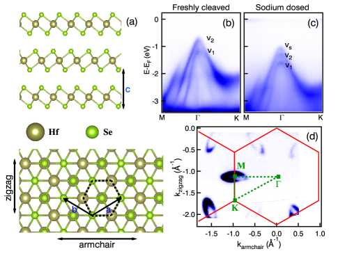
Our 1T-HfSe2 single crystals were grown using a flux growth method and cleaved in ultrahigh vacuum at pressures below 210-11 torr, providing a pristine surface. The 1T-HfSe2 layered structure resembles CdI2, by featuring Se-Hf in octahedral coordination. Each Se layer within HfSe2 is A-B stacked perpendicular to the c-axis, sandwiched by Hf layers with lattice constants a = 3.71-3.74 and c = 6.14 (see Fig. 1(a)) hflat1 ; hflat2 . Our ARPES measurements were performed at BL 10.0.1 of the Advanced Light Source (USA) and BL 10.2R BaDElPh of the Elettra Sincrotrone Trieste (ITA). The photon energies of s- and p- polarised light were set to be 20-80 eV with energy and angular resolution of 10-20 meV and 0.2o, respectively. The sample temperature was set to around 40-80 K. Surface sodium depositions were achieved using a SAES Getter evaporation source.
Fig. 1(b) and (c) show the ARPES measurement of the HfSe2 electronic structure for the pristine and sodium-evaporated samples. The electronic structure of our pristine HfSe2 along the M--K direction is comparable with the bulk, as obtained in previous experiments and calculations Hfcal1 ; hfarpes . There are no electronic states located at the Fermi level, as expected from the semiconducting bulk (Fig. 1(b)). Moreover, a nondegenerate valence band derived from one unit cell (two monolayers) labelled by v1 and v2 was observed, which can arise from weak interlayer interaction hfarpes ; vdwcorr1 . After sufficient sodium deposition (Fig. 1(c)), the valence band shifts to a higher binding energy while an additional band (vs) emerged at the point, which is a result of electron donation from the alkali metal to the host material CBdoping . The direct population leads to filling of conduction band gives rise to ellipsoidal Fermi contour, indicative of anisotropic behaviour at all M points of the Brillouin zone and consistent with previous calculations (Fig. 1(d)) Hfcal1 ; highmobi .
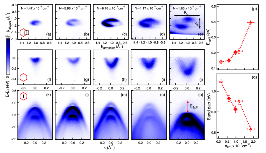
We investigated the evolution of the HfSe2 electronic structure as a function of electron doping, achieved by increasing exposure time for sodium evaporation (with constant current (I = 6.2 A)). As shown in Fig. 2(a)-2(e), by increasing exposure time, the surface carrier density, as determined by its Luttinger area (N2D = , where gv = 3 is valley multiplicity for all occupied ellipsoidal pockets, kS and kL are short and long ellipsoidal radii), increases with increasing time for the same sample. The maximum surface carrier density can reach or approximately 0.27 electrons per surface unit cell higher than those previously reported Riley_NEC ; CBdoping . This suggests that HfSe2 has a high capacity for extrinsic dopant atoms via its van der Waals (vdW) layer, making it suitable as a host material or substrate. We found a clear increase in the valence band splitting ( = vs-v2) at the valence band maximum, found by fitting the energy distribution curves (EDCs) around the point of two distinct valence bands up to 400 meV (Fig. 2(k)-2(o)), as summarised in Fig. 2(p)). By extracting the gap between the conduction band minimum (M point, Fig. 2 (f)-2(j)) and valence band maximum ( point, Fig. 2(k)-2(o)), we found a continuous decrease in the indirect band gap up to a maximum splitting of 280 meV (Fig. 2 (q)). This observation could be ascribed to surface accumulation or intercalation caused by the introduction of the alkali metal at the surface.
Unlike previous reports of alkali deposition on several TMDs Riley_NEC ; electricfield , our observed band splitting can not be explained by the introduction of a surface electric field from charge accumulation. For example, the existence of valence band splitting at K point can be obtained by applying an electric field at the WSe2 surface, but could not be seen at the point of HfSe2. This may be the critical difference between 1T and 2H symmetry (see the difference in Supplemental Material). In other words, the intercalation should be the dominant effect in HfSe2 system and a rationale is needed to include strain here.
Based on the experimental findings, we then calculated the band structure of HfSe2 under different strain conditions induced by sodium intercalation. Calculations were carried out within the framework of density functional theory with projector augmented wave potentials (PAW) cal1 as implemented in the VASP code. The PBE approximation is used for the exchange correlation terms cal2 ; cal3 with van der Waals corrections carried out using the DFT+D3 method vdwcorr1 . An 11 11 1 and 5 5 1 Monkhorst-Pack k-point grid were used for bulk and supercell calculations, respectively Monkhorst . The electron wave functions were described using a plane wave basis set with the energy cutoff at 520 eV.
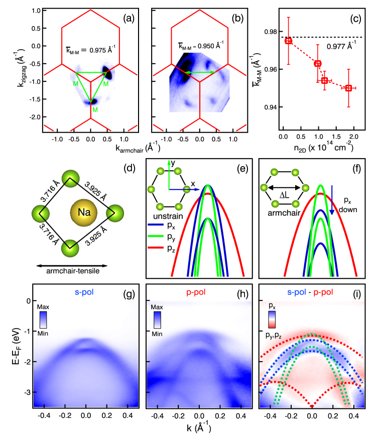
In addition, the Fermi surface maps spanning three M points of the Brillouin zone of lightly- and heavily-doped samples are shown in Fig. 3(a) and 3(b), respectively. By using distance of 0.977 (as given by ) for a fresh sample to be used as a reference, we found Brillouin zone shrinkage up to 2.76 , as determined by a decreasing of as a function of electron doping (Fig. 3(c)). This could be rationalised by the intercalation of sodium into HfSe2 layers, hence enlarging the unit cell in real space enlarge1 ; enlarge2 . Moreover, the Brillouin zone shrinkage appears larger in the reciprocal tensile direction than the zigzag direction, suggesting a preference for expansion in the armchair direction in real space. Fig. 3(d) represents the possibility of introducing armchair tensile strain when adding sodium at unit cell centre. The fully relaxed atomic structure of Na0.25HfSe2, illustrating the lattice distortion and expansion effects arising from the introduction of a single sodium atom into the centre of a 2 2 2 cell, are shown in the Supplemental Material.
The calculated electronic band structure of anisotropic lattice distortion in HfSe2 is supported by the experimental ARPES results, where three different hole-like bands are observed near the valence band maximum of HfSe2 arising from Se orbitals Hfcal1 . The most heavily ’hole-like’ band is , followed by then . Fig. 3(e) and 3(f) illustrate schematic band deformation arising from external uniaxial strain. In HfSe2, the top of the valence band is contributed to by Se p-orbitals, where px and py orbitals are degenerate at the valence band maximum, while the pz orbital is located at slightly higher binding energy (Fig. 3(e)). The relative positions of the orbitals can be rearranged by applying uniaxial strain. As shown in Fig. 3(f), the px orbital is shifted to higher binding energy resulting in the contribution of py to the valence band maximum under armchair tensile strain conditions. Light polarisation-dependent measurements are best suited to reconciling orbital ordering with those bands expected within our geometry Lewis_pol . Fig. 3(g) shows the electronic band structure measured by s-pol where the most intense bands are orbitals. In contrast, p-pol measurement reveals more orbitals than s-pol, where and appear most notable (Fig. 3(h)). Fig. 3(i) shows the intensity difference obtained by subtracting s- and p- pol data, clearly indicating the valence band splitting of and orbitals in our doped sample. Overall, it is shown that sodium evaporation/intercalation can lead to lattice distortion. The distorted HfSe2 prefers to rearrange in armchair tensile strain ZnO ; Ribb2 , as confirmed by our polarisation-dependent ARPES data (Fig. 3(i)).
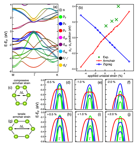
The ARPES results suggest that sodium atoms can occupy a maximum of 27 of surface unit cells, which is comparable to the computational Na0.25HfSe2 model. The increase in the valence band splitting brought on by sodium doping is a result of an increased uniaxial strain in the doped HfSe2 layer. Electronic structure calculations for HfSe2 have been performed under armchair and zigzag uniaxial strains ranging from -5 to 5. The unstrained orbital-projected electronic structure of HfSe2 is shown in Fig. 4(a) representing Se p-orbitals located at the top of valence band. Fig. 4(d)-4(j) represent the zoomed-in electronic structures around the point between -2 to +2 uniaxial armchair strain, where minus and plus signs indicate compressive (Fig. 4(c)) and tensile (Fig. 4(g)) strain respectively. The band deformation plays an important role in varying relative band positions (and therefore band gap) and valence band splittings in these calculations. The px(py) orbitals are shifted in energy monotonically while py(px) orbitals are essentially constant as a function of applied tensile(compressive) strain, resulting in opposite sign of valence band splitting. Regarding the two previously-mentioned in-plane p-orbital bands, which are degenerate at the valence band maximum for bulk HfSe2, applying uniaxial strain significantly lifts the degeneracy and therein changes the electronic band gap. The calculated valence band splitting (py - px) reaches 333 and -376 meV in 5% tensile and compressive armchair strain, respectively. The zigzag uniaxial strain has also been performed, yielding valence band splitting in the opposite direction (Fig. 4(b)). Larger valence band splittings obtained from the ARPES data (green marks in Fig. 4(b) were found as compared with the calculated tensile strain values. This may be describable by anisotropic lattice distortion in which the asymmetrically-enlarged lattice (tensile armchair strain) is compressed in the zigzag direction to maintain its volume. Overall however, we note that the observed orbital valence band splitting are generally consistent with armchair-tensile strain.
In summary, we have observed an increase in orbital valence band splitting, band gap shrinkage and anisotropic unit cell enlargement by evaporating sodium onto HfSe2 surfaces corresponding to 27% surface doping concentration (equivalent to 0.27 electrons donated per surface unit cell). Our experimental ARPES data are well-supported by computational DFT calculations of fully relaxed Na0.25HfSe2, where the calculations showed the HfSe2 layer anisotropically distorted with about 5 strain due to sodium intercalants. Overall, it can be concluded that the presence of effective armchair-tensile strain is induced by sodium intercalation. We have also demonstrated the possibility of orbital control at the valence band maximum with ’valley physics’. In future work, this could be achieved by applying opposite uniaxial strain by introduction of different cationic (Na, K) or anionic (Cl, Br) intercalants or ionic liquids. These observations support an overall understanding of doping/strain physics to facilitate exploration of novel phenomena among layered-TMDs. This could also be used as a direct technique for large-scale strain engineering in tuning optical and electronic properties as well as for straintronics such as nanoscale stress sensors and tuneable photonic devices straintronics ; apps .
Acknowledgements.
We acknowledge P. D. C. King, P. Songsiriritthigul and T. Kongnok for supplying helpful discussion. This work was supported by Thailand Research Fund (TRF) and Suranaree University of Technology (SUT) (Grant No. BRG5880010) and Research Fund for DPST Graduate with First Placement (Grant No. 021/2555). The computing resources were provided by Theoretical Computation Section, SLRI, Thailand. SS acknowledges the Royal Golden Jubilee Ph.D. Program (Grant no. PHD/0007/2555). We thank ALS and Elettra for the allocation of synchrotron radiation beamtimes. The Advanced Light Source is supported by the U.S. Department of Energy, Office of Science, User Facility under contract No. DE-AC02-05CH11231.References
- (1) J. A. Wilson and A. D. Yoffe, Adv. Phys. 18, 193 (1969).
- (2) B. Radisavljevic et al., Nat. Nanotechnol. 6, 147 (2011).
- (3) S. H. Lee et al., Nano Lett. 12, 3695 (2012).
- (4) J. M. Riley et al., Nat. Phys. 10, 835 (2014).
- (5) Q. H. Wang et al., Nat. Nanotechnol. 7, 699 (2012).
- (6) H. Zeng et al., Nat. Nanotechnol. 7, 490 (2012).
- (7) O. Lopez-Sanchez et al., Nat. Nanotechnol. 8, 497 (2013).
- (8) B. Radisavljevic, M. B. Whitwick, and A. Kis, ACS Nano 5, 9934 (2011).
- (9) T. Shen, A.V. Penumatcha, and J. Appenzeller, ACS Nano 10, 4712 (2016).
- (10) H. Guo et al., J. Phys. Chem. C 118, 7242 (2014).
- (11) J. F. Zhao et al., Phys. Rev. Lett. 99, 146401 (2007).
- (12) M. Chhowalla et al., Nat. Chem. 5, 263 (2013).
- (13) K. Radhakrishnan and M. Pilla, AIP Conf. Proc. 1004, 283 (2008).
- (14) S. Lebgue et al., Phys. Rev. X 3, 031002 (2013).
- (15) C. Gaiser et al., Phys. Rev. B 69, 075205 (2004).
- (16) R. Yue et al., ACS Nano 9, 474 (2015).
- (17) K. E. Aretouli et al., Appl. Phys. Lett. 106, 143105 (2015).
- (18) W. Zhang et al., Nano Res. 7, 1731 (2014).
- (19) M. Kang et al., Appl. Phys. Lett. 106, 143108 (2015).
- (20) L. F. Mattheiss Phys. Rev. B 8, 3719 (1973).
- (21) R. Coehoorn et al., Phys. Rev. B 35, 6195 (1987).
- (22) R. H. Friend and A. D. Yoffe, Adv. Phys. 36, 1 (1987).
- (23) K. Rossnagel New J. Phys. 12, 125018 (2010).
- (24) T. Eknapakul et al., Nano Lett. 14, 1312 (2014).
- (25) A. Varykhalov et al., Phys. Rev. Lett. 101, 157601 (2008).
- (26) C. Riedl et al., Phys. Rev. Lett. 103, 246804 (2009).
- (27) J. M. Riley et al., Nat. Nanotechnol. 10, 1043 (2015).
- (28) B. Ouyang et al., Appl. Phys. Lett. 107, 191903 (2015).
- (29) H. Fang et al., Nano Lett. 13, 1991 (2013).
- (30) A. Michail et al., Appl. Phys. Lett. 108, 173102 (2016).
- (31) A. Tarasov et al., Adv. Mater. 27, 1175 (2015).
- (32) H. J. Conley et al., Nano Lett. 13, 3626 (2013).
- (33) Y. Ma et al., ACS Nano 6, 1695 (2012).
- (34) Y. Zhou et al., ACS Nano 6, 9727 (2012).
- (35) A. E. Maniadaki, G. Kopidakis, and I. N. Remediakis, Solid State Commun. 227, 33 (2016).
- (36) L. Brey, N. E. Christensen, and M. Cardona, Phys. Rev. B 36, 2638 (1987).
- (37) C. Priester, G. Allan, and M. Lannoo, Phys. Rev. B 37, 8519 (1988).
- (38) Y. Zhang et al., Nat. Nanotechnol. 9, 111 (2014).
- (39) D. Le et al., J. Phys.: Condens. Matter 27, 182201 (2015).
- (40) M. Silver et al., Phys. Rev. B 46, 6781 (1992).
- (41) X.-G. Zheng, H. Kuriyaki, and K. Hirakawa, J. Phys. Soc. Jpn. 58, 622 (1989).
- (42) S. Grimme, S. Ehrlich, and L. Goerigk, J. Comp. Chem. 32, 1456 (2011).
- (43) H. Yuan et al., Nat. Phys. 9, 563 (2013).
- (44) P. E. Blchl Phys. Rev. B 50, 17953 (1994).
- (45) J. P. Perdew, K. Burke, and M. Ernzerhof, Phys. Rev. Lett. 77, 3865 (1996).
- (46) J. P. Perdew, K. Burke, and M. Ernzerhof, Phys. Rev. Lett. 78, 1396 (1997).
- (47) H. J. Monkhorst and J. D. Pack, Phys. Rev. B 13, 5188 (1976).
- (48) X. Wang et al., ACS Nano 8, 11394 (2014).
- (49) D. Yang et al., Phys. Rev. B 43, 12053 (1991).
- (50) B. Ouyang, Z. Mi, and J. Song, J. Phys. Chem. C 120, 8927 (2016).
- (51) A. Hansson and S. Stafstrm, Phys. Rev. B 72, 125420 (2005).
- (52) K. Leng et al., ACS Nano 10, 9208 (2016).
- (53) L. Bawden et al., Sci. Adv. 1, e1500495 (2015).
- (54) A. Fathalian and J. Jalilian, Phys. Lett. A 374, 46 (2010).
- (55) X. Peng and S. Velasquez, Appl. Phys. Lett. 98, 023112 (2011).
- (56) W. Wei, Y. Dai, and B. Huang, Phys. Chem. Chem. Phys. 19, 663 (2017).
- (57) Y. Jung, Y. Zhou, and J. J. Cha, Inorg. Chem. Front. 3, 452 (2016).