Kavli Institute for Nanoscale Science, Cornell University, Ithaca – NY, 14853, USA \alsoaffiliationKavli Institute for Nanoscale Science, Cornell University, Ithaca – NY, 14853, USA
Spin-orbit torques in NbSe2/Permalloy bilayers
Abstract
We present measurements of current-induced spin-orbit torques generated by NbSe2, a fully-metallic transition-metal dichalcogenide material, made using the spin-torque ferromagnetic resonance (ST-FMR) technique with NbSe2/Permalloy bilayers. In addition to the out-of-plane Oersted torque expected from current flow in the metallic NbSe2 layer, we also observe an in-plane antidamping torque with torque conductivity (m)-1 and indications of a weak field-like contribution to the out-of-plane torque oriented opposite to the Oersted torque. Furthermore, in some samples we also measure an in-plane field-like torque with the form , where is the Permalloy magnetization direction and is perpendicular to the sample plane. The size of this component varies strongly between samples and is not correlated with the NbSe2 thickness. A torque of this form is not allowed by the bulk symmetries of NbSe2, but is consistent with symmetry breaking by a uniaxial strain that might result during device fabrication.
Current-induced spin torques generated by materials with large spin-orbit coupling (SOC), such as heavy metals 1, 2, 3 and topological insulators 4, 5, are candidates to enable a new generation of efficient non-volatile magnetic memories. Several research groups have recently considered the possibility that some 2-dimensional (2D) materials might also be used as sources of spin-orbit torque (SOT) 6, 7, 8, 9, 10. For example, 2D transition metal dichalcogenides 11 (TMDs) can possess strong SOC and are easily incorporated into device heterostructures with clean, atomically-precise interfaces. Initial studies of the SOT originating from the TMD semiconductors MoS2 7, 6, 8 and WSe2 7, grown by chemical vapor deposition, reported nonzero spin-torque conductivities, but disagreed as to whether the dominant torque is field-like or antidamping-like. Our research group has measured SOTs in WTe2/permalloy samples in which semi-metallic WTe2 layers were prepared by exfoliation, and observed an out-of-plane antidamping SOT component made possible by the low crystal symmetry of WTe2, as well as a more-conventional in-plane anti-damping SOT and an out-of-plane field-like torque due to the Oersted field 9, 10.
For magnetic memory applications it is of particular interest to explore materials which combine high electrical conductivity, , and strong SOC, . Here we report the first measurements of SOTs generated by a fully-metallic TMD, NbSe2, with 6 105 (m)-1 in our devices and = 76 meV 12. For comparison, the previously-measured semiconducting TMDs MoS2 and WS2 have typical electrical conductivities 10-6 (m)-1 and SOC energies = 0 - 40 meV 13, 14 while for for semi-metallic WTe2 104 (m)-1 and = 15 meV 9, 10, 15.
Our spin-torque ferromagnetic resonance (ST-FMR) measurements on NbSe2/Permalloy (Py) bilayers reveal small but nonzero SOTs, corresponding to spin-torque conductivities of order or less than (m)-1, about a factor of 100 weaker than the spin-torque conductivities generated by Pt or Bi2Se3 at room temperature 16, 5. To probe the mechanisms of these SOTs we perform systematic studies as a function of the NbSe2 thickness, , and the angle of applied magnetic field. We measure an in-plane antidamping SOT component that is only weakly dependent of , remaining sizable down to a single NbSe2 layer – suggesting an interfacial origin. We also observe a field-like out-of-plane torque that scales linearly with for sufficiently thick ( 5 nm) samples, indicating that in this regime the torque is dominated by a current-generated Oersted field. However, for devices with smaller number of NbSe2 layers ( 5 nm), the out-of-plane torque is weaker than the value expected from the field alone, and, for a single NbSe2 layer we observe a reversal of the direction of the field-like out-of-plane torque. These deviations could be the result of either an interfacial out-of-plane field-like SOT directed opposite to the Oersted torque, or possibly to non-uniform charge current flow in the Py layer such that the current within the Py generates a nonzero net Oersted field acting on the Py.
Interestingly, by performing systematic measurements as a function of the angle of an in-plane magnetic field we detect in some samples the presence of an additional in-plane torque that is field-like with the form , where is the Py magnetization direction. This torque is not allowed by symmetry considerations for the bulk NbSe2 crystal structure 9. We propose that the presence of this torque component is due to a strain-induced symmetry breaking, e.g., a unidirectional strain in the NbSe2 layer generated during the processs of exfoliation and sample fabrication 17.
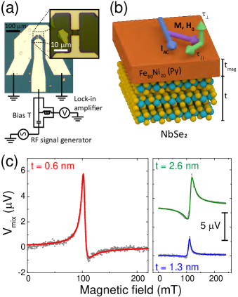
We prepare our samples by mechanically exfoliating a bulk synthetic NbSe2 crystal (HQgraphene) onto an intrinsic Si wafer with a 1-m-thick SiO2 layer thermally grown on the surface. The mechanical exfoliation is performed under vacuum (at pressures below 10-6 Torr) in the load-lock chamber of our sputter system, and the samples are loaded into the sputtering chamber without breaking vacuum. We then deposit 6 nm of Py by grazing angle ( 5∘) sputtering followed by 1.2 nm of Al, which oxidizes completely upon contact with atmosphere and serves as a capping layer. We have previously demonstrated that the grazing angle sputter deposition causes little to no damage to our TMD crystals 9. The NbSe2 flakes are identified by optical contrast, and their thicknesses and morphology are determined by atomic force microscopy (AFM). In order to avoid artifacts in our measurements due to roughness of the ferromagnetic layer, we selected only flat flakes with RMS surface roughness below 0.4 nm, measured by AFM in an area of 1x1 m2, and with no steps in the TMD crystals over the device area. We then pattern the NbSe2/Py bilayers into a bar shape with a well-defined length and width by using electron beam lithography followed by Ar+ ion milling. As a final step, we define Ti/Pt (5/75 nm) contacts in the shape of a coplanar waveguide using electron beam lithography followed by metal sputtering deposition. An optical micrograph of a finished device is shown in Figure 1a.
To measure the SOTs, we use the ST-FMR technique 1, 5, 9 in which an alternating microwave-frequency current () (with frequencies f = 7 - 12 GHz) is applied within the sample plane. Current-induced torques cause the magnetization of the ferromagnet to precess. By applying an external magnetic field at an angle with respect to , we set the direction of and the characteristic ferromagnetic resonance frequency of the ferromagnet (Figure 1b). The precession of the magnetization creates a time-dependent change of the device resistance due to the anisotropic magnetoresistance (AMR) of the ferromagnetic layer. This change in resistance mixes with generating a DC voltage across the NbSe2/Py bar (Vmix). The signal-to-noise ratio is maximized by modulating the amplitude of at low frequencies and detecting Vmix using a lock-in amplifier. The circuit geometry is shown in Figure 1a. All measurements are performed at room temperature unless indicated.
When the ferromagnetic resonance frequency matches , Vmix shows a resonance peak with a lineshape that can be described as: , where is a symmetric Lorentzian with amplitude proportional to the in-plane component of the torque (), and an antisymmetric Lorentzian with amplitude proportional to the out-of-plane component of the torque (). This allows the separation of the two torque components by fitting a measurement of Vmix as a function of . The two torques components are related to the amplitudes of the Lorentzians by 1, 5:
| (1) |
| (2) |
where is the device resistance, is the angle between and , is the effective magnetization of the Py layer, composed by the saturation magnetization and anisotropy terms, is the Gilbert damping of the Py, is the gyromagnetic ratio, is the vacuum permittivity, and is the resonance field. The term is due to the AMR in the Py layer. For our devices we have 0.8 T and 0.01 as obtained by the ST-FMR resonance frequency and linewidth, respectively, and is measured directly by measuring the device’s resistance as a function of . The current is calibrated by using a network analyzer to measure transmitted and reflected microwave powers ( and ).
Resonance curves for one, two, and four NbSe2 monolayers devices ( = 0.6, 1.3, and 2.6 nm, respectively) with = 9 GHz, applied RF power = 5 dBm and = 130∘ are shown in Fig. 1c, where the gray points represent experimental data and the fits are shown by the solid lines. Two important features are illustrated by these curves: the ratio between the amplitude of the symmetric and antisymmetric Lorentzians decreases with the increase of , and the sign of the antisymmetric component flips sign between the mono- and bi- layer devices. For both the one and two layer-thick devices, the lineshape is dominated by the symmetric component of the Lorentzian, meaning that the in-plane SOT is dominant over the out-of-plane component.
Our observation of both symmetric and antisymmetric components in the ST-FMR resonance is qualitatively similar to the results of Ref. 6 on MoS2/Py devices. The presence of both field-like and damping-like interfacial torques is consistent with general considerations of interfacial spin-orbit torques 18, 19, 20. However, a more recent measurement on MoS2/CoFeB and WSe2/CoFeB structures using a second harmonic Hall technique was unable to measure any in-plane SOT and attributed the large symmetric Lorentzian measured in Ref. 6 to spin-pumping combined with an inverse Rashba-Edelstein effect, rather than a spin-orbit torque 7. We can tell that the symmetric ST-FMR resonance signal we observe is not due primarily to a spin-pumping effect because this would require an unphysically-large spin-to-charge conversion factor (see Supplementary Information).
The symmetries and mechanisms of the SOTs can be analyzed in more detail by performing ST-FMR measurements as a function of the magnetic-field angle as and both depend upon . The contributions to the expected angular dependence can be understood as follows. Part of the angular dependence arises from the AMR in the bilayer, which contributes the dependence (see Eqs. 1 and 2). Many current-induced torques have a dependence (e.g. in-plane antidamping torques due to standard spin Hall or Rashba-Edelstein Effects, and the field-like out-of-plane torque due to the Oersted field), leading to an overall angular dependence . However, additional torque components can arise in systems with lower-symmetry 21, 22, such as WTe2 9, 10 and some semiconductor alloys 23, 24, 25, 26, 27.
The angular dependence we measure for the antisymmetric and symmetric components of the ST-FMR resonances of NbSe2/Py samples are shown in Fig. 2 for devices with monolayer (a,b) and bilayer (c,d) NbSe2. The angular dependence of the antisymmetric components for both samples is consistent with a simple form, illustrating that the out-of-plane torque has the usual dependence expected for a field-like out-of-plane torque. However, the symmetric ST-FMR components deviate from this form. We have performed more general fits (black lines in Fig. 2) for both components to the forms:
| (3) |
| (4) |
corresponding to the inclusion of additional angle-independent torques and such that the in-plane torque is and the out-of-plane torque is (where , , , and are independent of ). The vector forms of these additional torque components correspond to and . We find that this generalization greatly improves the fits for the symmetric ST-FMR components, with nonzero values for both and , and with the results for the monolayer sample indicating . For the bilayer sample the contribution from is less prominent but still clearly nonzero, while for both samples the fits to the antisymmetric component gives = 0 within the experimental resolution.
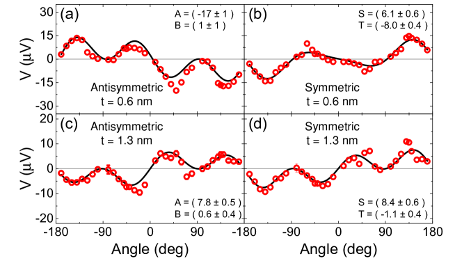
This result is curious in several ways. First, for the usual 2H-NbSe2 structure (space group P63/mmc) 28, the NbSe2/Py interface reduces to the space group P3m1 containing the identity, two 3-fold rotations, and three mirror planes. This set of symmetries forbids the presence of both of the torque terms and . However, any uniaxial strain will break the three-fold rotational symmetry and reduce the mirror symmetries to a single mirror plane or lower, depending on the alignment of the strain axis to the crystal axes. If there is a uniaxial strain, the torque terms or become symmetry-allowed, and in the case of a remaining mirror plane, the applied electrical current must have a component perpendicular to this plane. This situation is analogous to the strain-induced valley magnetoelectic effect observed in MoS2 monolayers 17.
We note, though, that both and are subject to the same symmetry constraints, so it is curious that remains zero even when broken symmetries allow . Furthermore, the result we find in the (presumably strained) NbSe2/Py samples (, ) is opposite to the results in WTe2/Py samples (, ) 9, 10 where a similar low-symmetry state is intrinsic to the WTe2 crystal structure. This suggests that the existence of the torque components and depend on more than the nature of the global broken symmetries, but also on microscopic factors like the nature of the atomic orbitals that contribute to charge and spin transport.
We investigated the extent to which the different torque components , , , and depend on the NbSe2 thickness, , by performing ST-FMR measurements as a function of applied magnetic field angle for a collection of different devices with different values of , while keeping the Py thickness fixed ( = 6 nm). These strengths of each torque component are linear in the current and voltage applied to the sample, and because the electric field across the device can be more accurately determined than the separate current densities through each of the individual layers in our devices (NbSe2 and Py), we express the torque strengths as torque conductivities, in units of ()()-1, where = , , , or corresponds to the different torque components, is the electric field, is the reduced Plank’s constant and the electron charge. We plot the thickness dependence of , , and in Fig. 3. The component is zero within experimental error for all of the samples measured.
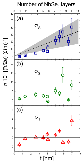
For the out-of-plane field-like torque conductivity we observe a clear increase with increasing NbSe2 thickness (Fig. 3a). For our thicker devices the magnitude of agrees with our estimation of the Oersted-field contribution () due to the current flowing in the NbSe2 layer. However, for the thinner ( 5 nm) devices, is significantly lower than our estimate for the Oersted contribution , and then the sign of is reversed for the monolayer device (see Fig. 1c). This behavior at small NbSe2 thicknesses suggests the presence of an interfacial field-like SOT that opposes the Oersted contribution. However, the size of the reversed SOT is sufficiently small that it is difficult to rule out possible alternative mechanisms such as a spatially non-uniform current density through the thickness of the Py layer. (Nonzero antisymmetric ST-FMR resonances can be observed even in single-layer Py samples, and have been ascribed to this mechanism 1, 29.)
The in-plane damping-like torque component (Fig. 3b) has at most a weak dependence on , and possesses a non-zero value all the way down to a single NbSe2 layer. The small apparent increase of with increasing could arise from a bulk contribution, such as the spin Hall effect. However, the nonzero value of this term down to a single NbSe2 layer suggests a sizable interfacial SOT. The value of for the thinnest samples ( 3 ) has a magnitude similar to reports for other TMDs, such as MoS2 6 and WTe2 9, but it is significantly below the values for Pt/ferromagnet bilayers 16 and topological insulators at room temperature 5 ( ).
For the in-plane field-like torque that is forbidden by symmetry for unstrained NbSe2 (Fig. 3c), we do not observe any systematic trend in the torque conductivity as a function of . While for a few of our devices, both the sign and magnitude of this torque term seem uncorrelated with the thickness of the NbSe2 layer. The lack of correlation between and is in agreement with our assumption that this term arises due to strain in our samples since we do not control this parameter. Strain-controlled experiments 17 could be performed in order to confirm this assumption and better constrain the microscopic origin of this extra torque term.
We also performed temperature dependence measurements for a sample showing all three torque components: , , and (see Supplementary Information), with . We observe only a weak temperature dependence for the torque ratio and a slightly stronger temperature dependence for . The weak temperature dependence of the interfacial SOTs in TMD/ferromagnet bilayers is in agreement with previous studies on semiconducting TMDs 7.
In summary, we report current induced SOTs in NbSe2/Py bilayers. The in-plane antidamping-like term has only a very weak dependence with , with values for the spin torque conductivity comparable to other TMDs. For thin NbSe2 layers, the out-of-plane SOT component for thin NbSe2 layers is significantly smaller than the estimate Oersted-field contribution, with a sign reversal for a monolayer of NbSe2. In additional to these expected torque components, we also observe the presence of a SOT with the form which is forbidden by the bulk symmetry of the NbSe2 crystal, but can arise in the presence of strain.
We thank R. A. Buhrman for valuable discussions and comments on the manuscript. This work was supported by the Kavli Institute at Cornell for Nanoscale Science, the Netherlands Organization for Scientific Research (NWO Rubicon 680-50-1311), the National Science Foundation (DMR-1406333, DMR-1708499), and the Army Research Office (W911NF-15-1-0447). G.M.S. acknowledges support by a National Science Foundation Graduate Research Fellowship under Grant No. DGE-1144153. This work made use of the NSF-supported Cornell Nanoscale Facility (ECCS-1542081) and the Cornell Center for Materials Research Shared Facilities, which are supported through the NSF MRSEC Program (DMR-1719875).
References
- Liu et al. 2011 Liu, L.; Moriyama, T.; Ralph, D. C.; Buhrman, R. A. Physical Review Letters 2011, 106, 036601
- Miron et al. 2011 Miron, I. M.; Garello, K.; Gaudin, G.; Zermatten, P.-J.; Costache, M. V.; Auffret, S.; Bandiera, S.; Rodmacq, B.; Schuhl, A.; Gambardella, P. Nature 2011, 476, 189–193
- Pai et al. 2012 Pai, C. F.; Liu, L.; Li, Y.; Tseng, H. W.; Ralph, D. C.; Buhrman, R. A. Applied Physics Letters 2012, 101, 122404
- Fan et al. 2014 Fan, Y. et al. Nature Materials 2014, 13, 699–704
- Mellnik et al. 2014 Mellnik, A. R.; Lee, J. S.; Richardella, A.; Grab, J. L.; Mintun, P. J.; Fischer, M. H.; Vaezi, A.; Manchon, A.; Kim, E.-A.; Samarth, N.; Ralph, D. C. Nature 2014, 511, 449
- Zhang et al. 2016 Zhang, W.; Sklenar, J.; Hsu, B.; Jiang, W.; Jungfleisch, M. B.; Xiao, J.; Fradin, F. Y.; Liu, Y.; Pearson, J. E.; Ketterson, J. B.; Yang, Z.; Hoffmann, A. APL Materials 2016, 4, 032302
- Shao et al. 2016 Shao, Q.; Yu, G.; Lan, Y. W.; Shi, Y.; Li, M. Y.; Zheng, C.; Zhu, X.; Li, L. J.; Amiri, P. K.; Wang, K. L. Nano Letters 2016, 16, 7514–7520
- Cheng et al. 2015 Cheng, C.; Collet, M.; Sánchez, J.-C. R.; Ivanovskaya, V.; Dlubak, B.; Seneor, P.; Fert, A.; Kim, H.; Han, G. H.; Lee, Y. H.; Yang, H.; Anane, A. arXiv:1510.03451 2015, 1510.03451
- MacNeill et al. 2017 MacNeill, D.; Stiehl, G. M.; Guimaraes, M. H. D.; Buhrman, R. A.; Park, J.; Ralph, D. C. Nature Physics 2017, 13, 300–305
- MacNeill et al. 2017 MacNeill, D.; Stiehl, G. M.; Guimarães, M. H. D.; Reynolds, N. D.; Buhrman, R. A.; Ralph, D. C. Physical Review B 2017, 96, 054450
- Manzeli et al. 2017 Manzeli, S.; Ovchinnikov, D.; Pasquier, D.; Yazyev, O. V.; Kis, A. Nature Reviews Materials 2017, 2, 17033
- Xi et al. 2016 Xi, X.; Wang, Z.; Zhao, W.; Park, J.-H.; Law, K. T.; Berger, H.; Forró, L.; Shan, J.; Mak, K. F. Nature Physics 2016, 12, 139
- Liu et al. 2013 Liu, G. B.; Shan, W. Y.; Yao, Y.; Yao, W.; Xiao, D. Physical Review B 2013, 88, 085433
- Xu et al. 2014 Xu, X.; Yao, W.; Xiao, D.; Heinz, T. F. Nature Physics 2014, 10, 343–350
- Jiang et al. 2015 Jiang, J. et al. Phys. Rev. Lett. 2015, 115, 166601
- Nguyen et al. 2016 Nguyen, M.-H.; Ralph, D. C.; Buhrman, R. A. Physical Review Letters 2016, 116, 126601
- Lee et al. 2017 Lee, J.; Wang, Z.; Xie, H.; Mak, K. F.; Shan, J. Nature Materials 2017, 16, 887–891
- Amin and Stiles 2016 Amin, V. P.; Stiles, M. D. Phys. Rev. B 2016, 94, 104419
- Amin and Stiles 2016 Amin, V. P.; Stiles, M. D. Phys. Rev. B 2016, 94, 104420
- Kim et al. 2017 Kim, K.-W.; Lee, K.-J.; Sinova, J.; Lee, H.-W.; Stiles, M. D. Phys. Rev. B 2017, 96, 104438
- Garello et al. 2013 Garello, K.; Miron, I. M.; Avci, C. O.; Freimuth, F.; Mokrousov, Y.; Blügel, S.; Auffret, S.; Boulle, O.; Gaudin, G.; Gambardella, P. Nature Nanotechnology 2013, 8, 587–593
- Yu et al. 2014 Yu, G. et al. Nature Nanotechnology 2014, 9, 548–554
- Chernyshov et al. 2009 Chernyshov, A.; Overby, M.; Liu, X.; Furdyna, J. K.; Lyanda-Geller, Y.; Rokhinson, L. P. Nature Physics 2009, 5, 656–659
- Endo et al. 2010 Endo, M.; Matsukura, F.; Ohno, H. Applied Physics Letters 2010, 97, 222501
- Fang et al. 2011 Fang, D.; Kurebayashi, H.; Wunderlich, J.; Výborný, K.; Zârbo, L. P.; Campion, R. P.; Casiraghi, A.; Gallagher, B. L.; Jungwirth, T.; Ferguson, A. J. Nature Nanotechnology 2011, 6, 413–417
- Skinner et al. 2015 Skinner, T. D.; Olejník, K.; Cunningham, L. K.; Kurebayashi, H.; Campion, R. P.; Gallagher, B. L.; Jungwirth, T.; Ferguson, A. J. Nature Communications 2015, 6, 6730
- Ciccarelli et al. 2016 Ciccarelli, C.; Anderson, L.; Tshitoyan, V.; Ferguson, A. J.; Gerhard, F.; Gould, C.; Molenkamp, L. W.; Gayles, J.; Železný, J.; Šmejkal, L.; Yuan, Z.; Sinova, J.; Freimuth, F.; Jungwirth, T. Nature Physics 2016, 12, 855–860
- Ribeiro-Soares et al. 2014 Ribeiro-Soares, J.; Almeida, R. M.; Barros, E. B.; Araujo, P. T.; Dresselhaus, M. S.; Cançado, L. G.; Jorio, A. Physical Review B 2014, 90, 115438
- Emori et al. 2016 Emori, S.; Nan, T.; Belkessam, A. M.; Wang, X.; Matyushov, A. D.; Babroski, C. J.; Gao, Y.; Lin, H.; Sun, N. X. Phys. Rev. B 2016, 93, 180402