Large Landau level splitting with tunable one-dimensional graphene superlattice probed by magneto capacitance measurements
Abstract
The unique zero energy Landau Level of graphene has a particle-hole symmetry in the bulk, which is lifted at the boundary leading to a splitting into two chiral edge modes. It has long been theoretically predicted that the splitting of the zero-energy Landau level inside the bulk can lead to many interesting physics, such as quantum spin Hall effect, Dirac like singular points of the chiral edge modes, and others. However, so far the obtained splitting with high-magnetic field even on a hBN substrate are not amenable to experimental detection, and functionality. Guided by theoretical calculations, here we produce a large gap zero-energy Landau level splitting ( 150 meV) with the usage of a one-dimensional (1D) superlattice potential. We have created tunable 1D superlattice in a hBN encapsulated graphene device using an array of metal gates with a period of 100 nm. The Landau level spectrum is visualized by measuring magneto capacitance spectroscopy. We monitor the splitting of the zeroth Landau level as a function of superlattice potential. The observed splitting energy is an order higher in magnitude compared to the previous studies of splitting due to the symmetry breaking in pristine graphene. The origin of such large Landau level spitting in 1D potential is explained with a degenerate perturbation theory. We find that owing to the periodic potential, the Landau level becomes dispersive, and acquires sharp peaks at the tunable band edges. Our study will pave the way to create the tunable 1D periodic structure for multi-functionalization and device application like graphene electronic circuits from appropriately engineered periodic patterns in near future.
I Introduction
One dimensional (1D) periodic superlattice potential has been a subject of considerable experimental and theoretical interest in condensed matter physics for decadesTsu and Esaki (1973); Tsu (2010). Graphene and its superlattice structures like Moire patternPletikosić et al. (2009); Yankowitz et al. (2012) have emerged a new play ground in recent years for both fundamentally due to its chiral nature as well as application point of view. Interesting electronic and transport phenomena such as, Klein tunnellingKatsnelson et al. (2006), electron collimationPark et al. (2008a), lensingCheianov et al. (2007), emergence of cloned Dirac pointsPonomarenko et al. (2013); Hunt et al. (2013), self similar recursive energy spectrum such as Hofstadter butterflyDean et al. (2013); Hunt et al. (2013), topological phases like floquet topological insulator Usaj et al. (2014) and different topological aspects, such as change in winding number as well as different scattering mechanisms (Wang et al., 2015) have been demonstrated based on graphene superlattice.
There have been several theoretical studies on 1D graphene superlattice and one of the main findings is that 1D periodic potential in graphene will give rise to new type of Dirac cones at zero energy as well as anisotropic Fermi velocity renormalization(Park et al., 2008b; Brey and Fertig, 2009; Wang and Zhu, 2010; Tan et al., 2011; Barbier et al., 2010; Killi et al., 2011). Some of them have been observed experimentally by looking at the appearance of the multiple resistance peaks as a function of superlattice potentialDubey et al. (2013); Drienovsky et al. (2014, 2017); Forsythe et al. (2017). However, contradictory conclusions have been drawn about the origin of multiple resistance peaks. No measurements have been performed to probe directly the renormalization of 1D superlattice band. Thus, direct probe of the superlattice band together with complete theoretical understanding of 1D periodic potential in graphene is crucial as it can shed light on the electronic properties as well as desirable for device applications.
The recent theoretical studies of 1D superlattice potential on the Landau level (LL) spectrum of graphene, in particular its effect on the zeroth LL has drawn considerable interest in the communityPark et al. (2009); Wu et al. (2012); Pal et al. (2012); Duque et al. (2017). The unique zeroth LL in pristine graphene having particle-hole symmetry gives rise to anomalous quantum Hall sequence compared to conventional semiconductor. It has been demonstrated both theoreticallyAbanin et al. (2006) as well as experimentallyZhang et al. (2006); Jiang et al. (2007); Checkelsky et al. (2008); Bolotin et al. (2009) that the degeneracy of the N = 0 LL of pristine graphene can be lifted by breaking the symmetries at high magnetic field, which gives rise to the splitting of the zeroth LLZhang et al. (2006); Jiang et al. (2007); Checkelsky et al. (2008); Bolotin et al. (2009) and manifests many interesting physics like quantum spin Hall state or helical state. Now, it has been shown theoretically that the application of 1D superlattice potential will change the degeneracy of the zeroth LL () as well as the Hall conductivity step sequence with the creation of new Dirac cones Park et al. (2009). It has been pointed out in ref Wu et al. (2012) that the effect of 1D superlattice on LL spectrum will depend on the competition between the magnetic length scale () versus period of the 1D potential (). In the weak limit ( > ) it will only change the degeneracy of the levels. However, in the intermediate ( ) and strong limit ( < ) the LL becomes dispersive and the ref Pal et al. (2012) predicted a large energy splitting of the Landau level (LL) comparable to the strength of the 1D supperlattice potential. However, there are no experimental observation of the renormalization of the LL spectrum in presence of 1D superlattice potential till date.
Quantum capacitanceLuryi (1988) measurements reveals significant insights to e-e interactionsEisenstein et al. (1992); Ilani et al. (2006); Yu et al. (2013); Chen et al. (2013); Zibrov et al. (2017), quantum correlationIlani et al. (2006), layer polarizationYoung et al. (2012); Hunt et al. (2017), many body physicsIlani et al. (2006); Zibrov et al. (2017); Hunt et al. (2017), Fermi velocity renormalizationYu et al. (2013); Chen et al. (2013)
and thermodynamic compressibilityPonomarenko et al. (2010); Dröscher et al. (2010); Young et al. (2012); Chen et al. (2013) in graphene. As the quantum capacitance is directly proportional to thermodynamic density of states (DOS), making it possible to directly probe the renormalization of 1D superlattice bandWu et al. (2015); Wang et al. (2013a). In this report, we have carried out resistance and quantum capacitance measurements on a boron nitride (hBN) encapsulated graphene device while 1D periodic superlattice potential and magnetic field applied. Our main observations are the following: (i) Inducing 1D periodic potential give rise to multiple resistance peaks at the Dirac point, which are reflected in the quantum capacitance data, consistent with the theoretical model. (ii) Magneto capacitance measurements have revealed two prominent features: at low superlattice potential 100 meV, broadening of LL as well as other LL was observed. At higher superlattice potential 100 meV, we observed evolution of the LL. First splitting into two sub levels, further increase in superlattice potential it starts interacting with the nearest Landau level. The observation of one order larger energy splitting ( meV) of the LL with the application of 1D superlattice potential is completely new emerging phenomena as compared to the observed splitting of zeroth LL at high magnetic field ( meV) due to symmetry breaking in pristine grapheneZhang et al. (2006). Our observations are compared with our corresponding theoretical calculations based on degenerate perturbation theory. We find that the Landau level becomes dispersive with the application of 1D superlattice potential and acquires sharp peaks at the tunable band edges exhibiting zeroth LL splitting.
II 1D superlattice and band structure
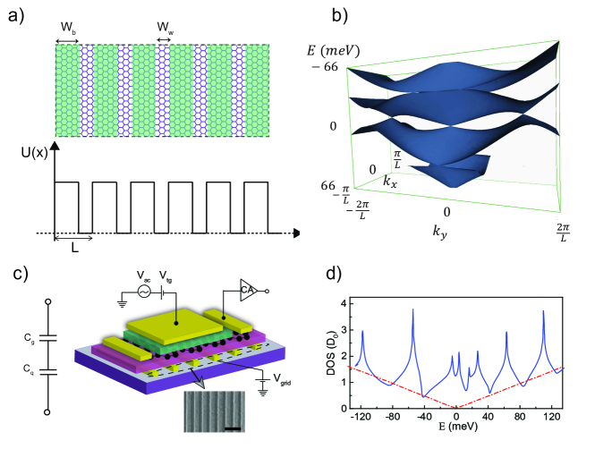
Fig. 1a shows the schematic of graphene placed on 1D artificial periodic superlattice. Here the periodic potential is applied along the direction with potential strength . Due to the chiral nature of charge carriers in graphene the group velocity does not change along the direction of applied potential, rather the group velocity gets renormalized along the direction perpendicular to the applied potential. It has also been shown that at the reduced zone boundary (MZ) there will be a band gap opening at the finite value of and its value will depend on the strength of the periodic potential Park et al. (2008b). The solution for square barrier superlattice is given as Barbier et al. (2010)
| (1) |
where , , , , ; are the width of the barrier and the well, respectively, is the energy and is the strength of the grid potential. The band structure calculated using this equation is shown in Fig. 1b with and for 130meV and the generated DOS is shown in Fig. 1d (Barbier et al. (2010)), where the dashed red line shows the DOS for zero superlattice potential. It can be seen from the Fig. 1d that dip in the DOS arises at the zone boundary; G (reciprocal lattice vector) = 2/L 40 meV, where L is the super lattice length ( 100 nm).
III Methods and measurement techniques
The schematic of the device architecture is shown in Fig. 1c. To realize 1D superlattice structures in graphene, we fabricated the device in the following way. At first Si/SiO2 substrate with 150 nm oxide was used to design the periodically spaced gold gates with barrier width nm and well nm using electron beam lithography followed by thermal deposition of Ti/Au (5/20) nm. The periodicity in this case was 100 nm. The inset in Fig. 1c shows the Scanning electron microscope image (SEM) of the gold grids. The details have been given in the supplementary information (S.I). Once the grids were ready, the top hexagonal boron nitride(hBN) and graphene were mechanically exfoliated separately onto piranha cleaned Si/SiO2 substrate and picked up individually one after another following the similar method as mentioned in RefWang et al. (2013b); Zomer et al. (2014). The bottom hBN was also picked up using the same procedure and the final hBN-graphene-hBN stack was transferred onto the gold grids as shown schematically in Fig. 1c (S1 for details). Top gate and source(drain) electrodes were patterned using electron beam lithography followed by thermal deposition of Cr(5nm)/Au(70nm). All the measurements are carried out Oxford cryostat at T = 2K. The capacitance was measured between the top gate and graphene.A small ac voltage of mV at a frequency of 5 kHz was applied to the top gate and the out of phase current was measured by lock in amplifier using home build current amplifier with a gain of 107Kretinin and Chung (2012) as described in our previous work Kuiri et al. (2015). The area of the top gate was 18 (determined by optical microscopy as well as by scanning electron microscopy) and the thickness of the top BN was 10-11 nm (determined by atomic force microscopy) yielding an effective top gate capacitance, Cg of 55 (for 10.5 nm) (S2-S4 for details).
IV Resistance Data
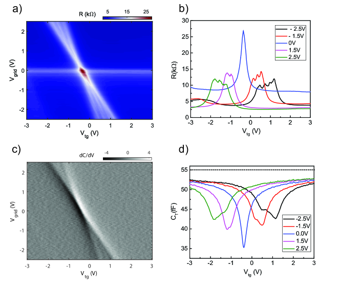
Two probe resistance measurement were performed using low frequency lock in technique by passing a small voltage between source-drain ( 100 ) and measuring the current through the channel. Fig. 2a shows the two terminal resistance color plot of the device as a function of grid voltage (Vgrid) and top gate voltage (Vtg), where the carrier density in graphene was tuned globally using periodic gold gate Vgrid and locally using Vtg. It can be seen that the Dirac point is located at (Vgrid,Vtg) = (0.0V, - 0.5V). For Vgrid = 0V, we can see the usual resistance gate voltage characteristic with Vtg as shown as a cut line in Fig. 2b. With the increase in superlattice potential i.e. at finite Vgrid, we see the appearance of additional peaks; for Vgrid = 1V we see two peaks, for Vgrid = 2.5V we see three peaks in the resistance data. The corresponding cut lines of Fig. 2a are shown in Fig. 2b for Vgrid = 1.5V and 2.5V and it can be seen that the additional resistance peaks appeared symmetrically for both positive and negative superlattice potentials.
The application of the Vgrid makes an unequal Fermi energy (EF) shifts in graphene; the EF shift will be more on top of the gold pillar ( nm) compared to the gap part ( nm). Thus, there will be a barrier between the two parts. The potential barrier, , defined by both gates and is given by (assuming equal barrier and well width )Dubey et al. (2013)
| (2) |
The only unknown parameter of the above equation is , which was estimated from the diagonal line of the charge neutrality point in Fig. 2a as described in SI (S5 for details).
The calculated barrier heights for Vgrid = 1.0V, 1.5V, 2.0V and 2.5V are 100 meV, 122 meV, 140 meV and 165 meV, respectively. We would like to comment that the above mentioned values are slightly overestimated as we have not considered the asymmetric grid potential as well as fringing effect of the electric fieldDubey et al. (2013).
It is evident that due to the super-lattice potential the multiple resistance peaks appear in Fig. 2a and 2b, which could be due to the dip in the DOS as shown theoretically in Fig. 1d and observed experimentally in Ref Dubey et al. (2013). However, the Ref Drienovsky et al. (2014) claims that the origin of multiple resistance peaks is due to Fabry Perot resonance. In order to see whether the multiple resistance peaks are indeed an effect of DOS modification or not we will now present our quantum capacitance data.
V Capacitance Data for B=0
In a parallel plate capacitor made of graphene and a normal metal, adding an electron to the graphene layer will cost not only the electrostatic potential energy but also kinetic energy. As a result, the measured capacitance will have both the geometrical term (potential) as well as the quantum term (kinetic) Luryi (1988). The total measured capacitance in such a system is given by
| (3) |
where, is the geometrical capacitance between the top gate and graphene, is the area of the graphene capacitor, and is the thermodynamic compressibility Yu et al. (2013). Cp is the parasitic capacitance associated with wiring plus stray capacitance. The quantum capacitance is defined as , which is directly proportional to DOS. The differential capacitance was measured using the similar techniques in Ref Kuiri et al. (2015). The parasitic capacitance (Cp 4.8 ) arising due to the electrical wiring and stray capacitance has been subtracted from the measured capacitance data. The details about the determination of parasitic capacitance () is shown in S3. Fig. 2c shows the 2D color plot of derivative of the total capacitance () measured as a function of and , where one can see the multiple broadened dips with increasing superlattice potential. Although the derivative of the capacitance shows three weaker dips at higher superlattice potential but the data is not as prominent as the multiple resistance peaks seen in Fig. 2a. Fig. 2d shows the cut lines of total capacitance () as a function of for several grid potentials.
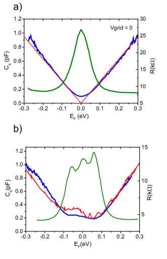
In order to understand the experimental capacitance data, we need to plot the quantum capacitance (Cq) as a function of the Fermi energy (). The can be calculated as and can be calculated from the charge conservation relation Xu et al. (2011); Dröscher et al. (2010); Yu et al. (2013) , where is the electronic charge. Fig. 3a shows the vs plot for zero grid voltage. The linear nature of the curve is reflecting the linear DOS of graphene. Using the DOS of graphene, = and is the Fermi velocity, we generate the theoretical curve in Fig. 3a (red dotted line). It can be noticed that the experimental does not vanish at signifying the residual charge in-homogeneity in the device and we estimate the Fermi energy broadening (). vs plot for ( meV) is shown in Fig. 3b. It can be seen how the DOS is modified near the Dirac point. The red line is the theoretically calculated DOS, with , where sharp features of theoretical DOS in Fig. 1d are broadened and one can notice that for (V) the DOS captures the expected linear nature. It can be seen the qualitative agreement between the experimental and theoretical data in Fig. 3b. Although the positions of the extreme two resistance peaks match exactly to the positions of the extreme two dips in Cq data but the signature of the middle peak in the resistance data is not evident in Cq. This discrepancy could be understood as follows: the resistance measurement is a directional dependent phenomena compared to the total DOS (Cq) measurement.
As shown in Ref Park et al. (2008b) that the application of super-lattice potential along the direction cannot open a gap along that direction () due to the Klien tunneling. Also there will be no gap in the perpendicular direction (). However, there will be gap opening at the reduced zone boundary in the certain directions of plane. It can be seen from our SEM image of the device (S4), the graphene is placed at an angle of 60 ∘ with the super-lattice direction. Thus, we believe that our measured longitudinal resistance predominantly capture the DOS along a certain direction of plane where as the quantum capacitance measurement captures the total DOS. We should note that the average separation of the resistance peaks in Fig. 3b is 50 meV. This energy separation is close to the expected DOS modifications at the reduced zone boundary position; EZ = G = 2/L 40meV for super-lattice length, L = 100nm.
VI Magneto-capacitance data
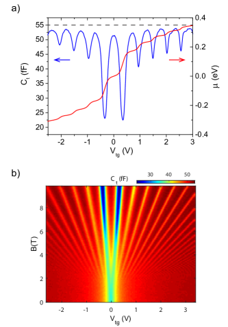
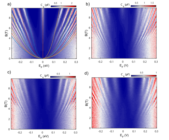
In order to see the effect of super-lattice potential on Landau Level (LL) spectrum we have carried out the quantum capacitance measurement in perpendicular magnetic field. In the presence of perpendicular magnetic field, the energy levels in monolayer graphene is quantized, with energy eigenvalues , where = 0, 1, 2,…is the Landau level index. Fig. 4a shows the total capacitance () as a function of at B = 9.8T for = 0V. The dips in the corresponds to the Landau-level gap. The Fig. 4b presents the total capacitance in a 2D color plot for several B showing the evolution of several Landau-levels. Although we have measured the by measuring the thickness of top hBN () by AFM and area () by SEM, but one can cross check that value from the Landau-level spectrum (Fig. 4b). First of all, the spacing (in gate voltage) between adjacent capacitance minimum around N = 0 LL remains similar to the spacing around the 1 LL confirming the sample is monolayer graphene as the LL degeneracy remains same for = 0, 1, 2, 3. The no of electron to fill the N = 0 LL is , where 4 comes from the 2 valley and 2 spin degrees of freedom. In the first order approximation we can write , where the is the average spacing between the adjacent minimum. The above relation gives 52, which is similar to the value obtained from measuring the thickness of top hBN (55 ) by AFM. As mentioned before using the charge conservation equation (), we have converted into or , which is shown in Fig. 4a, where one can clearly see the non-monotonic increment of with due to the presence of compressible and in-compressible regions in LL spectrum. Using the conversion method we have plotted the LL energy spectrum of graphene at zero super-lattice potential in Fig. 5a, where one can see the = 0, 1, 2….8 very clearly. The solid lines are the theoretical one based on . Agreement between the experimental data with the theory is quite noticeable upto 6T. Fig. 5b, 5c and 5d presents the LL spectrum for superlattice potentials, and , respectively. At the zeroth LL gets broadened. However, the most noticeable changed was observed beyond , where the N = 0 LL gets splitted and at higher super-lattice potential () the splitted N = 0 LL starts interacting with higher LLs as shown in S8.
The zeroth LL in monolayer graphene gives rise to anomalous quantum Hall sequenceAbanin et al. (2006) in graphene compared to conventional semiconductor. However, it is known from the literatureZhang et al. (2006); Jiang et al. (2007); Checkelsky et al. (2008); Bolotin et al. (2009) that the N = 0 LL degeneracy can be lifted by breaking the symmetries at high magnetic field, which gives rise to an insulating stateCheckelsky et al. (2009); Jiang et al. (2007); Bolotin et al. (2009) at the Dirac point. The common consensus is that the valley degeneracy gets lifted at higher B due to the coulomb interaction (, where is the magnetic length scale), which is a many body interaction physics. However, in order to see the insulating phase at LL ( meV at 10T) one needs to have extremely cleaner device (). As can be seen from Fig. 5a that we do not observe the splitting of the zeroth LL even upto 10T at U = 0 because of large meV in our device, but it gets splitted with the application of superlattice potential and splitting is very large meV. Thus, the large splitting of LL due to the 1D super-lattice potential in Fig. 5c and 5d is completely new, which has not been experimentally reported prior to this work. In the next paragraph we will discuss our theoretical calculation based on degenerate perturbation theory to calculate the DOS of the LL in the presence of 1D super-lattice potential. It turns out that indeed the zeorth LL gets broadened with a energy dispersion having a width comparable to the strength of superlatice potential and the DOS acquires an enhanced peak at the band edge resulting in a splitting around the zeroth LL.
VII Theory
What is so special about a 1D superlattice potential which enables large splitting of the zeroth LL, while the typical 2D superlattice potentials often fail to do so? We first give a heuristic argument, and supplement it with a theoretical calculation. The LLs are the quantized energy ( is the LL index) of the cyclotron orbits in real space. The cyclotron orbits are localized with Gaussian wavefunction, with its width determined by the magnetic length 111In the Landau gauge, the cyclotron orbitals are extended in one direction, and localized in the orthogonal direction. Here, without loosing generality, we assume the 1D potential is along the direction of the LL localization, while a similar physics can be reproduced with the other assumption. They are thus analogous to the ‘maximally localized Wannier orbitals’ with a localization length of . A weak periodic potential helps mobilizing these localized cyclotron orbits, with a range of wavevectors featuring the underlying periodicity of the superlattice potential. As a result the LLs acquire band dispersion . A 1D dispersion manifests sharp peaks in the density of states (DOS) at the top and bottom of the bands, and a dip in the low-energy spectral function. On the contrary, a 2D dispersion acquires a peak in the DOS in the low-energy region due to the van-Hove singularity. In what follows, the key message is that a 1D dispersion of the LL gives the impression of a well resolved splitting of the LL in the DOS, while a 2D potential produces an opposite effect.
We are in the sufficiently large magnetic field limit such that the LL spacing , where is the superlattice potential strength. In our samples, is tunable and thus at smaller values of the inter-LL hybridization or interaction can be neglected. Owing to the large degeneracy associated with the LLs, we can therefore incorporate the effects of the weak-periodic potential within a degenerate perturbation theory for a given LL. We solve the LL problem with the Landau gauge by assuming the vector potential , which produces a wavefunction that is extended in the -direction, but Gaussian like along the direction. So, we get , where is the Hermite polynomials, is the normalization constant. , where is the length of the periodic potential along the -direction, and is the magnetic length. The center of the cyclotron orbit lies at , where is the LL wavevector along the -direction. For such a state the first order perturbation correction to the LL is given by
| (4) |
where is the periodic potential. Without loosing generality, we assume that the 1D potential spans along the -direction, and thus it can be expanded in the Fourier basis as , where is determined by the nature of the periodic potential. We have a 1D square-like potential with a width , where is the width of intermediate region. However, the potential edge is a smooth function in and and one can assume a sinusoidal form, governing discrete values of .
We can now compute the matrix element of the perturbed Hamiltonian as
| (5) |
This equation is analogous to the tight-binding equation, and in this spirit, we refer the tight-binding hopping amplitude between the localized cyclotron orbits located at , and . In Eq. (5), the -integral gives the momentum conservation condition . The -integral gives different results for different LLs, and for the zeroth LL of present interest, we obtain
| (6) |
The absolute value of depends on . It depends linearly on the potential strength, as also obtained experimentally (see Fig. 6(c)). however increases exponentially on magnetic field, i.e, , where .
In the second quantization language, the effective Hamiltonian becomes
| (7) |
where denote the degenerate LLs with cyclotron orbits located at and . By doing the Fourier transformation , we obtain a dispersion of the LL along the -direction as
| (8) |
where is the periodicity of the superlattice potential. The total tight-binding energy dispersion of the LL is thus
| (9) |
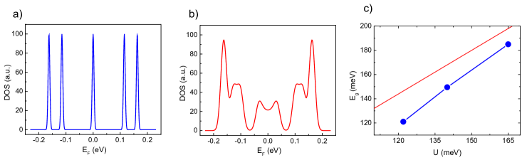
The bandwidth of the above dispersion is . The DOS at a given energy is defined as , where the group velocity . vanishes at , i.e. at the bottom and top of the bands. Therefore, the original LL acquires sharp peaks at the top and bottom of the dispersion in a 1D periodic lattice. The energy gap between the DOS peaks is . As mentioned in Eq. (6), , and hence increases linearly with , but exponentially with the magnetic field , both of which are consistent with experiments, as discussed in Fig. 6. The splitting decreases as we move to higher LL.
In Fig. 6, we show the DOS as a function of energy for graphene at a given magnetic field T, for the periodic potential , (Fig. 6a) and (Fig. 6b). Also including a (experimental) broadening of 30 meV, we notice that LL broadens for small superlattice potential, and then it splits into two for large superlattice potential for . For superlattice potential comparable to the LL gap , scattering between different LL becomes large, and higher LLs start mixing with each other, which has been experimentally observed as shown in S8. In Fig. 6c we compare the theoretical splitting (red line) of LL with the experimental one as a function of superlattice potential, where one can clearly see the qualitative agreement between the experimental results with the theoretical one. We believe the mismatch is due to the overestimated values of the barrier potential.
VIII Conclusion
In summary, we have demonstrated for the first time, quantum capacitance measurements in 1D graphene superlattice. We have observed band structure modification as a function of 1D superlattice potential strength at zero magnetic field is consistent with the theoretical prediction. At higher superlattice potential we have observed a large splitting ( 150 meV) of the zero Landau level. The renormalization of the LL spectrum due to 1D superlattice potential is compared with our theoretical calculation.
IX Acknowledgements
A.D thanks DST nanomission (DSTO-1470 and DSTO-1597) for the financial support.
References
- Tsu and Esaki (1973) R. Tsu and L. Esaki, Appl. Phys. Lett. 22, 562 (1973).
- Tsu (2010) R. Tsu, Superlattice to nanoelectronics (Elsevier, 2010).
- Pletikosić et al. (2009) I. Pletikosić, M. Kralj, P. Pervan, R. Brako, J. Coraux, A. T. N’Diaye, C. Busse, and T. Michely, Phys. Rev. Lett. 102, 056808 (2009).
- Yankowitz et al. (2012) M. Yankowitz, J. Xue, D. Cormode, J. D. Sanchez-Yamagishi, K. Watanabe, T. Taniguchi, P. Jarillo-Herrero, P. Jacquod, and B. J. LeRoy, Nature Physics 8, 382 (2012).
- Katsnelson et al. (2006) M. Katsnelson, K. Novoselov, and A. Geim, Nature Physics 2, 620 (2006).
- Park et al. (2008a) C.-H. Park, Y.-W. Son, L. Yang, M. L. Cohen, and S. G. Louie, Nano letters 8, 2920 (2008a).
- Cheianov et al. (2007) V. V. Cheianov, V. Fal’ko, and B. Altshuler, Science 315, 1252 (2007).
- Ponomarenko et al. (2013) L. Ponomarenko, R. Gorbachev, G. Yu, D. Elias, R. Jalil, A. Patel, A. Mishchenko, A. Mayorov, C. Woods, J. Wallbank, et al., Nature 497, 594 (2013).
- Hunt et al. (2013) B. Hunt, J. Sanchez-Yamagishi, A. Young, M. Yankowitz, B. J. LeRoy, K. Watanabe, T. Taniguchi, P. Moon, M. Koshino, P. Jarillo-Herrero, et al., Science 340, 1427 (2013).
- Dean et al. (2013) C. Dean, L. Wang, P. Maher, C. Forsythe, F. Ghahari, Y. Gao, J. Katoch, M. Ishigami, P. Moon, M. Koshino, et al., Nature 497, 598 (2013).
- Usaj et al. (2014) G. Usaj, P. M. Perez-Piskunow, L. E. F. Foa Torres, and C. A. Balseiro, Phys. Rev. B 90, 115423 (2014).
- Wang et al. (2015) P. Wang, B. Cheng, O. Martynov, T. Miao, L. Jing, T. Taniguchi, K. Watanabe, V. Aji, C. N. Lau, and M. Bockrath, Nano Lett. 15, 6395 (2015).
- Park et al. (2008b) C.-H. Park, L. Yang, Y.-W. Son, M. L. Cohen, and S. G. Louie, Nature Physics 4, 213 (2008b).
- Brey and Fertig (2009) L. Brey and H. A. Fertig, Phys. Rev. Lett. 103, 046809 (2009).
- Wang and Zhu (2010) L.-G. Wang and S.-Y. Zhu, Phys. Rev. B 81, 205444 (2010).
- Tan et al. (2011) L. Z. Tan, C.-H. Park, and S. G. Louie, Nano Lett. 11, 2596 (2011).
- Barbier et al. (2010) M. Barbier, P. Vasilopoulos, and F. M. Peeters, Phys. Rev. B 81, 075438 (2010).
- Killi et al. (2011) M. Killi, S. Wu, and A. Paramekanti, Phys. Rev. Lett. 107, 086801 (2011).
- Dubey et al. (2013) S. Dubey, V. Singh, A. K. Bhat, P. Parikh, S. Grover, R. Sensarma, V. Tripathi, K. Sengupta, and M. M. Deshmukh, Nano Lett. 13, 3990 (2013).
- Drienovsky et al. (2014) M. Drienovsky, F.-X. Schrettenbrunner, A. Sandner, D. Weiss, J. Eroms, M.-H. Liu, F. Tkatschenko, and K. Richter, Phys. Rev. B 89, 115421 (2014).
- Drienovsky et al. (2017) M. Drienovsky, A. Sandner, C. Baumgartner, M.-H. Liu, T. Taniguchi, K. Watanabe, K. Richter, D. Weiss, and J. Eroms, arXiv preprint arXiv:1703.05631 (2017).
- Forsythe et al. (2017) C. Forsythe, X. Zhou, T. Taniguchi, K. Watanabe, A. Pasupathy, P. Moon, M. Koshino, P. Kim, and C. R. Dean, arXiv preprint arXiv:1710.01365 (2017).
- Park et al. (2009) C.-H. Park, Y.-W. Son, L. Yang, M. L. Cohen, and S. G. Louie, Phys. Rev. Lett. 103, 046808 (2009).
- Wu et al. (2012) S. Wu, M. Killi, and A. Paramekanti, Phys. Rev. B 85, 195404 (2012).
- Pal et al. (2012) G. Pal, W. Apel, and L. Schweitzer, Phys. Rev. B 85, 235457 (2012).
- Duque et al. (2017) C. A. Duque, M. A. Hernández-Bertrán, A. L. Morales, and M. de Dios-Leyva, Journal of Applied Physics 121, 074301 (2017).
- Abanin et al. (2006) D. A. Abanin, P. A. Lee, and L. S. Levitov, Phys. Rev. Lett. 96, 176803 (2006).
- Zhang et al. (2006) Y. Zhang, Z. Jiang, J. P. Small, M. S. Purewal, Y.-W. Tan, M. Fazlollahi, J. D. Chudow, J. A. Jaszczak, H. L. Stormer, and P. Kim, Phys. Rev. Lett. 96, 136806 (2006).
- Jiang et al. (2007) Z. Jiang, Y. Zhang, H. L. Stormer, and P. Kim, Phys. Rev. Lett. 99, 106802 (2007).
- Checkelsky et al. (2008) J. G. Checkelsky, L. Li, and N. P. Ong, Phys. Rev. Lett. 100, 206801 (2008).
- Bolotin et al. (2009) K. I. Bolotin, F. Ghahari, M. D. Shulman, H. L. Stormer, and P. Kim, Nature 462, 196 (2009).
- Luryi (1988) S. Luryi, Appl. Phys. Lett. 52, 501 (1988).
- Eisenstein et al. (1992) J. P. Eisenstein, L. N. Pfeiffer, and K. W. West, Phys. Rev. Lett. 68, 674 (1992).
- Ilani et al. (2006) S. Ilani, L. A. Donev, M. Kindermann, and P. L. McEuen, Nature Physics 2, 687 (2006).
- Yu et al. (2013) G. Yu, R. Jalil, B. Belle, A. S. Mayorov, P. Blake, F. Schedin, S. V. Morozov, L. A. Ponomarenko, F. Chiappini, S. Wiedmann, et al., Proc. Natl. Acad. Sci. USA 110, 3282 (2013).
- Chen et al. (2013) X. Chen, L. Wang, W. Li, Y. Wang, Z. Wu, M. Zhang, Y. Han, Y. He, and N. Wang, Nano research 6, 619 (2013).
- Zibrov et al. (2017) A. Zibrov, C. Kometter, H. Zhou, E. Spanton, T. Taniguchi, K. Watanabe, M. Zaletel, and A. Young, Nature 549, 360 (2017).
- Young et al. (2012) A. F. Young, C. R. Dean, I. Meric, S. Sorgenfrei, H. Ren, K. Watanabe, T. Taniguchi, J. Hone, K. L. Shepard, and P. Kim, Phys. Rev. B 85, 235458 (2012).
- Hunt et al. (2017) B. Hunt, J. Li, A. Zibrov, L. Wang, T. Taniguchi, K. Watanabe, J. Hone, C. Dean, M. Zaletel, R. Ashoori, et al., Nature Communications 8, 948 (2017).
- Ponomarenko et al. (2010) L. A. Ponomarenko, R. Yang, R. V. Gorbachev, P. Blake, A. S. Mayorov, K. S. Novoselov, M. I. Katsnelson, and A. K. Geim, Phys. Rev. Lett. 105, 136801 (2010).
- Dröscher et al. (2010) S. Dröscher, P. Roulleau, F. Molitor, P. Studerus, C. Stampfer, K. Ensslin, and T. Ihn, Appl. Phys. Lett. 96, 152104 (2010).
- Wu et al. (2015) Z. Wu, Y. Han, J. Lin, W. Zhu, M. He, S. Xu, X. Chen, H. Lu, W. Ye, T. Han, Y. Wu, G. Long, J. Shen, R. Huang, L. Wang, Y. He, Y. Cai, R. Lortz, D. Su, and N. Wang, Phys. Rev. B 92, 075408 (2015).
- Wang et al. (2013a) L. Wang, Y. Wang, X. Chen, W. Zhu, C. Zhu, Z. Wu, Y. Han, M. Zhang, W. Li, Y. He, et al., Scientific reports 3 (2013a), 10.1038/srep02041.
- Wang et al. (2013b) L. Wang, I. Meric, P. Huang, Q. Gao, Y. Gao, H. Tran, T. Taniguchi, K. Watanabe, L. Campos, D. Muller, et al., Science 342, 614 (2013b).
- Zomer et al. (2014) P. J. Zomer, M. H. D. Guimarães, J. C. Brant, N. Tombros, and B. J. van Wees, Appl. Phys. Lett. 105, 013101 (2014).
- Kretinin and Chung (2012) A. V. Kretinin and Y. Chung, Rev. Sci. Instrum. 83, 084704 (2012).
- Kuiri et al. (2015) M. Kuiri, C. Kumar, B. Chakraborty, S. N. Gupta, M. H. Naik, M. Jain, A. Sood, and A. Das, Nanotechnology 26, 485704 (2015).
- Xu et al. (2011) H. Xu, Z. Zhang, Z. Wang, S. Wang, X. Liang, and L.-M. Peng, ACS Nano 5, 2340 (2011).
- Checkelsky et al. (2009) J. G. Checkelsky, L. Li, and N. Ong, Phys. Rev. B 79, 115434 (2009).
- Note (1) In the Landau gauge, the cyclotron orbitals are extended in one direction, and localized in the orthogonal direction. Here, without loosing generality, we assume the 1D potential is along the direction of the LL localization, while a similar physics can be reproduced with the other assumption.
See pages - of figss.pdf