and
Highly selective dry etching of GaP in the presence of AlGaP with a SiCl4/SF6 plasma
Abstract
We present an inductively coupled-plasma reactive-ion etching process that simultaneously provides both a high etch rate and unprecedented selectivity for gallium phosphide (GaP) in the presence of aluminum gallium phosphide (AlGaP). Utilizing mixtures of silicon tetrachloride (SiCl4) and sulfur hexafluoride (SF6), selectivities exceeding 2700:1 are achieved at GaP etch rates above 3000 nm/min. A design of experiments has been employed to investigate the influence of the inductively coupled-plasma power, the chamber pressure, the DC bias and the ratio of SiCl4 to SF6. The process enables the use of thin AlGaP stop layers even at aluminum contents of a few percent.
Keywords: gallium phosphide, aluminum gallium phosphide, selective etching, inductively-coupled-plasma reactive ion etching.
1 Introduction
III-V materials are well established in the semiconductor industry for applications ranging from RF amplifiers in cellular communication devices to light emitting and laser diodes [1, 2, 3, 4] to multi-junction concentrator solar cells [5, 6]. The integration of such devices onto silicon substrates is an emerging trend, offering the opportunity to combine, for example, low-power opto-electronic devices [7, 8, 9] and high-electron-mobility transistors [10] based on III-V compound semiconductors with complex silicon microelectronic circuits. Numerous techniques have been developed for the microfabrication of such III-V devices [11], among which processes for selective etching are essential.
Inductively coupled-plasma reactive-ion etching (ICP-RIE) is a particularly attractive method to achieve selectivity because the separation of plasma generation and ion bombardment offers additional flexibility for optimizing the etching of one material preferentially over another [12]. ICP-RIE processes have been developed for compounds such as GaAs, AlGaAs, InGaAs, InP and GaN [13, 14, 15, 16, 17, 18]. In contrast, GaP is a largely unexplored material for integrated nanophotonic and opto-electronic applications, despite its attractive combination of large refractive index and large electronic bandgap, and fabrication processes for this material are in general far less advanced. In particular, selective etching of GaP versus AlGaP has hardly been investigated. Although wet etch processes for the selective removal of AlGaP in the presence of GaP exist [19], there are no reports of the opposite selectivity by wet etching, and only one such dry etching process has been previously investigated [20]. The etch rate and selectivity of the latter process are too low for the practical removal of large amounts (many tens of microns) of GaP or for stopping on a thin layer (a few hundred nanometers) of AlGaP, as may be needed for process flows involving wafer bonding, for example.
To address this shortcoming, we present here an ICP-RIE process based on SiCl4 and SF6 that etches GaP over AlGaP with unprecedented selectivity while maintaining an extremely high GaP etch rate. The process enables the use of thin AlGaP etch stop layers with aluminum content as low as a few percent, providing much greater process control and enabling new types of GaP-based devices [21]. We employ the design-of-experiments method [22, 23, 24] to investigate the influence of pressure, ICP power, DC bias and gas composition on the etch rate of GaP and the selectivity of etching GaP with respect to two AlGaP compositions.
2 Experimental Methods
2.1 Sample preparation
AlGaP samples were epitaxially grown by metalorganic chemical vapor deposition (MOCVD) (Veeco P125) from trimethylgallium (TMGa), trimethylaluminum (TMAl) and tertiarybutylphosphine (TBP) on undoped, [100]-oriented quarters of a 2-inch GaP wafer with a nominal thickness of . Chips diced from the same ‘epi-ready’ substrates were used as samples for the etching experiments on GaP itself. The growth temperature in the MOCVD system was at the susceptor as measured with an optical pyrometer. Prior to the growth of the AlGaP layers, a -thick homoepitaxial layer of GaP was grown at a V-to-III molar-flow ratio of 10:1. Subsequently, AlGaP layers with a target thickness of were grown at a V-to-III molar-flow ratio of 6:1 with various proportions of TMGa and TMAl. The resulting film stoichiometries were determined by X-ray diffraction to have an aluminum content of x = 0.033 and x = 0.097 and are referenced below as x = 0.03 and x = 0.10, respectively.
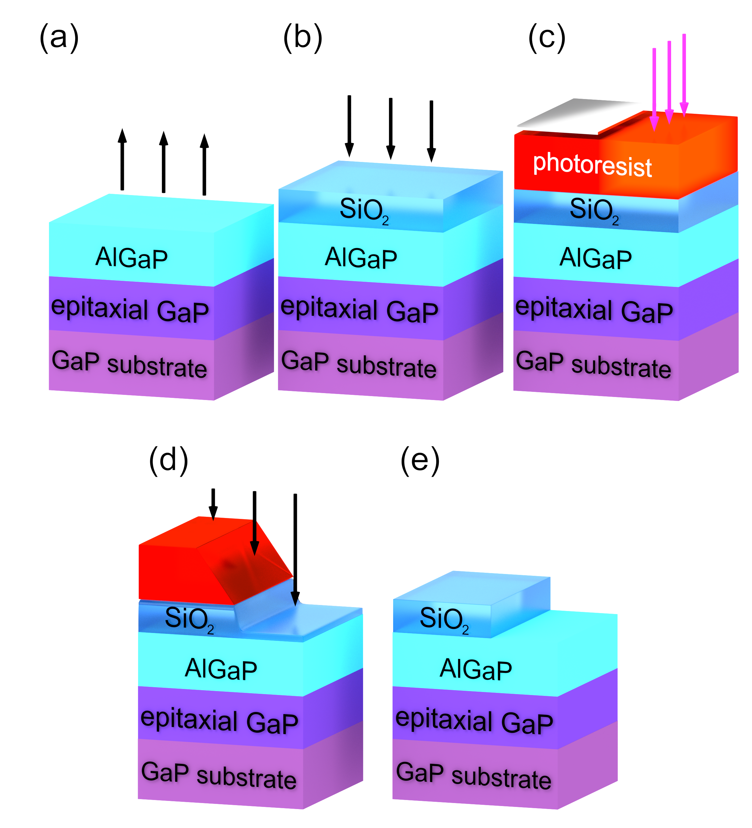
A SiO2 hard mask was employed for the etching experiments on both the GaP and AlGaP samples. Starting with a quarter GaP wafer and a quarter wafer of each AlGaP composition, of SiO2 were deposited by plasma-enhanced chemical vapor deposition (PECVD) in an Oxford Plasmalab 100 system with SiH4 and N2O as precursors. The SiO2 was then photolithographically patterned using the positive resist AZ6612 (Microchemicals GmbH) and a CF4/Ar RIE process in an Oxford NGP 80 system. The photoresist was subsequently removed using acetone, isopropanol, and an oxygen plasma (GIGAbatch 310 M from PVA TePla), which should also eliminate non-volatile etch residues originating from the CF4-containing RIE process. Finally, the GaP and AlGaP quarter wafers were diced into 3.5-mm 3.5-mm chips. The complete process flow is schematically illustrated in figure 1.
2.2 Etching
For the development of the selective ICP-RIE process with SiCl4 and SF6, the samples were etched for in an Oxford Instruments PlasmaPro 100 ICP system. The samples were placed side by side at the center of a 4-inch Si carrier wafer with no additional thermal conduction promoter such as oil, wax, or grease. The temperature of the carrier wafer was held at with a helium backing flow. The other process parameters were determined by the design of experiments (see below).
Following etching, the surface profile of the samples was measured with a Bruker DekTak XT profilometer, where the measured step height included the residual SiO2 hard mask. The hard mask was then stripped with a 90-s dip in buffered hydrofluoric acid (BHF), after which the etch profile was remeasured to determine both the etch rate and how much of the hard mask had been removed during the ICP-RIE process. The etch rate of GaP and AlGaP (x = 0.03 and x = 0.10) in BHF is negligible (measured to be for x = 0.10 by atomic force microscopy in a separate control experiment using an organic resist for the mask). If it was found that the SiO2 layer had been completely consumed during dry etching, the experiment was repeated for an etch duration of . To account for differences in the etch rate across the chip, the profile was measured at three positions from the edge towards the center in steps of and the results averaged.
2.3 Design of Experiments
Given the large parameter space of an ICP-RIE process [11], it is obviously time-consuming and laborious to analyze the process by investigating changes of one parameter at a time. To obtain a general understanding of the etch process more efficiently, i.e. without performing experiments for every possible parameter combination, we used a design-of-experiments (DOE) approach [22], probing a limited selection of points distributed over the parameter space. Specifically, a fractional factorial design comprising 24 experiments was created with the commercial statistical software JMP® (SAS Institute) [25]. We investigated the influence of the ICP power (), the chamber pressure (), the DC bias voltage (), and the SiCl4-to-SF6 ratio expressed as the fraction of SiCl4 () on the etch rate of GaP and the selectivity between GaP and AlGaP. The parameters of the individual experiments performed as specified by JMP for an I-optimality criterion [22] are displayed in table 1. An I-optimal design was possible because preliminary experiments gave us confidence in having already obtained a general understanding of the effect of the process conditions, and it provides for better prediction than e.g. the D-optimal design [22]. Values for the ICP power, pressure, and DC bias were chosen by the software from a continuous range. The chamber pressure was varied between and and the ICP power between and . The DC bias was set to values in the range of to by adjusting the RF power for each experiment individually. For , six explicit values were chosen according to preliminary experiments, keeping the combined total flow of SiCl4 and SF6 constant at .
-
No.
3 Results and Analysis
The etch rates obtained from the 24 experiments comprising the DOE are presented in table 1. The results were analyzed separately with respect to two responses: the GaP etch rate and the selectivity between GaP and AlGaP. Because the observed etch rates span several orders of magnitude and the error is expected to increase with both etch rate and selectivity, the least-squares regression analyses with JMP were performed on the common logarithm of the response (either etch rate or selectivity). Much better fits to the data were thus achieved; a systematic skew of the distribution of residuals as a function of the response was observed with a linear scale but not with a logarithmic scale.
To find an accurate model of minimal complexity, we started in each case by describing the desired response as an over-specified polynomial function of the process parameters, including cross terms. The coefficient of determination R2, the adjusted R2, and the probability value for both individual terms and the model as a whole were calculated. Terms with low statistical significance as gauged by a high -value were sequentially removed until the highest remaining individual -value was below 0.05 and removal of any more terms would lead to a substantial drop in the adjusted R2. The global maximum of the response within the explored parameter range was also determined as well as the variation of the response in the vicinity of the global maximum as a function of each process parameter individually.
3.1 GaP etch rate
We first present a model for the GaP etch rate alone. (Selectivity is treated with a separate model to account for the additional mechanisms in effect in the etching of AlGaP that do not pertain to GaP.) We restrict the model to processes for which the fraction of SiCl4 is within the range of 37.5% to 100% because the abrupt change from the low etch rates observed at lower fractions of SiCl4 would require a high-degree polynomial with more terms than can be justified with the size of the data set. In other words, we model a region of the parameter space for which GaP is etched at an appreciable rate. In addition, experiment 14 was excluded, as residues formed on this sample during the etch process leading to micromasking effects, so the etch rate could not be unambiguously determined.
After thorough investigation of various alternative polynomial functions of the process parameters, we consistently found that only the three terms listed in table 2 are necessary to provide a suitable model. The calculated dependence of the GaP etch rate on each individual process parameter with the others fixed at the value that gives the maximum response is displayed in figure 2. The ICP power dependence is not shown because this parameter is not statistically significant over the parameter range investigated, a result that suggests that the plasma is already saturated at the lowest value of with those species involved in the etching of GaP.
-
Term
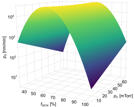
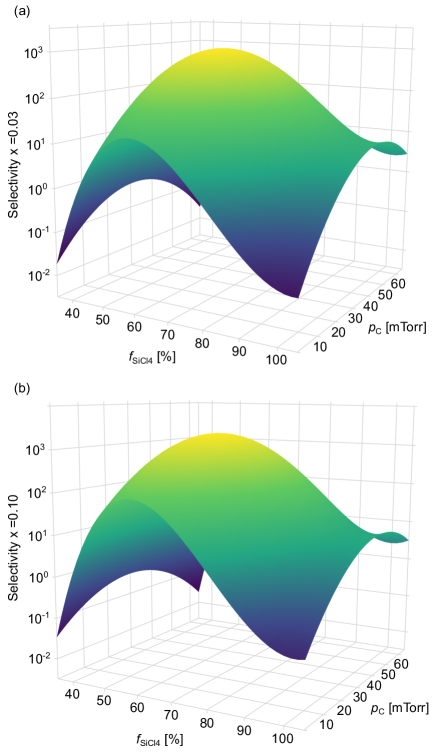
While the chamber pressure alone is also not significant, it does play a role in conjunction with the fraction of SiCl4. Indeed, it is not surprising that the product of pressure and SiCl4 fraction () appears in the model, as this term is related not only to the relative but also the absolute concentration of the etchants. The effect of is primarily to shift the value of for which the maximum etch rate is achieved, not to increase the etch rate, as is evident from figure 2(a), in which the modest monotonic increase in etch rate with pressure stays within the 95% confidence interval. The model predicts that for high SiCl4 content a higher pressure is preferable, whereas at high SF6 content a lower pressure yields a higher etch rate. This behavior is evident in the response surface plot in figure 3.
We interpret this finding as indicating that species originating from SiCl4 rather than SF6 dominate chemical reaction with GaP. Specifically, etching by ion bombardment of the surface is more important when the amount of chlorine-containing species is low, as this physical process should benefit from lower pressure. If the content of chlorine-containing species in the plasma is high, chemical reactions with the surface play a greater role and should be enhanced at high ion density, i.e. at high pressure.
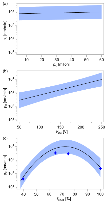
Of considerably more statistical significance is the DC bias. The monotonic increase in etch rate over one and a half orders of magnitude as the DC bias increases from to (figure 2(b)) is attributed to the change in kinetic energy of the ions bombarding the sample and the consequent enhancement of the physical component of etching. We note that the calculated optimum value for corresponds to one end of the parameter range investigated. It might therefore be possible to achieve an even higher etch rate if the parameter range is extended.
The third and statistically most significant term is the quadratic dependence on , which reflects the existence of an optimum ratio of SiCl4 to SF6 for achieving a high GaP etch rate (figure 2(c)). Individual experiments conducted within the scope of the DOE with a low fraction of SiCl4 had a very low etch rate, and processes containing only fluorine species showed virtually no etching, indicating that either SF6 is not a good etchant or it passivates the surface. On the other hand, the etch rate also declines at high SiCl4 content. Indeed, the etch rate for a plasma using only SiCl4 is one and half orders of magnitude lower than the optimum etch rate. Clearly, species originating from SF6 play a role in accelerating the etching despite the fact that a plasma using SF6 alone hardly etches GaP at all.
Over the range of parameters investigated, the model predicts a maximum GaP etch rate of at , , and , with the lower bound of the 95% confidence interval at and the upper bound at . To test the model’s capability to predict the etch rate with respect to , additional etch experiments were performed on GaP samples at flows of (), (), () and () for SiCl4 (SF6) with , , and . A high ICP power was chosen to ensure the saturation of dissociated and ionized species in the plasma. Although the observed etch rates are somewhat lower than predicted (figure 2(c)) (presumably because the additional runs were carried out at a later date than the DOE experiments and the environment in the ICP-RIE chamber may be slightly different), the results are within or near the 95% confidence interval of the fit and follow the shape of the curve nicely.
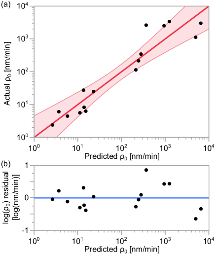
The quality of the model can be summarized in an actual-by-predicted plot, in which the experimentally observed etch rates are compared with those calculated from the model (figure 4). The coefficient of determination and the probability value indicate a good fit and a high statistical significance of the model.
3.2 Selectivity
Applying the same DOE analysis method to the selectivity for etching GaP versus AlGaP for the stoichiometries x = 0.03 and x = 0.10, we again consider only those experiments for which the fraction of SiCl4 is within the range of 37.5% to 100% and exclude those samples that exhibited micromasking, namely samples 4, 14, 15, 23, and 24. In this case, we find a considerably more complicated dependence on the various process parameters (table 3). Despite the relatively large number of terms, all but two -values are under 0.001, and the -value for the model as a whole is below 0.0001 for both stoichiometries, indicating quite high statistical significance.
-
Term )
The model predicts a maximum selectivity over the parameter range investigated of roughly 15000:1 for the x = 0.03 stoichiometry at , , , and = 63%, and 17000:1 for the x = 0.10 stoichiometry at , , , and , as is evident from figure 5. Such selectivity values are beyond the range measurable in our experiments using a -thick SiO2 hard mask. Figure 5 also shows the calculated dependence of the selectivity on each individual process parameter with the others fixed at the value that gives the maximum response. The selectivity behavior is qualitatively the same for the two AlGaP stoichiometries.
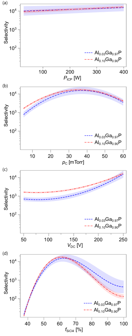
In contrast to the model for the GaP etch rate, the ICP power is statistically significant in determining the selectivity (figure 5(a)). Still, it plays the least important role. The modest gain in selectivity with ICP power, which is linear on this logarithmic scale, remains within or close to the 95% confidence interval. Again, the ICP power is expected to influence primarily the chemical component of the etching process, and the weak dependence suggests that the plasma composition is already close to being saturated at the lowest value of also for those species involved in the etching of AlGaP and not just GaP.
The influence of chamber pressure on selectivity (figure 5(b)) is also different than the situation for the GaP etch rate; several terms containing are statistically significant. The selectivity varies over an order of magnitude for the higher aluminum content and even more for the lower aluminum content. In both cases, the selectivity reaches a maximum in the middle of the pressure range evaluated. Since pressure is statistically insignificant in determining the GaP etch rate, this implies that there is some trade-off governing the AlGaP etch rate and suggests that, in addition to physical and chemical etching of the surface, other effects such as passivation may play a role. The interdependence of pressure and SiCl4 fraction is illustrated in the response surface plots in figure 6.
For DC bias (figure 5(c)), selectivity appears to be determined by an interplay between the GaP etch rate and the AlGaP etch rate, both of which are affected by this parameter. Hence, a quadratic dependence is observed in addition to an overall monotonic increase in selectivity with DC bias. Keeping with the hypothesis of a competition between chemical and physical processes, we attribute the nearly flat selectivity at low DC bias to a relatively weak contribution of the physical component which varies similarly for all stoichiometries. However, with increasing DC bias, the kinetic energy of the impinging ions accelerates the etching of GaP much more than the etching of AlGaP. This behavior is consistent with passivation primarily of AlGaP.
As was the case for the GaP etch rate, the fraction of SiCl4 has the most complex influence on the selectivity (figure 5(d)). The dependence is however not just quadratic now but includes linear and cubic terms. The result is a selectivity that peaks at a lower value of than the GaP etch rate and that plateaus at high values where the SF6 flow is low. This would again be consistent with preferential passivation of AlGaP, but where the passivation is provided specifically by the SF6. At high SF6 content, i.e. low values, both GaP and AlGaP are etched slowly and selectivity is low because SF6 is a poor etchant even for GaP. With increasing fraction of SiCl4, GaP starts to etch while AlGaP is passivated. At even higher values of , either the passivation mechanism becomes less effective for AlGaP or the plasma composition becomes less reactive or both, and selectivity begins declining even before the GaP etch rate peaks. The plateau at the highest values of is then ascribed to a limiting situation where the differentiation between GaP and AlGaP is no longer changing due to passivation or plasma reactivity.
Overall, the stoichiometry with 10% aluminum content yields a higher selectivity than the 3% composition, except in a portion of parameter space where the fraction of SiCl4 is high. As can be seen in figure 5(d), the selectivity is higher for x = 0.10 at its maximum but drops faster with increasing than the selectivity for x = 0.03. This suggest that, in addition to the passivation of AlGaP by SF6, there may be a competing enhancement at higher aluminum content of etching by chlorine species.
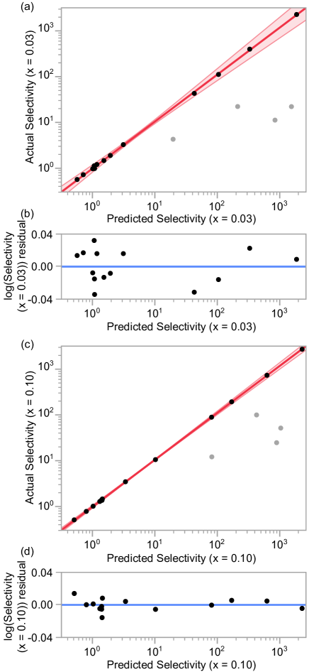
The actual-by-predicted plots for selectivity (figure 7) indicate that the model describes the observations well. For both x = 0.03 and x = 0.10, the coefficient of determination is and the probability value is . We attribute the higher value of R2 for selectivity in comparison to that for the GaP etch rate to the fact that the GaP and AlGaP samples were etched side by side for each parameter set, which may somewhat reduce any scatter due to run-to-run variations.
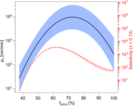
With the set of parameters that gives the maximum selectivity, the model for the GaP etch rate predicts an etch rate of with the lower bound of the 95% confidence interval at and the upper bound at . On the other hand, the process with the highest predicted GaP etch rate yields a selectivity of 2400:1 with the lower and upper bound of the 95% confidence interval at 1300:1 and 4300:1, respectively, for x = 0.03. For x = 0.10, the selectivity is predicted to be 1900:1 with the lower and upper bound of the 95% confidence interval at 1500:1 and 2300:1, respectively. The process can therefore be adjusted depending on whether high selectivity or high etch rate is required. The two models can be combined in a plot that shows both GaP etch rate and selectivity as a function of for the specific values of , and (figure 8), from which it is again apparent that the maximum etch rate occurs at a lower fraction of SiCl4 than the maximum selectivity.
Finally, we note that even higher selectivities may be attainable with aluminum contents greater than those tested here. From a practical point of view, epitaxial growth of AlGaP on a GaP substrate with an aluminum content well above 50% is entirely feasible, as the lattice mismatch between GaP and AlP is only 0.01% [26].
3.3 Surface Morphology
The surface morphology of the etched samples varies greatly over the range of process parameters used. Most of the deeply etched GaP samples have a smooth horizontal top surface without any evidence of residues being deposited. Only samples etched in processes 5, 9 and 14 show micromasking to various extents. In both experiment 9 and experiment 14, the fraction of SiCl4 is at the threshold between the passivating domain and the etching domain, so the micromasking may be related to the onset of passivation. The sample for process 5 exhibits micromasking only locally. In contrast, all of the samples that were not significantly etched exhibited some residue formation.
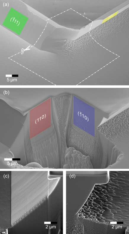
The etch profile can depend strongly on crystal lattice orientation. Figure 9 shows SEM micrographs of a sample that was etched under conditions for which the GaP etch rate and selectivity are both high (, , , and ). Here, we examined a square, 100- 100-, test feature aligned with the and the flats of the GaP wafer. This allows us to determine the orientation of the crystal lattice planes in the etch profile. Figure 9(a) displays a micrograph of one corner of the square, whereas figures 9(b) - (d) show the same structure after milling the corner along the dashed white line in figure 9(a) with a gallium focused ion beam (FIB). The colorized overlays in figures 9(a) and (b) indicate the orientation of the respective lattice planes. The process produces a smooth horizontal top surface as well as smooth, angled and somewhat curved sidewalls which converge to and planes in figures 9(c) and (d), respectively. This behavior is typical of chemical etching of III-V materials, for which etching of the densely packed, group-III-terminated planes are often slowest to etch. [27, 28]
4 Discussion
Literature on etching GaP selectively over AlGaP is scarce. The only other previously published method is a dry etching process that makes use of SiF4 and SiCl4 and etches GaP at with a selectivity of 124:1 with respect to Al0.6Ga0.4P [20]. We have observed similar behavior in an ICP-RIE process with CF4 and Cl2 [29]. Etching with a mixture of SiCl4 and SF6 has never before been investigated. However, selective dry-etching of GaAs in the presence of AlGaAs has been repeatedly reported using etching mixtures such as SF6/SiCl4 [30], CCl2F2 [31, 32, 33, 34] and SF6/BCl3 [13]. Selectivity in both the GaAs/AlGaAs system and the GaP/AlGaP system has been attributed to the formation of AlF3 on the surface of the aluminum-containing material which inhibits further etching [20, 30]. The passivating effect apparently arises from the much lower volatility of AlF3 compared to that of both AlCl3 and GaCl3 (table 4). Formation of GaF3, which also has low volatility, is not observed on GaAs or AlGaAs and is presumed to be impeded by a high kinetic barrier to reaction [30, 35], explaining why fluorine-containing species provide selectivity but not chlorine species. In the case of the phosphides, Epple et al verified the presence of an aluminum/fluorine-based layer on Al0.6Ga0.4P by Auger electron spectroscopy after etching with SiF4 and SiCl4 [20]. Our models for both the GaP etch rate and the selectivity are fully consistent with the above interpretation. We see evidence for strong surface passivation of AlGaP as compared to GaP, where the passivation is associated with SF6.
-
Product
Although the results of Epple et al and those presented here demonstrate that fluorine precursors alone, be it SiF4 or SF6, do not etch GaP, our results indicate that the etching reaction is not simply controlled by the SiCl4; the presence of some SF6 greatly enhances the etch rate (see figure 2(c)). Similar behavior has been observed both for the GaAs/AlGaAs system [30] and for GaN [35] when etching with SF6 and SiCl4, although it is not as dramatic. One contributing factor may be the rate of removal of the group V element, as argued by Karouta et al [35] for etching of GaN. The group V halides all have relatively low boiling or sublimation temperatures (table 4), but the temperatures for the fluorides are lower. PF3, PF5, and NF3 are especially volatile, evaporating well below room temperature. Thus, even though chlorine species may be primarily responsible for etching, fluorine atoms may contribute to the etch process, particularly in the absence of aluminum. It should be noted though that, if volatility of the reaction products were the only decisive factor, removal of gallium would become rate limiting. The effect of facile removal of phosphorous must therefore be to lower the reaction barrier to form the gallium containing products.
But this explanation alone is not sufficient. We need to account for our etch rates and selectivity being orders of magnitude higher with a mixture of SF6 and SiCl4 than those previously published for etching with SiF4 and SiCl4. We believe the relative strength with which sulfur and silicon bind fluorine and chlorine may instead be responsible. Table 5 lists bond dissociation energies for a series of silicon and sulfur halide molecules. Although we do not know what species are present in the plasma, and there may be a variety of both ions and radicals generated, it is nevertheless clear that fluorine is much more strongly bound to silicon than chlorine, and both halogen atoms are much more weakly bound to sulfur than to silicon. The use of SF6 instead of SiF4 may thus lead to a transfer of fluorine atoms to silicon but not chlorine atoms to sulfur. The result would be an increase in reactive chlorine species impinging on the surface to be etched. In fact, during etching of GaAs, Salimian et al [30] detected an increase in chlorine atoms in emission spectra when SF6 was added to SiCl4 plasmas. A related explanation has been proposed to describe etching of GaN with SiCl4/SF6/Ar chemistry [35].
-
Bond
The net result is that both the rate for etching GaP and the selectivity are strongly dependent on the ratio for SF6 to SiCl4 and the maximum values are reached when both gases are present. We note though that a proper analysis would need to take into account activation energies and the corresponding reaction barriers.
5 Conclusions
We successfully demonstrated highly selective etching of GaP in the presence of AlGaP with a plasma combining SF6 and SiCl4. A design of experiments implemented to model the parameter space yielded a predicted maximum selectivity of 15000:1 or more for etching of GaP over AlGaP with an Al content as low as 3% while simultaneously achieving GaP etch rates of several thousand . For the parameters tested, selectivities of up to 2700:1 and GaP etch rates above were measured experimentally. These results contrast with the previous work using SiF4 and SiCl4 claiming the need for high aluminum content in order to form an etch stop layer and for which etch rates and selectivity were two orders of magnitude lower. Use of a mixture of SiCl4 and SF6 instead of a purely chlorine-based plasma is essential for amplifying the GaP etch rate, which we predict can be tuned to values approaching . Although these high-etch-rate and high-selectivity processes exhibit a crystal orientation-dependent morphology, we believe that it may be possible to find less aggressive conditions suitable for pattern transfer applications while maintaining sufficient selectivity. With this advancement in the state of the art of GaP etching, new processing schemes become possible, such as those involving bonding of GaP onto carrier substrates. This opens the door to a variety of new GaP-based integrated nanophotonic applications.
Acknowledgments
This work was supported by funding from the European Union’s Horizon 2020 Programme for Research and Innovation under grant agreement No. 722923 (Marie Curie H2020-ETN OMT) and grant agreement No. 732894 (FET Proactive HOT).
References
References
- [1] M Kneissl et al. Advances in group III-nitride-based deep UV light-emitting diode technology. Semiconductor Science and Technology, 26(1):014036, 2010.
- [2] M H Chang, D Das, P V Varde, and M Pecht. Light emitting diodes reliability review. Microelectronics Reliability, 52(5):762–782, 2012.
- [3] F A Kish et al. Very high-efficiency semiconductor wafer-bonded transparent-substrate light-emitting diodes. Applied Physics Letters, 64(21):2839–2841, 1994.
- [4] F A Ponce and D P Bour. Nitride-based semiconductors for blue and green light-emitting devices. Nature, 386(6623):351–359, 1997.
- [5] M Yamaguchi, T Takamoto, K Araki, and N Ekins-Daukes. Multi-junction III–V solar cells: current status and future potential. Solar Energy, 79(1):78–85, 2005.
- [6] A W Bett, F Dimroth, G Stollwerck, and O V Sulima. III–V compounds for solar cell applications. Applied Physics A, 69(2):119–129, 1999.
- [7] A W Fang, H Park, O Cohen, R Jones, M J Paniccia, and J E Bowers. Electrically pumped hybrid AlGaInAs-silicon evanescent laser. Optics express, 14(20):9203–9210, 2006.
- [8] P Dong, T-C Hu, T-Y Liow, Y-K Chen, C Xie, X Luo, G-Q Lo, R Kopf, and A Tate. Novel integration technique for silicon/III–V hybrid laser. Optics express, 22(22):26854–26861, 2014.
- [9] D L Mathine. The integration of III–V optoelectronics with silicon circuitry. IEEE Journal of Selected Topics in Quantum Electronics, 3(3):952–959, 1997.
- [10] T E Kazior, R Chelakara, W Hoke, J Bettencourt, T Palacios, and H S Lee. High performance mixed signal and rf circuits enabled by the direct monolithic heterogeneous integration of GaN HEMTs and Si CMOS on a silicon substrate. In Compound Semiconductor Integrated Circuit Symposium (CSICS), 2011 IEEE, pages 1–4. IEEE, 2011.
- [11] S J Pearton. Reactive ion etching of III–V semiconductors. International Journal of Modern Physics B, 8(14):1781–1876, 1994.
- [12] M Shearn, X Sun, M D Henry, A Yariv, and A Scherer. Advanced plasma processing: etching, deposition, and wafer bonding techniques for semiconductor applications. Intech, 2010.
- [13] J W Lee, M W Devre, B H Reelfs, D Johnson, J N Sasserath, F Clayton, D Hays, and S J Pearton. Advanced selective dry etching of GaAs/AlGaAs in high density inductively coupled plasmas. Journal of Vacuum Science & Technology A: Vacuum, Surfaces, and Films, 18(4):1220–1224, 2000.
- [14] F Karouta, B Jacobs, O Schoen, and M Heuken. Chemical and complementary role of fluorine in a chlorine-based reactive ion etching of GaN. physica status solidi (a), 176(1):755–758, 1999.
- [15] M Volatier, D Duchesne, R Morandotti, R Ares, and V Aimez. Extremely high aspect ratio GaAs and GaAs/AlGaAs nanowaveguides fabricated using chlorine ICP etching with N2-promoted passivation. Nanotechnology, 21(13):134014, 2010.
- [16] T Maeda, J W Lee, R J Shul, J Han, J Hong, E S Lambers, S J Pearton, C R Abernathy, and W S Hobson. Inductively coupled plasma etching of III–V semiconductors in BCl3-based chemistries: I. GaAs, GaN, GaP, GaSb and AlGaAs. Applied surface science, 143(1):174–182, 1999.
- [17] T Maeda, J W Lee, R J Shul, J Han, J Hong, E S Lambers, S J Pearton, C R Abernathy, and W S Hobson. Inductively coupled plasma etching of III–V semiconductors in BCl3-based chemistries: II. InP, InGaAs, InGaAsP, InAs and AlInAs. Applied surface science, 143(1):183–190, 1999.
- [18] H Hahn, J B Gruis, N Ketteniss, F Urbain, H Kalisch, and A Vescan. Influence of mask material and process parameters on etch angle in a chlorine-based GaN dry etch. Journal of Vacuum Science & Technology A: Vacuum, Surfaces, and Films, 30(5):051302, 2012.
- [19] J W Lee, C J Santana, C R Abernathy, S J Pearton, and F Ren. Wet chemical etch solutions for AlGaP. Journal of the Electrochemical Society, 143(1):L1–L3, 1996.
- [20] J H Epple, C Sanchez, T Chung, K Y Cheng, and K C Hsieh. Dry etching of GaP with emphasis on selective etching over AlGaP. Journal of Vacuum Science & Technology B: Microelectronics and Nanometer Structures Processing, Measurement, and Phenomena, 20(6):2252–2255, 2002.
- [21] K Schneider, P Welter, Y Baumgartner, S Hönl, H Hahn, L Czornomaz, and P Seidler. Optomechanics with one-dimensional gallium phosphide photonic crystal cavities. In Quantum Nanophotonics, volume 10359, page 103590K. International Society for Optics and Photonics, 2017.
- [22] R H Myers, D C Montgomery, and C M Anderson-Cook. Response surface methodology: process and product optimization using designed experiments. John Wiley & Sons, 2016.
- [23] L Ilzarbe, MJ Álvarez, E Viles, and M Tanco. Practical applications of design of experiments in the field of engineering: a bibliographical review. Quality and Reliability Engineering International, 24(4):417–428, 2008.
- [24] R A Fisher. The design of experiments. Oliver And Boyd; Edinburgh; London, 1937.
- [25] SAS Institute Inc., Cary, NC. JMP®, Version 13.1.0., 1989-2007.
- [26] A Addamiano. X-ray data for the phosphides of aluminium, gallium and indium. Acta Crystallographica, 13(6):505–505, 1960.
- [27] H C Gatos and M C Lavine. Characteristics of the 111 surfaces of the III–V intermetallic compounds. Journal of the Electrochemical Society, 107(5):427–433, 1960.
- [28] Y Tarui, Y Komiya, and Y Harada. Preferential etching and etched profile of GaAs. Journal of The Electrochemical Society, 118(1):118–122, 1971.
- [29] K Schneider, P Welter, Y Baumgartner, H Hahn, L Czornomaz, and P Seidler. Gallium phosphide-on-silicon dioxide photonic devices. Journal of Lightwave Technology, under review.
- [30] S Salimian and C B Cooper III. Selective dry etching of GaAs over AlGaAs in SF6/SiCl4 mixtures. Journal of Vacuum Science & Technology B: Microelectronics Processing and Phenomena, 6(6):1641–1644, 1988.
- [31] K L Seaward, N J Moll, D J Coulman, and W F Stickle. An analytical study of etch and etch-stop reactions for GaAs on AlGaAs in CCl2F2 plasma. Journal of applied physics, 61(6):2358–2364, 1987.
- [32] C M Knoedler and T F Kuech. Selective GaAs/AlGaAs reactive ion etching using CCl2F2. Journal of Vacuum Science & Technology B: Microelectronics Processing and Phenomena, 4(5):1233–1236, 1986.
- [33] J Vatus, J Chevrier, P Delescluse, and J-F Rochette. Highly selective reactive ion etching applied to the fabrication of low-noise algaas gaas fet’s. IEEE Transactions on Electron Devices, 33(7):934–937, 1986.
- [34] K Hikosaka, T Mimura, and K Joshin. Selective dry etching of AlGaAs-GaAs heterojunction. Japanese Journal of Applied Physics, 20(11):L847, 1981.
- [35] F Karouta, B Jacobs, P Vreugdewater, N G H van Melick, O Schoen, H Protzmann, and M Heuken. High etch rate and smooth morphology using a novel chemistry in reactive ion etching of GaN. Electrochemical and solid-state letters, 2(5):240–241, 1999.
- [36] D R Linde, editor. CRC Handbook of Chemistry and Physics. CRC Press, 84th edition, 6 2003.
- [37] R Walsh. Bond dissociation energy values in silicon-containing compounds and some of their implications. Accounts of Chemical Research, 14(8):246–252, 1981.
- [38] B D Gailbreath, C A Pommerening, S M Bachrach, and L S Sunderlin. Potential energy surface of SCl. The Journal of Physical Chemistry A, 104(13):2958–2961, 2000.