peter.wiecha@cemes.fr, vincent.paillard@cemes.fr 22institutetext: ICB, Université de Bourgogne-Franche Comté, CNRS, Dijon, France 33institutetext: LAAS, Université de Toulouse, CNRS, Toulouse, France 44institutetext: CEA-LETI, Université Grenoble-Alpes, MINATEC Campus, Grenoble, France 55institutetext: LTM, Université Grenoble-Alpes, CNRS, Grenoble, France
Fano-Resonances in High Index Dielectric Nanowires for Directional Scattering
Abstract
High refractive index dielectric nanostructures provide original optical properties thanks to the occurrence of size- and shape-dependent optical resonance modes. These modes commonly present a spectral overlap of broad, low-order modes (e.g. dipolar modes) and much narrower, higher-order modes. The latter are usually characterized by a rapidly varying frequency-dependent phase, which – in superposition with the lower order mode of approximately constant phase – leads to typical spectral features known as Fano resonances. Interestingly, such Fano resonances occur in dielectric nanostructures of the simplest shapes. In spheroidal nanoparticles, interference between broad magnetic dipole and narrower electric dipole modes can be observed. In high aspect-ratio structures like nanowires, either the electric or the magnetic dipolar mode (depending on the illumination conditions) interferes with higher order multipole contributions of the same nature (electric or magnetic). Using the analytical Mie theory, we analyze the occurrence of Fano resonances in high-index dielectric nanowires and discuss their consequences like unidirectional scattering. By means of numerical simulations, we furthermore study the impact on those Fano resonances of the shape of the nanowire cross-sections as well as the coupling of two parallel nanowires. The presented results show that all-dielectric nanostructures, even of simple shapes, provide a reliable low-loss alternative to plasmonic nanoantennas.
0.1 Introduction
Research on effects of light-matter interaction occurring at subwavelength dimensions has been drawing increasing attention during the last three decades. When we talk about subwavelength dimensions, at visible and near-infrared frequencies, we find ourselves at the nanometer scale, a length-scale particularly interesting with regards to applications in information processing and optical computing, single molecule sensing or biomedicine, amongst many other domains. Most applications rely on the possibility to strongly confine far-field radiation to deeply subwavelength small volumes at resonant modes of specifically designed nanoparticles. Resonances are either due to surface plasmons in the case of metals (field of plasmonics) or to constructive optical interference in the case of dielectrics. Usually, all phenomena can be described by classical electrodynamics, i.e. by the set of Maxwell’s equations maxwell_dynamical_1865 .
In the following, we will briefly describe the fields of plasmonic and high index dielectric nanostructures, with a particular attention on their specificity and main differences.
Then, in the other sections of this chapter, we will give an overview on Fano Resonances in dielectric nanostructures, with an emphasis on directional scattering as a result of Fano-like interference phenomena. In particular, we will present the so-called Kerker’s conditions under which unidirectional scattering occurs in dielectric spherical particles and extend the idea to cylinders. To substantiate the findings on dielectric nanowires, we will compare experimental results to Mie theory and numerical simulations.
Finally, we analyze the directional scattering behavior of nanowires with nonsymmetric cross-sections, as well as the case of a system of two coupled nanowires.
0.1.1 Plasmonics
One of the main driving forces in nano-optics is the field of plasmonics muhlschlegel_resonant_2005 ; maier_plasmonics_2010 . Electromagnetic waves impinging on metals launch collective oscillations of the free electrons in the conduction band of the metal. The dielectric constant of metals is negative, leading to an imaginary wave vector. Fields are therefore evanescent and confined within a small region at the surface, called the skin-depth. In consequence, the collective oscillations of the electrons propagate along the surface and are therefore called surface plasmon polaritons (SPP). In small metallic particles, the propagation of SPPs is hindered due to the spatial confinement and localized modes appear, so-called localized surface plasmon resonances (LSP).
These confined plasmon oscillations allow to squeeze light into tiny volumes of subwavelength size, far below the diffraction limit and yield extremely high local field enhancements schuck_improving_2005 . In the visible spectral range, this results in sizes of several tenths to a few hundreds of nanometers for resonant metallic nanostructures. Such plasmonic particles are often referred to as optical (nano-)antennas muhlschlegel_resonant_2005 .
In the context on this chapter, we would like to mention a few selected examples for applications of plasmonic nanostructures. Beyond the possibility to obtain strong localized field intensities, plasmonic nanoantennas can be designed to provide directional scattering. This can be achieved for instance by tailoring plasmonic geometries which provide a simultaneous electric and magnetic response yao_controlling_2016 . With complex structures like bimetallic antennas, wavelength selective directional color routing can be obtained from individual nanoantennas shegai_bimetallic_2011 . Also the directional emission of quantum emitters can be controlled using plasmonic antennas bonod_ultracompact_2010 ; curto_unidirectional_2010 ; hancu_multipolar_2014 . For an extensive introduction on plasmonics, see e.g. reference maier_plasmonics_2010 .
0.1.2 High Refractive Index Dielectric Nano-Particles
The focus of this chapter lies on a different kind of nano-antennas than the plasmonic ones. Recently, dielectric nanostructures of high refractive index started drawing a lot of attention as promising alternatives to metallic particles, since they offer in a similar way tailorable optical resonances kuznetsov_optically_2016 .
Even in very simple systems such as nanospheres kuznetsov_magnetic_2012 , or cylindrical cao_tuning_2010 ; kallel_tunable_2012 or rectangular nanowires (NWs) ee_shape-dependent_2015 , optical resonance modes can be tuned over (and beyond) the whole visible spectral range. Flexible tailoring of the resonant behavior can be achieved using dielectric nanostructures of more complex shapes wiecha_evolutionary_2017 .
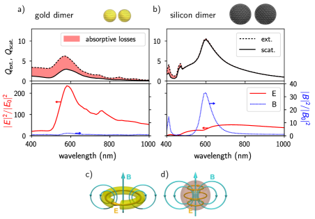
A particular advantage of dielectric particles over metallic ones are their very low losses albella_electric_2014 ; caldarola_non-plasmonic_2015 ; decker_resonant_2016 . This property is directly related to the generally low imaginary part of the dielectric function for wavelengths above the direct bandgap. It is demonstrated in the upper spectra of figure 1(a-b), where a gold and a silicon dimer are compared in terms of scattering efficiency and dissipation. Although the electric field-enhancement (as well as the confinement) is usually at least an order of magnitude lower than for plasmonic antennas (see also Fig. 1(a-b), lower spectra), the reduced dissipative losses are a tremendous advantage and can be a decisive factor in applications such as field enhanced spectroscopy wells_silicon_2012 ; regmi_all-dielectric_2016 .
Another unique feature of dielectric nanoparticles is the possibility to obtain strong magnetic resonances from geometries as simple as a sphere garcia-etxarri_strong_2011 ; ginn_realizing_2012 ; evlyukhin_demonstration_2012 ; valuckas_direct_2017 . In contrast, plasmonics require complex geometries to obtain important magnetic resonances kuznetsov_magnetic_2012 (see figure 1c and 1d). These magnetic-type resonances allow also to obtain a strong enhancement of the magnetic near-field, which is usually significantly more intense than the magnetic field intensity obtainable using metal nanostructures albella_electric_2014 ; bakker_magnetic_2015 ; mirzaei_electric_2015 (see figure 1(a-b), bottom spectra). The magnetic resonances of dielectric nanostructures can be exploited to enhance the decay rate of magnetic dipole transitions rolly_promoting_2012 ; schmidt_dielectric_2012 ; baranov_modifying_2017 ; wiecha_decay_2017 . While the optical magnetic near-field and the magnetic contribution to the local density of photonic states (LDOS) in the vicinity of nanostructures can be probed using appropriate SNOM tips (gold-ring coated tips for sensing the -field devaux_local_2000 ; burresi_probing_2009 ; tips prepared with rare-earth-ion doped nano-crystals, e.g. using Eu3+, for the magnetic LDOS aigouy_mapping_2014 ; carminati_electromagnetic_2015 ), it is experimentally far more demanding to access the intrinsic field enhancement. While no measurement was reported in the visible regime, strong magnetic field enhancement in dielectric cylinders has recently been experimentally demonstrated at THZ frequencies kapitanova_giant_2017 .
0.1.3 General Applications of Dielectric Nano-Structures
High-index dielectric nanostructures are increasingly used in many nano-optical applications, often – but not exclusively – as alternatives to their lossy plasmonic equivalent.
In perfect analogy to plasmonics, it is possible to design color filters wood_all-dielectric_2017 and (color) holograms zhao_full-color_2016 ; li_dielectric_2017-1 or to use dielectric nano-structures for “color-printing” at the diffraction limit proust_all-dielectric_2016 ; flauraud_silicon_2017 .
Field-enhanced spectroscopy can even more benefit by replacing plasmonic-based substrates with dielectric nanoantenna-based substrates for two main reasons. The first reason is the prevention of the reabsorption of the generated fluorescence or Raman signal that occurs in the metal nanostructures gerard_strong_2008 ; wells_silicon_2012 ; caldarola_non-plasmonic_2015 ; regmi_all-dielectric_2016 ; cambiasso_bridging_2017 . The second reason is that heat generation can be almost completely suppressed using dielectric nanoantennas, while plasmonic structures suffer from strong local heating albella_low-loss_2013 ; albella_electric_2014 . This point is important to realize very sensitive biosensors bontempi_highly_2017 , as a slight increase of temperature can be fatal for fragile biomolecules or simply decrease the luminescence intensity.
Further applications of photonic nano-particles based on dielectric materials can be found in photovoltaics: The geometrical structure of the photovoltaic junction can be shaped such that its absorption covers optimally the solar spectrum. It has been shown that already simple geometries like nano-blocks or nanowires can significantly improve the absorptive coverage of the solar spectrum, compared to two-dimensional layers used in commercial photovoltaic cells cao_semiconductor_2010 ; kallel_enhanced_2013 . A different approach is to design dielectric (low-loss) nano-antennas able to trap and redirect the incoming solar light towards the classical (planar) photovoltaic junction brongersma_light_2014 ; priolo_silicon_2014 .
Finally, the strong field enhancements occurring at the resonant modes of dielectric nanostructures can be used to promote nonlinear optical effects. For instance, it has been shown that surface second harmonic generation (SHG) can be strongly enhanced in dielectric nanoparticles wiecha_enhanced_2015 ; wiecha_origin_2016 ; liu_resonantly_2016 ; cambiasso_bridging_2017 . Also the third harmonic generation (THG) can be significantly enhanced shcherbakov_enhanced_2014 ; melik-gaykazyan_third-harmonic_2017 and its emission can be tailored shcherbakov_nonlinear_2015 ; wang_shaping_2017 in silicon nano-particles, by making use of their magnetic resonances. Even ultrafast all-optical switching of the optical transmission has been demonstrated using silicon nano-discs shcherbakov_ultrafast_2015 .
0.2 Fano Resonances and Kerker’s Conditions
Fano resonances occur due to the interference between two scattering amplitudes, when a resonant state energetically lies in a background of continuous states. If the scattering amplitudes of the resonance and the background are of comparable magnitude, the cross section of the Fano resonance follows a very characteristic, asymmetric lineshape. Although Ugo Fano originally considered the interference between a single state with a continuum fano_effects_1961 , very similar resonance profiles occur if a narrow resonant state interferes with a significantly broader state. Such interference between two resonant states of similar amplitude but different linewidths are nowadays often colloquially called Fano resonances. The Fano lineshape can be written as
| (1) |
with the reduced energy
| (2) |
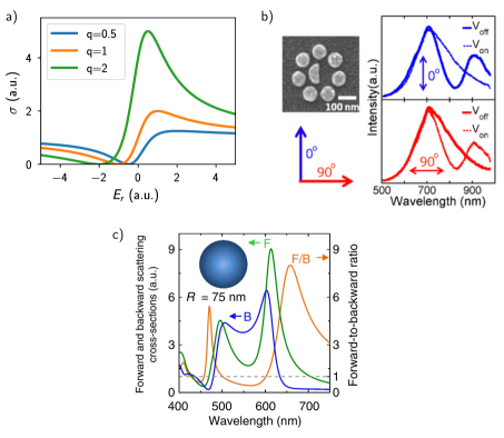
where is the position of the resonance and it’s spectral width. The amplitude of the background state(s) is considered constant over the spectral range of the Fano profile. is called the Fano parameter, which corresponds to the ratio between the resonance amplitude and the non-resonant background. Note that in the limit of a very strong resonance on a weak background, equation (1) converges towards a Lorentzian. On the other hand, for a strong interference between the resonance and the background exists, which results in the typical line shapes. The cases , , and are shown in figure 2a.
For a detailed coupled mode theory of Fano resonances in optical resonators, see also reference fan_temporal_2003 .
0.2.1 Fano in nano-optics
Optical Fano resonances in photonic nanostructures allow to obtain anomalous, usually very sharp mode signatures in the scattering or extinction spectra. The most prominent structure geometry which pronounces Fano-like mode profiles is the class of oligomers: Ordered arrangements of several nano-particles. Tailorable Fano resonances have been observed for example in dielectric oligomers. The resonances occur as a result of an interference between the magnetic resonance of each individual constitute and a collective magnetic response of the entire system and can be tailored by the size and distance between the individual particles hopkins_interplay_2015 . Also in plasmonic oligomers Fano resonances occur, for instance due to interference between electric and magnetic modes bakhti_fano-like_2016 . Using an asymmetric arrangement of plasmonic particles, it is even possible to create an optical “Fano-switch” chang_plasmonic_2012 : Via the polarization of the incident light, the Fano resonance can be toggled on and off, as shown in figure 2b.
But Fano-like scattering profiles are not limited to complex geometrical arrangements like the above mentioned oligomers. In fact, Fano resonances occur in very simple systems such as individual, dielectric nanowires of rectangular cross-section with relatively high aspect-ratio. Narrow Fano lineshapes appear in the scattering spectra of such nanowires, at which the scattering rapidly drops, while absorption strongly rises. This can be explained by a spectrally sharp guided mode along the NW width, which interferes with a spectrally broad leaky mode resonance fan_optical_2014 . A similar kind of Fano resonance due to the interference between guided modes (along the NW axis) and Mie resonances has recently been described in short dielectric nanowires abujetas_high-contrast_2017 . For a detailed review on Fano resonances in photonics, we would like to point to reference limonov_fano_2017 .
0.2.2 Kerker’s Conditions at Optical Frequencies
A special type of Fano resonance was studied by Kerker et al. in hypothetical magneto-dielectric nanospheres, for which they found conditions at which exclusive forward (FW) or backward (BW) scattering occurs kerker_electromagnetic_1983 . Kerker et al. described two possible configurations, called the Kerker’s conditions. The first Kerker’s condition requires equal electric permittivity and magnetic permeability (), at which zero-backward scattering occurs. The second Kerker’s condition predicts zero-forward scattering in the case if the first order magnetic Mie coefficient and first order electric Mie coefficient are of equal value but of opposite sign ().
In contrast to particularly designed metamaterials pendry_controlling_2006 , no known material in nature has a direct response to rapidly oscillating magnetic fields. Hence, is unitary in dielectric nano-particles. However, equally strong electric and magnetic resonances can de-facto fulfill the first Kerker’s condition, if they overlap energetically gomez-medina_electric_2011 ; nieto-vesperinas_angle-suppressed_2011 . The second condition on the other hand contradicts the optical theorem and is therefore unphysical. Nevertheless, almost zero-forward scattering can still be achieved, however scattering efficiencies are in that case usually considerably lower compared to the first Kerker’s condition (zero-backward scattering) alu_how_2010 ; nieto-vesperinas_angle-suppressed_2011 ; wiecha_strongly_2017 .
Note that, although the Kerker’s conditions were originally derived for spherical particles, it has been shown later that they have their origin in a cylindrical symmetry and can hence be generalized to particles of cylindrical symmetry, excited along their long axis zambrana-puyalto_duality_2013 .
0.2.3 Directional Scattering From Nanoparticles
Directional Scattering from Nanospheres and Small Particles
The possibility to de facto fulfill the Kerker’s conditions at visible wavelengths for unidirectional forward and backward scattering has been first discussed around 2010 for spherical high refractive index dielectric nanoparticles (silicon or germanium) nieto-vesperinas_angle-suppressed_2011 ; garcia-etxarri_strong_2011 ; gomez-medina_electric_2011 . For instance, spectra showing the directional scattering of light from an individual silicon nanosphere are presented in figure 2c. It turned out that the directionality of light scattering occurs in many kinds of dielectric nanoparticles, like individual nanocubes or nanocube dimers campione_tailoring_2015 . It has been shown as well, that the luminescence of emitting dipoles placed near the surface of spherical dielectric nanoparticles can be focused in a preferred direction via simultaneous excitation of electric and magnetic modes in the spheres rolly_boosting_2012 . The same effect has been predicted for quantum emitters embedded inside dielectric nanodiscsrocco_controlling_2017 .
The experimental demonstration of Kerker-type scattering in the visible range was achieved about two years after the theoretical prediction. In early 2013, two research groups around Novotny and Luk’yanchuk published almost at the same time their results on exclusive forward or backward scattering from dielectric nanoparticles person_demonstration_2013 ; fu_directional_2013 . Since then, similar results have been achieved for different geometries of dielectric nanoparticles, like nanodiscs staude_tailoring_2013 , nanospheroids lukyanchuk_optimum_2015 or nanosphere dimers for switchable directional scattering albella_switchable_2015 ; yan_directional_2015 ; shibanuma_experimental_2017 .
The main insight of all these works is that dielectric spheres permit a spectral overlap of electric and magnetic dipolar resonances, thus allowing to effectively satisfy Kerker’s conditions and obtain a distinct directional scattering.
Directional Scattering from Nanowires
In a nanosphere excited with a linearly polarized plane wave, transverse electric (TE) and transverse magnetic (TM) polarizations are not separable, hence the according modes are always simultaneously excited. In the case of normally illuminated nanowires by the plane wave on the other hand, it is possible to excite either TE or TM modes by choosing an illumination with a polarization either perpendicular, or parallel, to the NW axis. In that case, it becomes impossible to obtain spectrally overlapping electric and magnetic resonances, so that Kerker’s conditions (for instance ) cannot be satisfied.
Several propositions have been made to overcome this limitation and generate Kerker-type directional scattering from nanowires (NWs) as well. For instance, by using hybrid plasmonic / dielectric materials in core-shell NWs, an electric / magnetic response can be tailored, leading to directional scattering liu_scattering_2013 (a concept which, by the way, has been successfully applied also to “non-wire” nano-particles guo_multipolar_2016 ). In this context it has been demonstrated that properly designed plasmonic / dielectric core-shell NWs can be even rendered invisible thanks to destructive interference between electric and magnetic modes liu_invisible_2015 . However, the implementation of plasmonic components would increase losses due to absorption in the metal, as well as the complexity of the object fabrication. In that regard, all-dielectric solutions seem advantageous. In analogy to metal/dielectric hybrid NWs, Kerker-type directional scattering can occur in NWs with a radially anisotropic refractive index liu_superscattering_2017 . Likewise, the invisibility effect can be achieved in multilayer all-dielectric NWs mirzaei_all-dielectric_2015 .
Directional Scattering from Complex Dielectric Nanostructures
Obviously, complex geometries can be used to tailor the spectral positions of electric and magnetic resonances. Without going in much detail, Let us refer to two examples as illustration.
First, it has been shown that V-shaped dielectric resonators can be designed for bidirectional color routing (in perpendicular directions with respect to the incidence). This directionality has been found to be a result of interference between electric dipolar, magnetic dipolar as well as an electric quadrupolar mode. Furthermore, the left/right color routing effect is observed in addition to the occurrence of an unidirectional forward / backward scattering li_all-dielectric_2016 .
As a second example for tailored scattering behavior, we would like to mention a study on semi-hollow nano-discs, i.e. nanorings in which the central hole goes not through the entire height. Such geometry allows to create a bianisotropic directional scattering, which is dependent on the illumination direction. In other words, light is scattered purely in forward direction, or not – depending on its incidence direction. These nanostructures could be used to design reflective metasurfaces, which is only possible thanks to the anisotropy of the individual metasurface unit-cells, inducing a phase shift in the reflected amplitude. Off resonance, the dielectric metasurface is transparent, which would be impossible using metallic mirrors, due to their high ohmic losses alaee_all-dielectric_2015 .
0.2.4 Applications of Nanoscale Directional Scattering
The last part of this section is dedicated to an overview on some useful applications of directional scattering by nanoscale particles.
We previously discussed the example of a dielectric metasurface as a lossless mirror, which can be also designed to offer an incidence-dependent reflectivity alaee_all-dielectric_2015 . Other all-dielectric metasurfaces have been proposed, offering a generalized Brewster effect for arbitrary angles and wavelengths paniagua-dominguez_generalized_2016 . Such metasurfaces are particularly promising for applications in photovoltaics: Light-trapping could significantly reduce reflective losses and increase the efficiency of state-of-the-art solar cells muskens_design_2008 ; spinelli_light_2014 ; priolo_silicon_2014 ; li_method_2015 ; mann_opportunities_2016 .
The possibility to render a nanowire completely invisible mirzaei_all-dielectric_2015 ; liu_invisible_2015 has been proposed as a tool to design invisible electric circuits fan_invisible_2012 .
Directional scattering of the radiation from quantum emitters by dielectric nano-particles has been theoretically predicted rolly_boosting_2012 ; rolly_controllable_2013 ; yang_controlling_2015 and recently also experimentally demonstrated peter_directional_2017 ; cihan_silicon_2017 . Together with the Purcell effect – the decay rate enhancement for emitters in the proximity of nano-structures purcell_spontaneous_1946 – the directionality in the emission renders dielectric particles and nanowires very promising for many applications in field enhanced spectroscopy. However, the position of the emitter with respect to the particle is crucial for the scattering directionality. This sensitivity to the emitter location holds generally, for quantum emitters outside rolly_crucial_2011 as well as for such embedded inside dielectric nano-particles rocco_controlling_2017 . On the other hand, this supposed drawback can be actually an advantage and might be used in far-field measurements to gain information about the emitter location on a subwavelength scale. Using Kerker-type scattering effects, the emission from a nanostructure itself, such as photoluminescence paniagua-dominguez_enhanced_2013 ; ramezani_hybrid_2015 ; brenny_directional_2016 or nonlinear effects like second harmonic generation carletti_shaping_2016 ; xiong_compact_2016 , can be focused into a preferred direction, which is useful in the detection of weak signals from individual nanostructures.
0.3 Mie Theory
In this section, we will explain Kerker-type directional scattering in the context of Mie theory for nanospheres and adapt the same idea in a slightly modified form to infinitely long cylinders (i.e. nanowires). The results are mainly excerpted from an earlier publication. Therefore, for more details see also wiecha_strongly_2017 .
Mie theory provides an analytical description of the response of spherical or cylindrical particles (with an infinitely long axis in the latter case) to an incident optical field. The far-field response to an external illumination is written as a multipole series whose coefficients – the “Mie scattering coefficients” and – can be regarded as weights for corresponding electric () and magnetic () multipole moments. The expressions “electric” and “magnetic” also refer to the fact that the magnetic, respectively electric field components, are zero in the scattering plane.
As a short remark we would like to mention that it has been demonstrated, that the Mie coefficients for a cylinder can be written equivalently as a series of Fano profiles, which is explained by the interference between the continuum of modes represented by the incident field and a (sharper) resonant mode (a Mie resonance of the cylinder) rybin_mie_2013 . Even though this is not directly linked to the demonstration below, it is an interesting interpretation of Mie resonances, adding a different viewpoint on them in general.
0.3.1 Directional Scattering from Spheres and Cylinders
Nanospheres
In the description of the light scattering in spherical particles (which is the “classical” Mie theory), all fields are expanded in vector spherical harmonics, leading to a kind of multipole development. Scattering to the far-field can be written using the scattering amplitude matrix (S-matrix), which connects the incident field with the scattered field bohren_absorption_1998
| (3) |
is the wavenumber, the scattered (outgoing) wave with the distance to the sphere center and is the incident plane wave. For simplicity, we will now assume that the sphere is sufficiently small, such that only the first order of the development has a significant magnitude. In this case the two nonzero S-matrix elements write bohren_absorption_1998 ; hosemann_computation_1971
| (4) | ||||
In Eq. (4), is the scattering angle with respect to the incident wave vector, and corresponds to the forward direction. This directly leads to the well-known conditions for exclusive BW or FW scattering:
| (5) | |||||
Nanowires
Infinitely long cylinders can also be treated using Mie theory by developing the fields in vector cylindrical harmonics. Under normal incidence, the Mie S-matrix writes in this case bohren_absorption_1998
| (6) |
is the wavenumber and the distance to the cylinder axis. As for nanospheres, we assume nanowires of sufficiently small diameter, such that only the lowest two orders significantly contribute to scattering, leading to
| (7) | ||||
Again, is the scattering angle with respect to the incident wave vector with the forward direction.
Under normal incidence, the transverse magnetic (TM) polarized components of the scattered field are proportional to the S-matrix component (respectively, the transverse electric (TE) components are proportional to ). According to Eqs. (7), scattering from a TE polarized normally incident plane wave ( NW axis) is only due to the “electric” multipole contributions . On the other hand, a TM polarized illumination ( NW axis) induces scattering exclusively via the “magnetic” Mie terms .
In perfect analogy to equation (5) we find
| (8) | ||||
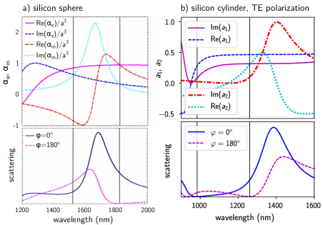
The same conditions hold for TE polarization with and the “electric” coefficients . The main difference to the case of a sphere is that we do not have an interference of dipolar electric and dipolar magnetic modes anymore, but an interference between dipolar and quadrupolar modes of the same, “electric” or “magnetic”, character, depending on the incident polarization. In the upper panels of figure 3, the Mie coefficients and for a silicon sphere (Fig. 3a) are compared to the coefficients and of a silicon nanowire as function of the wavelength. Indeed, the coefficients show very similar spectral dependencies, which holds equally for their amplitude and phase. Comparing the FW/BW scattering spectra of both geometries (bottom plots in figure 3), the similarity in Mie coefficients is reproduced. Please note also the Fano-like profiles in the scattering resonances, shown in figure 3: The interference of a spectrally narrow mode (electric mode for the sphere, “”-mode in the case of the nanowire) with a spectrally large “background-mode” (sphere: magnetic mode, nanowire: “”-mode) leads to the directional response and a Fano-like line shape.
We conclude that interference of multiple spectrally overlapping orders of either electric or magnetic modes in dielectric nanowires can lead to similar FW/BW scattering phenomena as interfering electric and magnetic dipole resonances in dielectric nano-spheres. Different behaviors, hence different directions of light scattering, could be addressed by incident light polarization.
0.3.2 Nanowires: Resonant Enhancement of the Electric and Magnetic Field
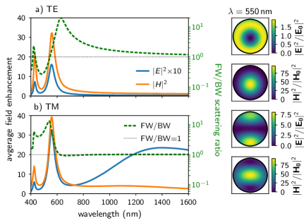
It is possible to expand the electromagnetic fields inside the cylinder in the same way as the scattered near- or far-field. For details, please refer to the textbook of Bohren and Huffmann bohren_absorption_1998 . In figure 4 we show the average field intensity enhancement inside a silicon NW (SiNW) of radius nm for illumination with (a) TE and (b) TM polarized plane waves, respectively. The silicon dispersion is taken from the book of Palik palik_silicon_1997 . At resonance, we observe for both the TE and for TM cases not only high electric field intensities (blue lines), but also a strong enhancement of the magnetic field (orange lines). The magnetic field increases even far stronger compared to the electric field intensity, an observation which is in agreement with recent experimental results from dielectric cylinders in the GHz regime kapitanova_giant_2017 . We conclude that a simultaneous excitation of strong electric and magnetic fields occurs in dielectric, non-magnetic (i.e. ) NWs, even under pure TE or TM polarized illumination and normal incidence. Hence, in analogy to the findings of Kerker et al., the observed directionality (dashed green lines in Fig. 4) can be interpreted as a result of the interference between “effective” electric and magnetic modes. In particular, at the non-degenerate, fundamental TM01 mode (nm), where only the internal electric field shows a resonant enhancement while the magnetic field intensity follows a flat line beyond nm (see Fig. 4b), no directional scattering is obtained. This is also the case for any small diameter nanowire supporting the fundamental resonant mode only. For illustration the electric and magnetic field intensity patterns inside the NW are shown on the right of Fig. 4 at nm.
0.3.3 Nanowires: Multipolar Contributions to Directional Scattering
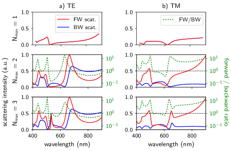
Previously, we used only the two first coefficients of the field expansion. We want to assess if this approximation remains valid for larger NWs, and how many orders of multipole contributions are necessary to describe with a sufficient agreement the directional scattering phenomena. Let us illustrate this empirically by taking a SiNW of radius nm for example. Since directional scattering is a result of the interference between multiple simultaneously excited modes, the FW/BW resolved scattered intensity cannot be plotted individually for the different contributing scattering coefficients and (for TE and TM polarized, normal incidence, respectively). In figure 5, the FW and BW scattered intensity from a normally illuminated SiNW (nm) is calculated successively for an increasing number of contributing terms. Figure 5a shows the scattering under TE polarized illumination, Fig. 5b the TM case. We have shown elsewhere wiecha_strongly_2017 that for a NW of nm radius, terms higher than the first two orders are negligible. Yet, even for a larger NW as shown in Fig. 5, the response is mostly determined by the first two orders of the Mie series, while only few additional features arise if third order modes are considered as well. In conclusion, despite some missing spectral features, using only the first two Mie orders gives already a very good approximation even in the case of large dielectric NWs.
0.4 Directional Scattering from Silicon Nanowires
In this section, we present experiments performed on silicon nanowires showing the directional scattering phenomenon as function of size and shape. We compare the experimental data to Mie theory and numerical simulations, confirming the accuracy of the predictions. Having confirmed the validity of our approach, we analyze theoretically a more sophisticated system of two normally illuminated parallel nanowires, lying on a plane. We find that such a system can be used to switch the scattering direction between forward and backward, simply by changing the distance between the two wires.
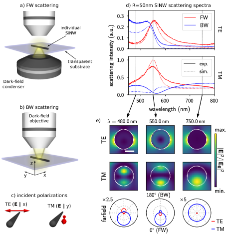
0.4.1 Cylindrical Nanowires
We start with the simplest possible geometry: A cylindrical SiNW in vacuum. The SiNWs are VLS grown dhalluin_silicon_2010 and dispersed on a transparent silica substrate with lithographic markers, so the exactly same NW can be examined on different experimental setups. We perform standard dark field microscopy either in reflection (BW scattering) or in transmission geometry (FW scattering). The measurement setup is schematically shown in Fig. 6a and 6b for FW and BW scattering, respectively. Details on the technique are described elsewhere wiecha_strongly_2017 . The incident light is polarized either perpendicular (TE) or along the NW axis (TM), as illustrated in Fig. 6c. We use the scattering from small cylindrical nanowires (nm) for normalization of the FW and BW spectra: In sufficiently small NWs only the fundamental dipolar TM01 mode is excited, which results in an omni-directional scattering (corresponding to a dipolar source along the NW axis, as explained in the previous section). We hence assume that the FW and BW scattered intensities are of equal strength and normalize all spectra using this reference. We compare our experimental results to Mie theory and 2D simulations by the Green dyadic method (“GDM”, assuming structures of infinite length along martin_generalized_1995 ; paulus_greens_2001 ). The GDM simulations reproduce Mie with almost perfect agreement (see also wiecha_strongly_2017 ).
Results of the scattering experiments on a SiNW of radius nm are shown in Fig. 6d for TE (top) and TM (bottom) illumination. In the case of TE polarized illumination FW scattering occurs for large wavelengths (nm), while BW scattering takes over at shorter wavelengths (nm). In the TM case on the other hand, FW scattering dominates over the whole accessible spectral range, however with a pronounced peak around nm, where a maximum of scattered FW intensity coincides with a minimum in BW scattering. Near-field plots and corresponding far-field scattering patterns are shown in figure 6e (top and bottom, respectively) for selected wavelengths, indicated by dashed black lines in figure 6d. Note that around nm, we obtain the possibility to invert the main scattering direction by simply flipping the polarization from TM to TE (see also Fig. 6e, bottom left). Via the NW diameter, this spectral zone can be tuned to other frequencies. At longer wavelengths (nm), only the nondegenerate TM01 mode exists, leading to very weak overall scattering under TE incidence and to the aforementioned, omnidirectional radiation pattern in the TM geometry. Interestingly, while it is possible to induce directional BW scattering in the TE configuration, under TM illumination BW scattering is generally very weak and mainly FW scattering occurs – with the exception of a uniform scattering when only the TM01 mode is excited.
In summary, we note that although we do observe BW scattering (mainly under TE polarization) it mostly remains weak compared to the FW scattered light. In the case of TM polarized illumination, the FW/BW scattering ratio is even almost exclusively .
0.4.2 Rectangular Nanowires
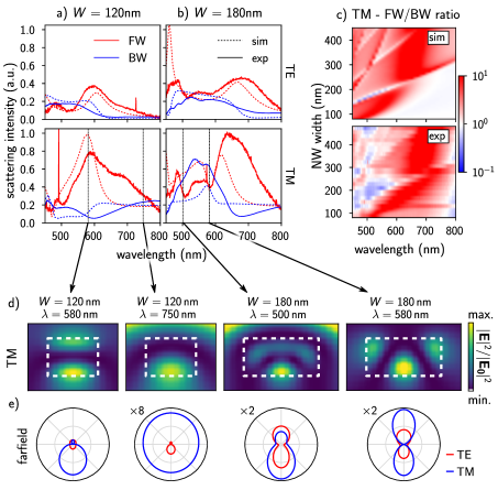
In a second step we analyze what happens if the cylindrical symmetry of the nanowire cross section is broken. We therefore fabricate SiNWs of rectangular section by electron beam lithography (EBL) and subsequent dry-etching han_realization_2011 ; guerfi_high_2013 on a silicon-on-quartz (SOQ) substrate moriceau_materials_2014 . A great advantage of our top-down approach on SOQ is the possibility to create silicon nanostructures of arbitrary shape by EBL on a transparent substrate from single crystalline silicon. Using this material rather than deposited polycrystalline or amorphous silicon guarantees that the best optical properties of single crystal silicon are kept. Defined by the thickness of the silicon layer on the SOQ substrate (nm), the height of the rectangular nanowires is constant. The rectangular section is varied by changing the SiNWs width. The length µm is chosen large compared to the focal spot of the illuminating optics in order to obtain a purely Mie-like response traviss_antenna_2015 . All NWs have excellent surface properties, low roughness and steep flanks, verified by scanning electron microscopy.
The results of our systematic FW/BW scattering measurements are shown in figure 7c (for TM polarization). Selected spectra for SiNWs of width nm and nm are shown in figure 7a-b, respectively, where TE polarized illumination is shown in the top, the TM case in the bottom plot. The comparison of experiments with GDM simulations shows a very good agreement. Having a look at the FW/BW ratios (Fig. 7c, TM polarization) we observe that mostly forward scattering occurs. This is similar to our observations on cylindrical SiNWs. Figure 7d and e) finally show selected simulated near-field plots and far-field scattering patterns for TM polarized illumination. In particular, the first two panels in Fig. 7d-e show, for a NW of nearly symmetric section, the excitation of the first strongly directional mode (corresponding to TE01/TM11) and the region of omnidirectional scattering in the red spectrum (corresponding to TE01/TM11), which are almost identically found as in cylindrical NWs.
Under TM excitation, we observe branches of a kind of Fano resonance, which do not occur in cylindrical NWs: In narrow spectral zones, the FW/BW ratio is almost unity (see Fig. 7b around nm and Fig. 7c, white diagonal branches). In a confined spectral window the otherwise strong forward scattering is suddenly suppressed, while BW scattering increases. Resonances with such field profiles are observed neither under TE polarization, nor in symmetric SiNWs (see also wiecha_strongly_2017 ). These sharp features are a result of horizontal guided modes along the SiNW width (-direction, in the NW cross-sectional plane) and their interference with the leaky “background” mode of, in comparison, large spectral width. The wire side facets act as the Fabry-Perot cavity mirrors and the nanowire slab has an effective index of () for the supported guided mode in the case of TM polarized illumination at nm. With this effective index, a standing wave pattern with three lobes matches perfectly a nanowire width of nm, in nice agreement to the wavelength and width at which the resonance occurs. The calculated near-field pattern (very right panel of figure 7d) finally confirms the presence of a guided mode. We verified the guided mode assumption also for the other branches in figure 7c, at each of which the NW width corresponds to an odd integer multiple of half the wavelength divided by the effective index. A standing-wave pattern of increased order can be found at these positions in the near-field plots. We note that former studies on scattering from rectangular dielectric NWs used Fabry-Perot modes, reflected between the side-walls of the wire, for the analytical description of the scattering fan_optical_2014 ; landreman_fabry-perot_2016 .
0.4.3 Coupled Nanowires
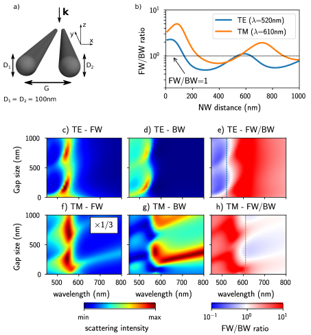
Finally we analyze a system composed of two identical, parallel silicon nanowires illuminated normally with respect to the plane defined by their axes, as schematically shown in Fig. 8a. The radius of the wires is nm, (c.f. also figure 6), the incident plane wave is polarized either perpendicular (TE) or parallel to the wire axis (TM). Using the GDM, the scattered intensity is calculated in forward and backward direction. The results are shown in Fig. 8 as function of the incident wavelength and polarization as well as the distance between the NWs, also labeled “gap” .
Figs. 8c-e show c) forward, d) backward scattering and e) the FW/BW ratio in the case of TE polarization. Figs. 8f-h show the same for the TM case. We find a strong modulation of the scattering, which is in agreement with former observations in the total scattering signal mirzaei_electric_2015 . Interestingly, not only the scattering intensity itself shows a modulation of high contrast; likewise, the FW/BW ratio shows a significant dependence on the distance between the two SiNWs. Figure 8b shows the FW/BW scattering ratio for TE (blue dashed line) and TM polarization (orange dashed line) at two fixed wavelengths of particularly strong contrast in the scattering signal. Obviously, at selected wavelengths, it is possible to toggle between mainly forward, isotropic, and mainly backward scattering simply by varying the gap size between the two nanowires. Furthermore, an interesting feature of coupled nanowires is to increase the scattering efficiency either in forward or backward direction, compared to the case of a single nanowire where it is rather low at Kerker’s conditions shibanuma_unidirectional_2016 . This is due to the fact that Kerker’s conditions are usually fulfilled out of a resonance. This observation opens perspectives for several applications in sensing or field-enhanced spectroscopy by realizing more efficient directional dielectric nanoantennas. We could for instance imagine two parallel dielectric nanowires embedded in a flexible transparent matrix for sub-wavelength optical distance measurements at visible frequencies.
Conclusion and Outlook
We compared plasmonics with the emerging field of high-index dielectric nanostructures and gave an overview about the recent research in nano-optics on directional scattering at the single particle level. We introduced the Kerker’s conditions, their representation for nonmagnetic materials at visible frequencies, and put them in the context of Fano resonances in general. Furthermore, we compared the conditions for unidirectional scattering in Mie theory for spherical particles and cylindrical nanowires. We experimentally demonstrated directional scattering first in the “Mie case” of cylindrical silicon nanowires, where we found the possibility to switch between forward and backward scattering by a simple rotation of the incident polarization. Subsequently, we studied the effects of an asymmetric nanowire shape. For rectangular NWs of increasing height/width aspect-ratio, we observed the apparition of Fano-like modes due to the occurrence of spectrally sharp guided modes along the NW width. Finally, we theoretically studied a system of two coupled SiNWs and found that such an arrangement allows to toggle between FW and BW scattering, simply by adjusting the distance between the coupled wires. Optical Fano resonances in nanostructures open perspectives for light management and guiding at the nanometer scale, for sub diffraction-limited optical sensing or for applications in field-enhanced spectroscopies
References
- [1] J. Clerk Maxwell. A Dynamical Theory of the Electromagnetic Field. Philosophical Transactions of the Royal Society of London, 155:459–512, 1865.
- [2] P. Mühlschlegel, H.-J. Eisler, O. J. F. Martin, B. Hecht, and D. W. Pohl. Resonant Optical Antennas. Science, 308(5728):1607–1609, June 2005.
- [3] S.A. Maier. Plasmonics: Fundamentals and Applications. Springer US, 2010.
- [4] P. J. Schuck, D. P. Fromm, A. Sundaramurthy, G. S. Kino, and W. E. Moerner. Improving the Mismatch between Light and Nanoscale Objects with Gold Bowtie Nanoantennas. Physical Review Letters, 94(1):017402, January 2005.
- [5] Kan Yao and Yongmin Liu. Controlling Electric and Magnetic Resonances for Ultracompact Nanoantennas with Tunable Directionality. ACS Photonics, May 2016.
- [6] Timur Shegai, Si Chen, Vladimir D. Miljković, Gülis Zengin, Peter Johansson, and Mikael Käll. A bimetallic nanoantenna for directional colour routing. Nature Communications, 2:ncomms1490, September 2011.
- [7] Nicolas Bonod, Alexis Devilez, Brice Rolly, Sebastien Bidault, and Brian Stout. Ultracompact and unidirectional metallic antennas. Physical Review B, 82(11):115429, September 2010.
- [8] Alberto G. Curto, Giorgio Volpe, Tim H. Taminiau, Mark P. Kreuzer, Romain Quidant, and Niek F. van Hulst. Unidirectional Emission of a Quantum Dot Coupled to a Nanoantenna. Science, 329(5994):930–933, August 2010. 00954.
- [9] Ion M. Hancu, Alberto G. Curto, Marta Castro-López, Martin Kuttge, and Niek F. van Hulst. Multipolar Interference for Directed Light Emission. Nano Letters, 14(1):166–171, January 2014.
- [10] Arseniy I. Kuznetsov, Andrey E. Miroshnichenko, Mark L. Brongersma, Yuri S. Kivshar, and Boris Luk’yanchuk. Optically resonant dielectric nanostructures. Science, 354(6314), November 2016.
- [11] Arseniy I. Kuznetsov, Andrey E. Miroshnichenko, Yuan Hsing Fu, JingBo Zhang, and Boris Luk’yanchuk. Magnetic light. Scientific Reports, 2:492, July 2012.
- [12] Linyou Cao, Pengyu Fan, Edward S. Barnard, Ana M. Brown, and Mark L. Brongersma. Tuning the Color of Silicon Nanostructures. Nano Letters, 10(7):2649–2654, July 2010.
- [13] Houssem Kallel, Arnaud Arbouet, Gérard BenAssayag, Abdallah Chehaidar, Alexis Potié, Bassem Salem, Thierry Baron, and Vincent Paillard. Tunable enhancement of light absorption and scattering in Si(1-x)Ge(x) nanowires. Physical Review B, 86(8):085318, August 2012.
- [14] Ho-Seok Ee, Ju-Hyung Kang, Mark L. Brongersma, and Min-Kyo Seo. Shape-Dependent Light Scattering Properties of Subwavelength Silicon Nanoblocks. Nano Letters, 15(3):1759–1765, March 2015.
- [15] Peter R. Wiecha, Arnaud Arbouet, Christian Girard, Aurélie Lecestre, Guilhem Larrieu, and Vincent Paillard. Evolutionary multi-objective optimization of colour pixels based on dielectric nanoantennas. Nature Nanotechnology, 12(2):163–169, February 2017. 00002.
- [16] Pablo Albella, Rodrigo Alcaraz de la Osa, Fernando Moreno, and Stefan A. Maier. Electric and Magnetic Field Enhancement with Ultralow Heat Radiation Dielectric Nanoantennas: Considerations for Surface-Enhanced Spectroscopies. ACS Photonics, 1(6):524–529, June 2014.
- [17] Martín Caldarola, Pablo Albella, Emiliano Cortés, Mohsen Rahmani, Tyler Roschuk, Gustavo Grinblat, Rupert F. Oulton, Andrea V. Bragas, and Stefan A. Maier. Non-plasmonic nanoantennas for surface enhanced spectroscopies with ultra-low heat conversion. Nature Communications, 6:7915, August 2015.
- [18] Manuel Decker and Isabelle Staude. Resonant dielectric nanostructures: A low-loss platform for functional nanophotonics. Journal of Optics, 18(10):103001, 2016.
- [19] Sabrina M. Wells, Igor A. Merkulov, Ivan I. Kravchenko, Nickolay V. Lavrik, and Michael J. Sepaniak. Silicon Nanopillars for Field-Enhanced Surface Spectroscopy. ACS Nano, 6(4):2948–2959, April 2012. 00052.
- [20] Raju Regmi, Johann Berthelot, Pamina M. Winkler, Mathieu Mivelle, Julien Proust, Frédéric Bedu, Igor Ozerov, Thomas Begou, Julien Lumeau, Hervé Rigneault, María F. García-Parajó, Sébastien Bidault, Jérôme Wenger, and Nicolas Bonod. All-Dielectric Silicon Nanogap Antennas To Enhance the Fluorescence of Single Molecules. Nano Letters, 16(8):5143–5151, August 2016.
- [21] A. García-Etxarri, R. Gómez-Medina, L. S. Froufe-Pérez, C. López, L. Chantada, F. Scheffold, J. Aizpurua, M. Nieto-Vesperinas, and J. J. Sáenz. Strong magnetic response of submicron Silicon particles in the infrared. Optics Express, 19(6):4815, March 2011.
- [22] James C. Ginn, Igal Brener, David W. Peters, Joel R. Wendt, Jeffrey O. Stevens, Paul F. Hines, Lorena I. Basilio, Larry K. Warne, Jon F. Ihlefeld, Paul G. Clem, and Michael B. Sinclair. Realizing Optical Magnetism from Dielectric Metamaterials. Physical Review Letters, 108(9):097402, February 2012.
- [23] Andrey B. Evlyukhin, Sergey M. Novikov, Urs Zywietz, René Lynge Eriksen, Carsten Reinhardt, Sergey I. Bozhevolnyi, and Boris N. Chichkov. Demonstration of Magnetic Dipole Resonances of Dielectric Nanospheres in the Visible Region. Nano Letters, 12(7):3749–3755, July 2012.
- [24] Vytautas Valuckas, Ramón Paniagua-Domínguez, Yuan Hsing Fu, Boris Luk’yanchuk, and Arseniy I. Kuznetsov. Direct observation of resonance scattering patterns in single silicon nanoparticles. Applied Physics Letters, 110(9):091108, 2017. 00000.
- [25] Reuben M. Bakker, Dmitry Permyakov, Ye Feng Yu, Dmitry Markovich, Ramón Paniagua-Domínguez, Leonard Gonzaga, Anton Samusev, Yuri Kivshar, Boris Luk’yanchuk, and Arseniy I. Kuznetsov. Magnetic and Electric Hotspots with Silicon Nanodimers. Nano Letters, 15(3):2137–2142, March 2015.
- [26] Ali Mirzaei and Andrey E. Miroshnichenko. Electric and magnetic hotspots in dielectric nanowire dimers. Nanoscale, 7(14):5963–5968, March 2015.
- [27] Brice Rolly, Betina Bebey, Sebastien Bidault, Brian Stout, and Nicolas Bonod. Promoting magnetic dipolar transition in trivalent lanthanide ions with lossless Mie resonances. Physical Review B, 85(24):245432, June 2012.
- [28] M. K. Schmidt, R. Esteban, J. J. Sáenz, I. Suárez-Lacalle, S. Mackowski, and J. Aizpurua. Dielectric antennas - a suitable platform for controlling magnetic dipolar emission. Optics Express, 20(13):13636, June 2012.
- [29] Denis G. Baranov, Roman S. Savelev, Sergey V. Li, Alexander E. Krasnok, and Andrea Alù. Modifying magnetic dipole spontaneous emission with nanophotonic structures. Laser & Photonics Reviews, 11(3):1600268–n/a, 2017.
- [30] Peter R. Wiecha, Arnaud Arbouet, Aurélien Cuche, Vincent Paillard, and Christian Girard. Decay Rate of Magnetic Dipoles near Non-magnetic Nanostructures. arXiv:1707.07006 [cond-mat, physics:physics], July 2017.
- [31] Eloïse Devaux, Alain Dereux, Eric Bourillot, Jean-Claude Weeber, Yvon Lacroute, Jean-Pierre Goudonnet, and Christian Girard. Local detection of the optical magnetic field in the near zone of dielectric samples. Physical Review B, 62(15):10504–10514, October 2000.
- [32] M. Burresi, D. van Oosten, T. Kampfrath, H. Schoenmaker, R. Heideman, A. Leinse, and L. Kuipers. Probing the Magnetic Field of Light at Optical Frequencies. Science, 326(5952):550–553, October 2009.
- [33] L. Aigouy, A. Cazé, P. Gredin, M. Mortier, and R. Carminati. Mapping and Quantifying Electric and Magnetic Dipole Luminescence at the Nanoscale. Physical Review Letters, 113(7):076101, August 2014. 00035.
- [34] R. Carminati, A. Cazé, D. Cao, F. Peragut, V. Krachmalnicoff, R. Pierrat, and Y. De Wilde. Electromagnetic density of states in complex plasmonic systems. Surface Science Reports, 70(1):1–41, March 2015. 00040.
- [35] Polina Kapitanova, Vladimir Ternovski, Andrey Miroshnichenko, Nikita Pavlov, Pavel Belov, Yuri Kivshar, and Michael Tribelsky. Giant field enhancement in high-index dielectric subwavelength particles. Scientific Reports, 7(1):731, April 2017. 00001.
- [36] Thomas Wood, Meher Naffouti, Johann Berthelot, Thomas David, Jean-Benoît Claude, Léo Métayer, Anne Delobbe, Luc Favre, Antoine Ronda, Isabelle Berbezier, Nicolas Bonod, and Marco Abbarchi. All-Dielectric Color Filters Using SiGe-Based Mie Resonator Arrays. ACS Photonics, 4(4):873–883, April 2017.
- [37] Wenyu Zhao, Bingyi Liu, Huan Jiang, Jie Song, Yanbo Pei, and Yongyuan Jiang. Full-color hologram using spatial multiplexing of dielectric metasurface. Optics Letters, 41(1):147, January 2016.
- [38] Zile Li, Inki Kim, Lei Zhang, Muhammad Q. Mehmood, Muhammad S. Anwar, Murtaza Saleem, Dasol Lee, Ki Tae Nam, Shuang Zhang, Boris Luk’yanchuk, Yu Wang, Guoxing Zheng, Junsuk Rho, and Cheng-Wei Qiu. Dielectric Meta-Holograms Enabled with Dual Magnetic Resonances in Visible Light. ACS Nano, September 2017.
- [39] Julien Proust, Frédéric Bedu, Bruno Gallas, Igor Ozerov, and Nicolas Bonod. All-Dielectric Colored Metasurfaces with Silicon Mie Resonators. ACS Nano, 10(8):7761–7767, August 2016.
- [40] Valentin Flauraud, Miguel Reyes, Ramón Paniagua-Domínguez, Arseniy I. Kuznetsov, and Juergen Brugger. Silicon Nanostructures for Bright Field Full Color Prints. ACS Photonics, June 2017.
- [41] Davy Gérard, Jérôme Wenger, Alexis Devilez, David Gachet, Brian Stout, Nicolas Bonod, Evgeny Popov, and Hervé Rigneault. Strong electromagnetic confinement near dielectric microspheres to enhance single-molecule fluorescence. Optics Express, 16(19):15297, September 2008.
- [42] Javier Cambiasso, Gustavo Grinblat, Yi Li, Aliaksandra Rakovich, Emiliano Cortés, and Stefan A. Maier. Bridging the Gap between Dielectric Nanophotonics and the Visible Regime with Effectively Lossless Gallium Phosphide Antennas. Nano Letters, 17(2):1219–1225, February 2017. 00004.
- [43] Pablo Albella, M. Ameen Poyli, Mikolaj K. Schmidt, Stefan A. Maier, Fernando Moreno, Juan José Sáenz, and Javier Aizpurua. Low-Loss Electric and Magnetic Field-Enhanced Spectroscopy with Subwavelength Silicon Dimers. The Journal of Physical Chemistry C, 117(26):13573–13584, July 2013.
- [44] Nicolò Bontempi, Katie E. Chong, Henry W. Orton, Isabelle Staude, Duk-Yong Choi, Ivano Alessandri, Yuri S. Kivshar, and Dragomir N. Neshev. Highly sensitive biosensors based on all-dielectric nanoresonators. Nanoscale, 9(15):4972–4980, 2017. 00000.
- [45] Linyou Cao, Pengyu Fan, Alok P. Vasudev, Justin S. White, Zongfu Yu, Wenshan Cai, Jon A. Schuller, Shanhui Fan, and Mark L. Brongersma. Semiconductor Nanowire Optical Antenna Solar Absorbers. Nano Letters, 10(2):439–445, February 2010.
- [46] Houssem Kallel, Abdallah Chehaidar, Arnaud Arbouet, and Vincent Paillard. Enhanced absorption of solar light in Ge/Si core-sheath nanowires compared to Si/Ge core-sheath and Si1-xGex nanowires: A theoretical study. Journal of Applied Physics, 114(22):224312, December 2013.
- [47] Mark L. Brongersma, Yi Cui, and Shanhui Fan. Light management for photovoltaics using high-index nanostructures. Nature Materials, 13(5):451–460, May 2014. 00279.
- [48] Francesco Priolo, Tom Gregorkiewicz, Matteo Galli, and Thomas F. Krauss. Silicon nanostructures for photonics and photovoltaics. Nature Nanotechnology, 9(1):19–32, January 2014.
- [49] Peter R. Wiecha, Arnaud Arbouet, Houssem Kallel, Priyanka Periwal, Thierry Baron, and Vincent Paillard. Enhanced nonlinear optical response from individual silicon nanowires. Physical Review B, 91(12):121416, March 2015. 00000.
- [50] Peter R. Wiecha, Arnaud Arbouet, Christian Girard, Thierry Baron, and Vincent Paillard. Origin of second-harmonic generation from individual silicon nanowires. Physical Review B, 93(12):125421, March 2016. 00000.
- [51] Sheng Liu, Michael B. Sinclair, Sina Saravi, Gordon A. Keeler, Yuanmu Yang, John Reno, Gregory M. Peake, Frank Setzpfandt, Isabelle Staude, Thomas Pertsch, and Igal Brener. Resonantly Enhanced Second-Harmonic Generation Using III–V Semiconductor All-Dielectric Metasurfaces. Nano Letters, 16(9):5426–5432, September 2016.
- [52] Maxim R. Shcherbakov, Dragomir N. Neshev, Ben Hopkins, Alexander S. Shorokhov, Isabelle Staude, Elizaveta V. Melik-Gaykazyan, Manuel Decker, Alexander A. Ezhov, Andrey E. Miroshnichenko, Igal Brener, Andrey A. Fedyanin, and Yuri S. Kivshar. Enhanced Third-Harmonic Generation in Silicon Nanoparticles Driven by Magnetic Response. Nano Letters, 14(11):6488–6492, November 2014.
- [53] Elizaveta V. Melik-Gaykazyan, Maxim R. Shcherbakov, Alexander S. Shorokhov, Isabelle Staude, Igal Brener, Dragomir N. Neshev, Yuri S. Kivshar, and Andrey A. Fedyanin. Third-harmonic generation from Mie-type resonances of isolated all-dielectric nanoparticles. Phil. Trans. R. Soc. A, 375(2090):20160281, March 2017. 00000.
- [54] Maxim R. Shcherbakov, Alexander S. Shorokhov, Dragomir N. Neshev, Ben Hopkins, Isabelle Staude, Elizaveta V. Melik-Gaykazyan, Alexander A. Ezhov, Andrey E. Miroshnichenko, Igal Brener, Andrey A. Fedyanin, and Yuri S. Kivshar. Nonlinear Interference and Tailorable Third-Harmonic Generation from Dielectric Oligomers. ACS Photonics, 2(5):578–582, May 2015.
- [55] Lei Wang, Sergey Kruk, Lei Xu, Mohsen Rahmani, Daria Smirnova, Alexander Solntsev, Ivan Kravchenko, Dragomir Neshev, and Yuri Kivshar. Shaping the third-harmonic radiation from silicon nanodimers. Nanoscale, 9(6):2201–2206, February 2017. 00000.
- [56] Maxim R. Shcherbakov, Polina P. Vabishchevich, Alexander S. Shorokhov, Katie E. Chong, Duk-Yong Choi, Isabelle Staude, Andrey E. Miroshnichenko, Dragomir N. Neshev, Andrey A. Fedyanin, and Yuri S. Kivshar. Ultrafast All-Optical Switching with Magnetic Resonances in Nonlinear Dielectric Nanostructures. Nano Letters, 15(10):6985–6990, October 2015.
- [57] U. Fano. Effects of Configuration Interaction on Intensities and Phase Shifts. Physical Review, 124(6):1866–1878, December 1961.
- [58] Shanhui Fan, Wonjoo Suh, and J. D. Joannopoulos. Temporal coupled-mode theory for the Fano resonance in optical resonators. JOSA A, 20(3):569–572, March 2003.
- [59] Wei-Shun Chang, J. Britt Lassiter, Pattanawit Swanglap, Heidar Sobhani, Saumyakanti Khatua, Peter Nordlander, Naomi J. Halas, and Stephan Link. A Plasmonic Fano Switch. Nano Letters, 12(9):4977–4982, September 2012.
- [60] Yuan Hsing Fu, Arseniy I. Kuznetsov, Andrey E. Miroshnichenko, Ye Feng Yu, and Boris Luk’yanchuk. Directional visible light scattering by silicon nanoparticles. Nature Communications, 4:1527, February 2013.
- [61] Ben Hopkins, Dmitry S. Filonov, Andrey E. Miroshnichenko, Francesco Monticone, Andrea Alù, and Yuri S. Kivshar. Interplay of Magnetic Responses in All-Dielectric Oligomers To Realize Magnetic Fano Resonances. ACS Photonics, 2(6):724–729, 2015.
- [62] Saïd Bakhti, Alexandre V. Tishchenko, Xavier Zambrana-Puyalto, Nicolas Bonod, Scott D. Dhuey, P. James Schuck, Stefano Cabrini, Selim Alayoglu, and Nathalie Destouches. Fano-like resonance emerging from magnetic and electric plasmon mode coupling in small arrays of gold particles. Scientific Reports, 6:32061, September 2016.
- [63] Pengyu Fan, Zongfu Yu, Shanhui Fan, and Mark L. Brongersma. Optical Fano resonance of an individual semiconductor nanostructure. Nature Materials, 13(5):471–475, May 2014. 00072.
- [64] Diego R. Abujetas, Miguel A. G. Mandujano, Eugenio R. Méndez, and José A. Sánchez-Gil. High-Contrast Fano Resonances in Single Semiconductor Nanorods. ACS Photonics, 4(7):1814–1821, July 2017.
- [65] Mikhail F. Limonov, Mikhail V. Rybin, Alexander N. Poddubny, and Yuri S. Kivshar. Fano resonances in photonics. Nature Photonics, 11(9):543–554, September 2017.
- [66] M. Kerker, D.-S. Wang, and C. L. Giles. Electromagnetic scattering by magnetic spheres. Journal of the Optical Society of America, 73(6):765, June 1983.
- [67] J. B. Pendry, D. Schurig, and D. R. Smith. Controlling Electromagnetic Fields. Science, 312(5781):1780–1782, June 2006.
- [68] Raquel Gómez-Medina, Braulio García-Cámara, Irene Suárez-Lacalle, Francisco González, Fernando Moreno, Manuel Nieto-Vesperinas, and Juan José Sáenz. Electric and magnetic dipolar response of germanium nanospheres: Interference effects, scattering anisotropy, and optical forces. Journal of Nanophotonics, 5(1):053512–053512–9, 2011. 00000.
- [69] M. Nieto-Vesperinas, R. Gomez-Medina, and J. J. Saenz. Angle-suppressed scattering and optical forces on submicrometer dielectric particles. JOSA A, 28(1):54–60, January 2011. 00107.
- [70] Andrea Alu and Nader Engheta. How does zero forward-scattering in magnetodielectric nanoparticles comply with the optical theorem? Journal of Nanophotonics, 4(1):041590–041590–17, 2010. 00055.
- [71] Peter R. Wiecha, Aurélien Cuche, Arnaud Arbouet, Christian Girard, Gérard Colas des Francs, Aurélie Lecestre, Guilhem Larrieu, Frank Fournel, Vincent Larrey, Thierry Baron, and Vincent Paillard. Strongly Directional Scattering from Dielectric Nanowires. ACS Photonics, 4(8):2036–2046, August 2017.
- [72] X. Zambrana-Puyalto, I. Fernandez-Corbaton, M. L. Juan, X. Vidal, and G. Molina-Terriza. Duality symmetry and Kerker conditions. Optics Letters, 38(11):1857, June 2013.
- [73] Salvatore Campione, Lorena I. Basilio, Larry K. Warne, and Michael B. Sinclair. Tailoring dielectric resonator geometries for directional scattering and Huygens’ metasurfaces. Optics Express, 23(3):2293, February 2015.
- [74] Brice Rolly, Brian Stout, and Nicolas Bonod. Boosting the directivity of optical antennas with magnetic and electric dipolar resonant particles. Optics Express, 20(18):20376, August 2012.
- [75] Davide Rocco, Luca Carletti, Andrea Locatelli, and Costantino De Angelis. Controlling the directivity of all-dielectric nanoantennas excited by integrated quantum emitters. JOSA B, 34(9):1918–1922, September 2017.
- [76] Steven Person, Manish Jain, Zachary Lapin, Juan Jose Sáenz, Gary Wicks, and Lukas Novotny. Demonstration of Zero Optical Backscattering from Single Nanoparticles. Nano Letters, 13(4):1806–1809, 2013.
- [77] Isabelle Staude, Andrey E. Miroshnichenko, Manuel Decker, Nche T. Fofang, Sheng Liu, Edward Gonzales, Jason Dominguez, Ting Shan Luk, Dragomir N. Neshev, Igal Brener, and Yuri Kivshar. Tailoring Directional Scattering through Magnetic and Electric Resonances in Subwavelength Silicon Nanodisks. ACS Nano, 7(9):7824–7832, September 2013. 00295.
- [78] Boris S. Luk’yanchuk, Nikolai V. Voshchinnikov, Ramón Paniagua-Domínguez, and Arseniy I. Kuznetsov. Optimum Forward Light Scattering by Spherical and Spheroidal Dielectric Nanoparticles with High Refractive Index. ACS Photonics, 2(7):993–999, July 2015.
- [79] Pablo Albella, Toshihiko Shibanuma, and Stefan A. Maier. Switchable directional scattering of electromagnetic radiation with subwavelength asymmetric silicon dimers. Scientific Reports, 5:18322, December 2015.
- [80] Jiahao Yan, Pu Liu, Zhaoyong Lin, Hao Wang, Huanjun Chen, Chengxin Wang, and Guowei Yang. Directional Fano Resonance in a Silicon Nanosphere Dimer. ACS Nano, 9(3):2968–2980, March 2015. 00049.
- [81] Toshihiko Shibanuma, Takayuki Matsui, Tyler Roschuk, Jacek Wojcik, Peter Mascher, Pablo Albella, and Stefan A. Maier. Experimental Demonstration of Tunable Directional Scattering of Visible Light from All-Dielectric Asymmetric Dimers. ACS Photonics, 4(3):489–494, March 2017.
- [82] Wei Liu, Andrey E. Miroshnichenko, Rupert F. Oulton, Dragomir N. Neshev, Ortwin Hess, and Yuri S. Kivshar. Scattering of core-shell nanowires with the interference of electric and magnetic resonances. Optics Letters, 38(14):2621–2624, July 2013. 00037.
- [83] Rui Guo, Evgenia Rusak, Isabelle Staude, Jason Dominguez, Manuel Decker, Carsten Rockstuhl, Igal Brener, Dragomir N. Neshev, and Yuri S. Kivshar. Multipolar Coupling in Hybrid Metal–Dielectric Metasurfaces. ACS Photonics, 3(3):349–353, March 2016.
- [84] Wei Liu, Jianfa Zhang, Bing Lei, Haojun Hu, and Andrey E. Miroshnichenko. Invisible nanowires with interfering electric and toroidal dipoles. Optics Letters, 40(10):2293, May 2015.
- [85] Wei Liu. Superscattering shaping for radially anisotropic nanowires through multipolar interferences. arXiv:1704.07994 [physics], April 2017. 00001.
- [86] Ali Mirzaei, Andrey E. Miroshnichenko, Ilya V. Shadrivov, and Yuri S. Kivshar. All-Dielectric Multilayer Cylindrical Structures for Invisibility Cloaking. Scientific Reports, 5:9574, April 2015. 00014.
- [87] Jiaqi Li, Niels Verellen, Dries Vercruysse, Twan Bearda, Liesbet Lagae, and Pol Van Dorpe. All-Dielectric Antenna Wavelength Router with Bidirectional Scattering of Visible Light. Nano Letters, 16(7):4396–4403, July 2016. 00010.
- [88] Rasoul Alaee, Mohammad Albooyeh, Aso Rahimzadegan, Mohammad S. Mirmoosa, Yuri S. Kivshar, and Carsten Rockstuhl. All-dielectric reciprocal bianisotropic nanoparticles. Physical Review B, 92(24):245130, December 2015. 00010.
- [89] Ramón Paniagua-Domínguez, Ye Feng Yu, Andrey E. Miroshnichenko, Leonid A. Krivitsky, Yuan Hsing Fu, Vytautas Valuckas, Leonard Gonzaga, Yeow Teck Toh, Anthony Yew Seng Kay, Boris Luk’yanchuk, and Arseniy I. Kuznetsov. Generalized Brewster effect in dielectric metasurfaces. Nature Communications, 7:10362, January 2016.
- [90] Otto L. Muskens, Jaime Gómez Rivas, Rienk E. Algra, Erik P. A. M. Bakkers, and Ad Lagendijk. Design of Light Scattering in Nanowire Materials for Photovoltaic Applications. Nano Letters, 8(9):2638–2642, September 2008. 00405.
- [91] P. Spinelli and A. Polman. Light Trapping in Thin Crystalline Si Solar Cells Using Surface Mie Scatterers. IEEE Journal of Photovoltaics, 4(2):554–559, March 2014.
- [92] Yingfeng Li, Meicheng Li, Ruike Li, Pengfei Fu, Lihua Chu, and Dandan Song. Method to determine the optimal silicon nanowire length for photovoltaic devices. Applied Physics Letters, 106(9):091908, March 2015.
- [93] Sander A. Mann, Richard R. Grote, Richard M. Osgood, Andrea Alù, and Erik C. Garnett. Opportunities and Limitations for Nanophotonic Structures To Exceed the Shockley–Queisser Limit. ACS Nano, August 2016.
- [94] Pengyu Fan, Uday K. Chettiar, Linyou Cao, Farzaneh Afshinmanesh, Nader Engheta, and Mark L. Brongersma. An invisible metal-semiconductor photodetector. Nature Photonics, 6(6):380–385, June 2012.
- [95] Brice Rolly, Jean-Michel Geffrin, Redha Abdeddaim, Brian Stout, and Nicolas Bonod. Controllable emission of a dipolar source coupled with a magneto-dielectric resonant subwavelength scatterer. Scientific Reports, 3, October 2013.
- [96] Yuanqing Yang, Qiang Li, and Min Qiu. Controlling the angular radiation of single emitters using dielectric patch nanoantennas. Applied Physics Letters, 107(3):031109, July 2015.
- [97] Manuel Peter, Andre Hildebrandt, Christian Schlickriede, Kimia Gharib, Thomas Zentgraf, Jens Förstner, and Stefan Linden. Directional Emission from Dielectric Leaky-Wave Nanoantennas. Nano Letters, 17(7):4178–4183, July 2017.
- [98] Ahmet Fatih Cihan, Alberto G. Curto, Søren Raza, Pieter G. Kik, and Mark L. Brongersma. Silicon Mie Resonators for Highly Directional Light Emission from monolayer MoS2. arXiv:1709.04999 [physics], September 2017.
- [99] E. M. Purcell. Spontaneous emission probabilities at radio frequencies. Physical Review, 69:681, 1946.
- [100] Brice Rolly, Brian Stout, Sebastien Bidault, and Nicolas Bonod. Crucial role of the emitter–particle distance on the directivity of optical antennas. Optics Letters, 36(17):3368, September 2011.
- [101] R. Paniagua-Domínguez, G. Grzela, J. Gómez Rivas, and J. A. Sánchez-Gil. Enhanced and directional emission of semiconductor nanowires tailored through leaky/guided modes. Nanoscale, 5(21):10582–10590, October 2013. 00000.
- [102] Mohammad Ramezani, Alberto Casadei, Grzegorz Grzela, Federico Matteini, Gözde Tütüncüoglu, Daniel Rüffer, Anna Fontcuberta i Morral, and Jaime Gómez Rivas. Hybrid Semiconductor Nanowire–Metallic Yagi-Uda Antennas. Nano Letters, 15(8):4889–4895, August 2015.
- [103] Benjamin J. M. Brenny, Diego R. Abujetas, Dick van Dam, José A. Sánchez-Gil, Jaime Gómez Rivas, and Albert Polman. Directional Emission from Leaky and Guided Modes in GaAs Nanowires Measured by Cathodoluminescence. ACS Photonics, 3(4):677–684, April 2016.
- [104] Luca Carletti, Andrea Locatelli, Dragomir Neshev, and Costantino De Angelis. Shaping the Radiation Pattern of Second-Harmonic Generation from AlGaAs Dielectric Nanoantennas. ACS Photonics, 3(8):1500–1507, August 2016. 00015.
- [105] Xiaoyan Y. Z. Xiong, Li Jun Jiang, Wei E. I. Sha, Yat Hei Lo, and Weng Cho Chew. Compact Nonlinear Yagi-Uda Nanoantennas. Scientific Reports, 6:18872, January 2016.
- [106] Mikhail V. Rybin, Kirill B. Samusev, Ivan S. Sinev, George Semouchkin, Elena Semouchkina, Yuri S. Kivshar, and Mikhail F. Limonov. Mie scattering as a cascade of Fano resonances. Optics Express, 21(24):30107–30113, December 2013.
- [107] Craig F. Bohren and Donald R. Huffman. Absorption and Scattering of Light by Small Particles. Wiley, 1998.
- [108] J. P. Hosemann. Computation of Angular Functions n and n Occurring in the Mie Theory. Appl. Opt., 10(6):1452–1453, June 1971.
- [109] David F. Edwards. Silicon (Si)*. In Edward D. Palik, editor, Handbook of Optical Constants of Solids, pages 547 – 569. Academic Press, Burlington, 1997.
- [110] F. Dhalluin, T. Baron, P. Ferret, B. Salem, P. Gentile, and J.-C. Harmand. Silicon nanowires: Diameter dependence of growth rate and delay in growth. Applied Physics Letters, 96(13):133109, March 2010. 00043.
- [111] Olivier J. F. Martin, Christian Girard, and Alain Dereux. Generalized Field Propagator for Electromagnetic Scattering and Light Confinement. Physical Review Letters, 74(4):526–529, January 1995.
- [112] Michael Paulus and Olivier J. F. Martin. Green’s tensor technique for scattering in two-dimensional stratified media. Physical Review E, 63(6):066615, May 2001. 00072.
- [113] Xiang-Lei Han, Guilhem Larrieu, Pier-Francesco Fazzini, and Emmanuel Dubois. Realization of ultra dense arrays of vertical silicon nanowires with defect free surface and perfect anisotropy using a top-down approach. Microelectronic Engineering, 88(8):2622–2624, August 2011.
- [114] Y. Guerfi, F. Carcenac, and G. Larrieu. High resolution HSQ nanopillar arrays with low energy electron beam lithography. Microelectronic Engineering, 110:173–176, October 2013.
- [115] H. Moriceau, F. Fournel, and F. Rieutord. Materials and manufacturing techniques for SOI wafer technology. In O. Kononchuk and B.-Y. Nguyen, editors, Silicon-on-Insulator (SOI) Technology, pages 38–46. Woodhead Publishing, 2014. 00000.
- [116] Daniel J. Traviss, Mikolaj K. Schmidt, Javier Aizpurua, and Otto L. Muskens. Antenna resonances in low aspect ratio semiconductor nanowires. Optics Express, 23(17):22771, August 2015.
- [117] Patrick E. Landreman, Hamidreza Chalabi, Junghyun Park, and Mark L. Brongersma. Fabry-Perot description for Mie resonances of rectangular dielectric nanowire optical resonators. Optics Express, 24(26):29760–29772, December 2016. 00000.
- [118] Toshihiko Shibanuma, Pablo Albella, and Stefan A. Maier. Unidirectional light scattering with high efficiency at optical frequencies based on low-loss dielectric nanoantennas. Nanoscale, 8(29):14184–14192, July 2016.
Index
- Fano parameter §0.2
- Fano resonance §0.2
- First Kerker’s condition §0.2.2
- Kerker’s conditions §0.2.2
- Local density of photonic states §0.1.2
- Localized surface plasmon resonances §0.1.1
- Magnetic resonances §0.1.2
- Nano-cubes §0.2.3
- Nano-discs / -cylinders §0.2.3
- Nano-spheres §0.2.3
- Nano-spheroids §0.2.3
- Nanowires §0.2.3
- Optical antennas §0.1.1
- Plasmonics §0.1.1
- Second Kerker’s condition §0.2.2
- Skin depth §0.1.1
- Surface plasmon polaritons §0.1.1