Rashba-Dresselhaus Effect in Inorganic/Organic Lead Iodide Perovskite Interfaces
Abstract
Despite the imperative importance in solar-cell efficiency, the intriguing phenomena at the interface between perovskite solar-cell and adjacent carrier transfer layers are hardly uncovered. Here we show that PbI2/AI-terminated lead-iodide-perovskite (APbI3; A=Cs+/ methylammonium(MA)) interfaced with the charge transport medium of graphene or TiO2 exhibits the sizable/robust Rashba-Dresselhaus (RD) effect using density-functional-theory and ab initio molecular dynamics (AIMD) simulations above cubic-phase temperature. At the PbI2-terminated graphene/CsPbI3(001) interface, ferroelectric distortion towards graphene facilitates an inversion breaking field. At the MAI-terminated TiO2/MAPbI3(001) interface, the enrooted alignment of MA+ towards TiO2 by short-strong hydrogen-bonding and the concomitant PbI3 distortion preserve the RD interactions even above 330 K. The robust RD effect at the interface even at high temperatures, unlike in bulk, changes the direct-type band to the indirect to suppress recombination of electron and hole, thereby letting these accumulated carriers overcome the potential barrier between perovskite and charge transfer materials, which promotes the solar-cell efficiency.
Solar energy is a highly efficient and eco-friendly energy source for future energy harvesting. In recent years, inorganic/organic hybrid halide perovskite solar cell (PSC) based on ABX3 (A = Cs+, CH3NH3+ (MA+), CHN2H4+ (FA+); B = Pb2+; X = Cl-, Br- or I-) have shown rapid progress achieving over 22 Yang et al. (2017) solar cell efficiency which is considered to be most promising large-scale solar energy materials.Park et al. (2016) PSC owns many interesting physical properties including giant dielectric screening,Juarez-Perez et al. (2014) bottleneck of hot phonon relaxation process,Fu et al. (2017) multi-excitonic states,Yarita et al. (2017a) and polaron state.Myung et al. (2018) Owing to large electron-phonon coupling nature of PSC, Frohlich polaron state has been proved experimentally,Wright et al. (2016); Miyata et al. (2017) with its polaron radius being 4 unit cells.Frost et al. (2017) This quasiparticle state would explain its good carrier transport property even in the presence of impurities.Kim et al. (2014a) Upon photoexcitation, electronic dielectric screening leaps orders of magnitude which help the exciton be dissociated with small binding energy.Juarez-Perez et al. (2014); Miyata et al. (2015) Impact ionization of hot exciton with carriers is expected to be very high in perovskite nanocrystals giving rise to multi-exciton emission.Yarita et al. (2017b) These interesting characters of PSC materials are ideal for practical solar cells and light emitting diodes.Kim et al. (2016a) Nevertheless, despite explosive discoveries in experiments, theoretical understandings underneath ongoing experiments are hardly made yet particularly regarding the Rashba-Dresselhaus (RD) effect at the interface between PSC and adjacent carrier transfer layers. The spin-orbit coupling (SOC) field, which is odd-in-k (momentum) and time reversal symmetric, in non-centrosymmetric crystals or at the interface of heterostrucures, gives rise to intriguing Rashba-Dresselhaus (RD) splitting. The effective low order perturbation terms of RD interactions are derived according to a given symmetry of the model. The lowest order Hamiltonian in is Manchon et al. (2015)
| (1) |
where k is momentum, is the spin Pauli matrices and the strength of RD interactions is defined by coupling constant . The RD interactions are universal so that many systems such as noncentrosymmetric crystals, heterojunction,Nitta et al. (1997) metal surface,LaShell et al. (1996) and grapheneDedkov et al. (2008) show a sizable energy splitting. varies depending on systems ranging from 0.067 (InAlAs/InGaAs)Park et al. (2013) to 4.0 (Bi2Se3).King et al. (2011) Recently, it is realized that perovskite solar cell materials containing heavy elements like Pb or I show large RD coupling constants: 1.6 in 2D PSC (C6H5C2H4NH3)2PbI4Zhai et al. (2017) and 2.75-3.75 (in the original paper is 7-11 with different definition of )) in MAPbBr3Niesner et al. (2016) and 3D CsPbBr3 nanocrystal.Isarov et al. (2017) Previous studies on RD splitting in PSCs have focused on an inversion symmetry breaking in bulk phases with an artificial condition such as uniaxial pressure to trigger ferroelectricity in PSC.Zheng et al. (2015) Recent work clarified the importance of the RD effect on 1s exciton state of PSC.Becker et al. (2018)
Meanwhile, an interesting aspect has been realized that dynamical Rashba splitting occurs in both centrosymmetric I4/mcm and non-centrosymmetric I4cm tetragonal phases simulated by Car-Parrinello molecular dynamics.Mosconi et al. (2017); Etienne et al. (2016) It has been proposed that on a large scale (¿ 8 ) where the entropy of MA+’s orientations is high, the RD effect might be quenched.Etienne et al. (2016) An application to the spin filter device that makes the spin precess during the propagation in PSC has been proposed using RD interaction.Kepenekian et al. (2015) A technological impact is that the RD interaction changes the direct-type band structure to the indirect one to suppress the recombination of carriers and to promote carrier accumulation at the barrier between PSC and charge transfer materials. Although the understanding of interface phenomena in solar cell device is crucial, until now there is no work related to RD interaction at the interface of PSC and other material layers including electron and hole transport materials and the impact of RD interaction on solar cell performance. Graphene is a fascinating material for various applications such as transistors, optoelectronics, nanoelectronics, medical application etc.Rezapour et al. (2017) Particularly multi-layer graphene has been proposed as an effective hole transfer material by its lower work functions close to the valence band maximum (VBM) of PSC.Yan et al. (2015) TiO2 is widely used for electron transfer materials (ETM) because of its transparency, ideal band alignment and synergetic effect with PSC.Ko et al. (2017); Colella et al. (2014); Roiati et al. (2014) However, the RD effect at the interface between PSC and hole/electron transfer materials has not been studied yet.
In this work, for the first time, we clarify an elusive aspect of PSC heterostructures using the first principles calculations and AIMD simulations accounting for the RD effect. We have carried out the calculations for graphene/cubic-CsPbI3(001) as a prospect interface for improving carrier transport and TiO2/cubic-MAPbI3(001) as a well-known electron transport layer for PSCs device. Although we observed RD interactions at both interfaces, their mechanisms are different in intriguing ways. At PbI2-terminated Gr/CsPbI3(001), the ferroelectric Pb-I distortion promotes significant Rashba interactions both at 0 K and above 600 K. On the other hand, at MAI-terminated TiO2/MAPbI3(001), the direction of organic MA+ near-fixed by strong short hydrogen bonding (SSHB),Cleland and Kreevoy (1994); Kim et al. (2000) even above 330 K and the concomitant distortion of PbI3 sublattice promote the RD interactions. Here, we show that unlike bulk where high entropic disorder of MA would quench the RD effect, the interfacial RD effect is robust in thermal effects and is beneficial for solar cell efficiency.
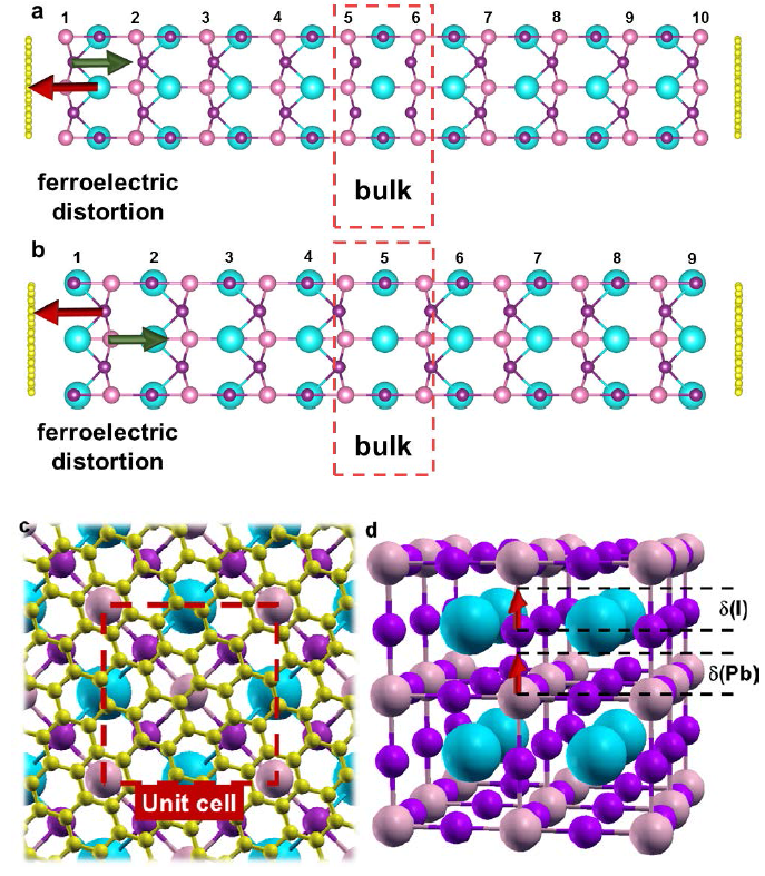
We constructed an interface of graphene/CsPbI3(001)/graphene modeled by a slab of 10(9) layers of PbI2-(CsI-)terminated cubic CsPbI3 with the lattice mismatch 1.93 between two systems (Fig. 1a, 1b and 1c). We confirmed that the surface dipole does not affect both the relaxed geometry and the corresponding electronic structures because the cation and anions (PbI or Cs+I‒) at the termination are oriented parallel to surface. We adopt a symmetric slab sandwiched by graphene at each end to avoid any unphysical artifact. As reported from a previous LDA+D2 calculation of Gr/tetragonal-MAPbI3,Volonakis and Giustino (2015) we observe a ferroelectric distortion driven by an attraction between graphene and cation Pb2+ in the PbI2-termination. A measured distance between PbI2 layer and graphene (Fig. 1a) is 3.21 at the PBE+D3 level and 3.28 at the PBE+TS level of theory which is smaller than LDA+D2 3.45 . As for CsI-termination, a distance between CsI layer and graphene (Fig. 1b) is 3.4 slightly larger than PbI2-terminated surface. Despite the ferroelectric distortion, point symmetry of cubic structure is conserved which is manifested as pure Rashba type splitting in contrast to TiO2/MAPbI3 interface that will be discussed later. Atomic displacements near surface in both cases (Fig. 1a, b) are only significant along [001] (Fig. 1d). However, we observe that the displacement directions of both cases are opposite to each other. For PbI2-termination, the displacements are (Pb) +0.4 and (I) -0.6 , while for MAI-termination, the displacements are (Pb) -0.5 and (I) +0.6 (Fig. 1d). The ferroelectric displacement gradually increases when approaching the interface with its maximum at the very interface. Bulk-like (or inversion symmetric) layers, 5 th and 6 th layer (Fig. 1a and b), is crucial for illustrating a reasonable band structure, unless the band gap closes because of ferroelectricity over the whole structure.Liu et al. (2016) The binding energy (BE) with graphene for PbI¬2-termination is 20.5 /atom, 3.3 times larger than CsI-termination (Table 1).
The electronic band structure of PbI2-(MAI-)terminated Gr/CsPbI3(001)/Gr with PBE+TS+SOC (Fig. 2) reveal some of interesting features. Due to sizable Rashba interactions, in both conduction band (CB) and valence band (VB), surface bands split by momentum and energy . For the bulk cubic (centrosymmetric) CsPbI3 crystal, strong SOC splits the conduction band into one j = 1/2 doublet and one j = 3/2 quartet. Because the valence band is s-like, there is no effective splitting in the highest valence band.Kim et al. (2014b) However, at the Gr/CsPbI3 interface, we note that s-like valence band at M experiences an asymmetric field with respect to the xy plane and its eigenstate is not s = 1/2 but j = 1/2 being mixed with pz state and other states of adjacent layers. This is manifested in the calculated band structure with non-vanishing Rashba splitting of the surface valence band. In CB, the energy splitting between =-1/2 and =1/2 is significant, (PbI2-termination) 280 ; this large barrier would hinder electrons to overcome the barrier from the CB extreme in order to directly recombine with the VB extreme.Yu (2017) Effective Hamiltonian (eq. (1)) should preserve j=1/2 so that the eigenstate of Rashba split bands for both CB and VB are spanned by . Diagonalization of the Hamiltonian gives an entangled spin-orbital texture which resembles the surface state of topological insulator Bi2Se3 (Fig. S1), “spin-momentum locking”.Zhang et al. (2013) Indeed, a recent experiment confirmed an emergence of spin-orbital chiral nature by observing circularly polarized light.Wang et al. (2018) An explicit calculation of direct transition amplitude from conduction band to all valence band states (Fig. S2a) shows that a direct band-to-band transition is largely suppressed due to spin-orbit entanglement and 2D confinement of wavefunction with the ferroelectric distortion,. We also find that Rashba split band promotes the density of states (Fig. 2c).
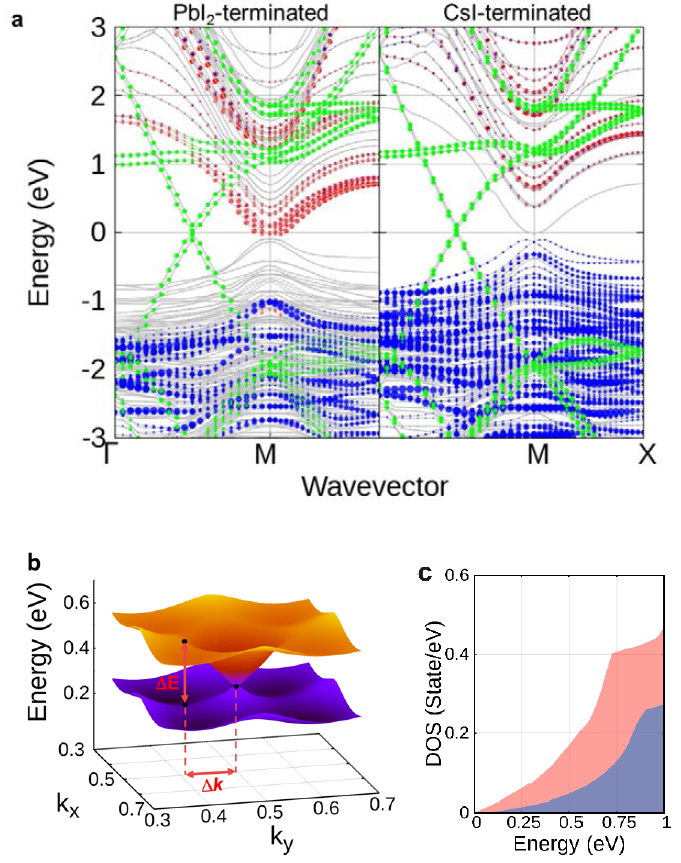
In Gr/CsPbI3(001)/Gr, a surface or gap state shows a rather peculiar structure than usual semi-conductors in which gap states are mainly composed of surface states. For PbI2-termination, while the lowest unoccupied surface state is at the CBM, the highest occupied surface state sits at 1 below the VBM. Interestingly, the maximum of VB is composed of bulk state without Rashba splitting due to its centrosymmetry. The surface state shows the opposite trend in CsI-termination. The highest occupied surface state is the VBM, but the lowest unoccupied surface state is 0.5 above the CBM. The origin of peculiar energy levels of Gr/CsPbI3(001) can be explained by observing the ferroelectric displacement on CsPbI3 surface. It is found that both CsI- and PbI2-terminated CsPbI3(001) experience an intrinsic ferroelectric displacement resembling the relaxed hetero-interface with graphene (Fig. S3). Compared with unrelaxed and relaxed CsPbI3 slabs, significant energy shifts of surface states are observed (Fig. S4). This natural ferroelectric surface distortion would hint the origin of recent observations of Rashba splitting in CsPbBr3 nanocrystal.Isarov et al. (2017) However, the role of graphene differs at each termination. At PbI2 termination, graphene further promotes the ferroelectric distortion and the resulting is enhanced to 0.42(VB) and 1.17(CB) compared with 0.18(VB) and 1.00(CB) of the pristine slab. At CsI termination, graphene suppresses the ferroelectric distortion (Fig. 1b and Fig. S3b) and the RD effect is comparable or even less (Table 1).
The Rashba effect has been shown to exist in bulk MAPbI3: the organic cation MA+ breaks the inversion symmetry and distorts the PbI3 sublattice.Etienne et al. (2016); Kepenekian et al. (2015) However, this effect could be local due to orientational disorder of MA+ cations which significantly reduces the Rashba interaction parameter () at the length scale of 3 . Mosconi et al. (2017); Etienne et al. (2016) Previous work for pristine tetragonal MAPbI3 slab has shown that surface reconstruction could lead to a large RD effect and the effect is more pronounced at PbI2-termination.Mosconi et al. (2016) We calculated the band structure of rutile TiO2/MAPbI3 (001) interface for PbI2-(MAI-) termination (Fig. 3a and 3b) and also the pristine cubic MAPbI3 slab for comparison (Fig. S5). Despite that the bare rutile (001) is not stable, this facet is favored in device configuration.42 (2014) As reported for tetragonal MAPbI3 slab, of CB and VB in the cubic MAPbI3 slab scales by a factor of 2 (Table 1). Also our result is consistent with the previous work showing larger for PbI2-terminated slab evidenced by the distortions of Pb-I bonds along [001] ( 155.5°(PbI2-termination), 170.4 °(MAI-termination)) (Fig. S5).Mosconi et al. (2017)
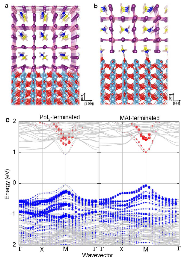
At the PbI2-termination,Mosconi et al. (2016) we observe the bonding between PbO2 ( 2.44 ) and TiI ( 2.9 ).Mosconi et al. (2016) Regarding MAI-terminated interface, our previous work has shown that the orientational freedom of MA+ is significantly curtailed at the TiO2/MAPbI3 interface due to the presence of SSHB between H+ of MA+ and O- of TiO2.Javaid et al. (2017) Indeed, AIMD simulations indicate that the O-H bond at the interface remains intact even at 330 K within cubic phase. Moreover, the optimized MA+ orientation at the interface distorts the PbI3 sublattice by increasing the bond distance between Pb and apical I by 0.15 . Since SSHB considerably reduces the orientational freedom of MA+ at the interface, the Rashba effect at TiO2/MAPbI3 interface should be more robust than the bulk where it is found to be local or semi-local.Leguy et al. (2015) Moreover, the near-pinning effect of MA-orientation at the interface was also confirmed by previous DFT/AIMD simulation studies on stable anatase (101) and (001) interfaces with PSC.Roiati et al. (2014); Long and Prezhdo (2015) Therefore, the robust RD effect by SSHB is expected to be universal over various TiO2/MAPbI3 interface configurations.
In general, the VBM/CBM related states of TiO2 and MAPbI3 lie at high symmetry and M of Brillouin zone (BZ), respectively. The energy splitting is considerably larger for CB (Fig. 3c). This is anticipated as MAPbI3 CB is dominated by heavier Pb states compared with valence states of relatively lighter I atoms. On the other hand, we note that the RD effect has been suppressed at PbI2-terminated interface because of stabilization of the surface via PbO2 and TiI bonding with BE 15.6 /atom. We also observe that a significant distortion along [001] has been quenched ( 172.1°). Therefore, 0.08 (VB) and 0.17 (CB) in TiO2-termination interface is significantly reduced compared to the pristine slab (Table 1). In MAI-terminated interface, SSHB results in enhancing the RD effect for being 0.29 (VBM) and 0.58 (CBM). A momentum (k-space) mismatch is also found between the VBM and CBM as indicated by different Δk for CBM and VBM which suppresses the recombination and increases the carrier lifetime.Motta et al. (2015) As in the case of Gr/CsPbI3, a direct band-to-band recombination of MAPbI3 is significantly quenched being interfaced to TiO2. (Fig. S2b) All the calculated RD interaction parameters are in Table 1.
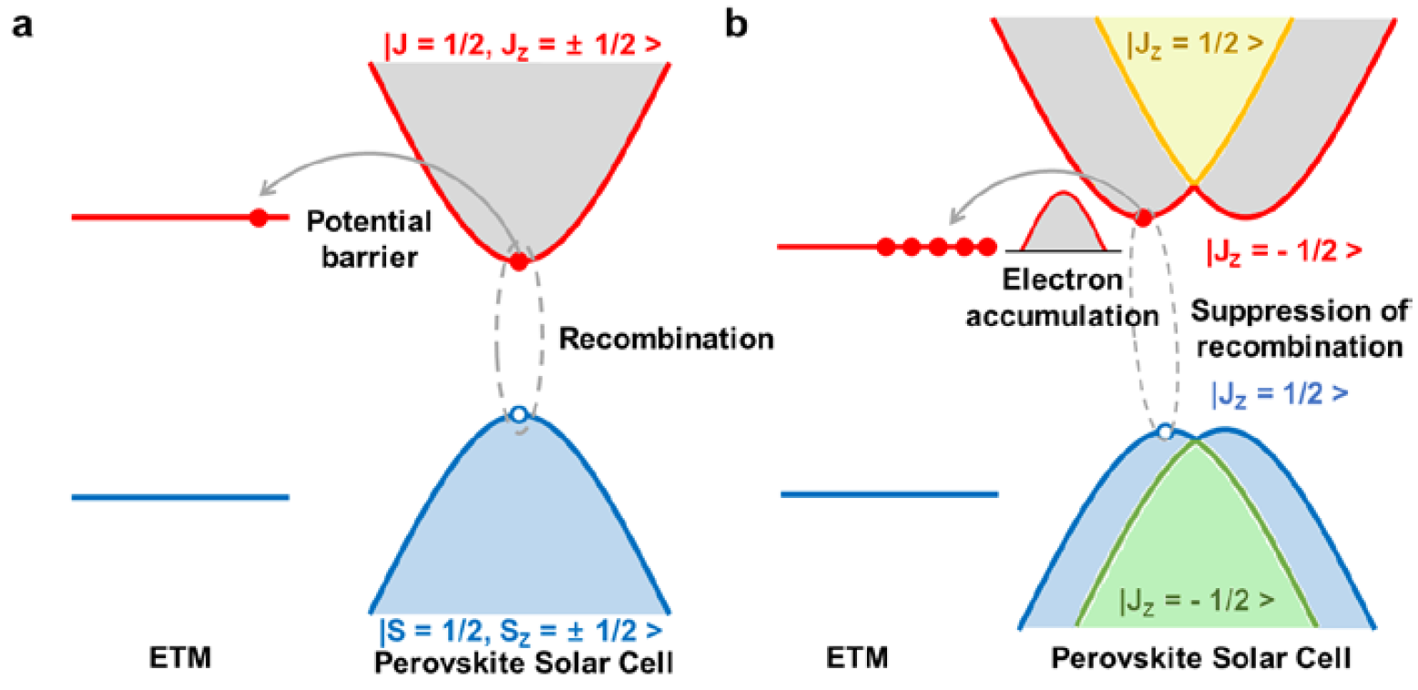
The direct optical measurement and photoemission study have shown that a sizeable electron transfer barrier of 0.4 eV may exist at TiO2/MAPbI3 interface.Xing et al. (2015); Kim et al. (2016b) In the presence of such a large barrier, electron transfer process should be strongly impeded, resulting in accumulation of electrons at interface. In the case that the charge recombination process is favorable, this should result in considerable degradation in device performance. However, the presence of Rashba splitting at the interface (Fig. 3 and Table 1) reduces such recombination process until the potential barrier is overcome by electron accumulation (Fig. 4). Therefore, the presence of Rashba effect at the interface is critical for improving the electron transfer process at the TiO2/MAPbI3 interface.
Apart from 0 K DFT result, to elucidate the impact of thermal degrees of freedom, we average from NVT ensemble based on AIMD simulations around 600 K (for cubic CsPbI3)Hoffman et al. (2016) and 330 K (for cubic MAPbI3).Weller et al. (2015) We choose the most pronounced case, PbI2-termination for Gr/CsPbI3/Gr and MAI-termination TiO2/MAPbI3. Initially we assumed that the RD effect is overestimated in the 0 K DFT. However, the thermal average of RD splitting is found to be comparable to 0 K DFT result (Table 1). Thermal average of (600 K) for PbI2-terminated Gr/CsPbI3 is 0.46(0.15) (VB) and 1.25(0.54) (CB). (330 K) for MAI-terminated TiO2/MAPbI3, where the alignment of MA at the TiO2 interface is kept fixed, is 0.26(0.07) eV·Å (VB) and 0.61(0.15) eV·Å (CB). In particular, the surface I’s configuration does not stray from 0 K configuration even at 330 K because of the enrooted MA (Fig. 3b). Therefore, VB has almost the same as that of 0 K DFT with a negligible standard deviation 0.07.
In summary, we have shown two examples of inorganic/organic perovskite solar cell interfaces: Gr/CsPbI3, a promising interface for efficient carrier transport and TiO2/MAPbI3, a common electron transport layer interface. We report the sizable Rashba interaction (0 K) 1.17 (0.42) and (600 K) 1.25 (0.46) for electron (hole) at PbI2-terminated Gr/CsPbI3. The TiO2/MAPbI3 interface also shows a significant RD interaction (0 K) 0.58 (0.29) and (330 K) 0.61 (0.26) for electron (hole) carriers. The enrooted alignment of MA+ at the TiO2 interface gives rise to a strong and firm RD effect even at high temperatures (¿ 330 K) with small variance. Because of large SOC nature and geometrical complexity of PSCs, its interface with other layers poses rich phenomena. A clever manipulation of such interfaces could accelerate further improvement of the PSC efficiency.
| Interface | BE (meV/atom) | ||
|---|---|---|---|
| CB | VB | ||
| Gr/CsPbI3/Gr (PbI2) | 20.54 | 0.42 | 1.17 |
| Pristine CsPbI3 (PbI2) | - | 0.18 | 1.00 |
| Gr/CsPbI3/Gr (CsI) | 6.23 | 0.59 | 0.50 |
| Pristine CsPbI3 (CsI) | - | 0.53 | 0.54 |
| TiO2/MAPbI3 (PbI2) | 15.64 | 0.08 | 0.17 |
| Pristine MAPbI3 (PbI2) | - | 0.78 | 0.81 |
| TiO2/MAPbI3 (MAI) | 10.33 | 0.29 | 0.58 |
| Pristine MAPbI3 (MAI) | - | 0.18 | 0.30 |
We used Vienna Ab initio Simulation Package (VASP)Tkatchenko and Scheffler (2009) for non-collinear DFT calculations using PBE functional plus Tkatchenko-Scheffler(TS)Grimme et al. (2010)/Grimme DFT-D3Heyd et al. (2003) van der Waals correction with inclusion of spin-orbit coupling by switching off any presumed symmetry. Our previous work has shown that GGA+SOC results are consistent with that of higher level but computationally expensive HSE06Kresse and Furthmuller (1996) +SOC calculations.Liu et al. (2016) For Gr/CsPbI3(001) system, we used kmesh for sampling the Brillouin zone and 500 eV for the energy cutoff. As we checked the convergence of band gap with respect to the thickness of CsPbI3 slab, the convergence has been met from 6 cubic CsPbI3 layers. For TiO2/MAPbI3(001) system, we used kmesh with 520 eV energy cutoff. A supercell consists of 11 rutile TiO2 layers and 3 cubic MAPbI3 layers with (001) orientation for both, where the lattice mismatch using TiO2(001)- is as small as 3 . A vacuum size of 30 is included. We also used Quantum ESPRESSO package v.6.1Giannozzi et al. (2009) with fully relativistic PAW PBE pseudopotential for Pb 6p6s5d, I 5p5s and Cs 6s5p5s at the energy cutoff of 40 Ry. Ab initio MD simulations with time step = 0.5 were performed with total duration of 12 and 30 at 600 K and 330 K for Gr/CsPbI3 and TiO2/MAPbI3, respectively. We sampled NVT configuration using Nosé thermostat and discarded 3 for the initialization.
Acknowledgements.
C.W.M. conceived the idea, performed DFT and AIMD simulations and analyzed the data. S.J. helped in DFT calculation. All discussed and C.W.M., K.S.K. and G.L. wrote the manuscript. This work was supported by National Honor Scientist Program (2010-0020414) and Basic Science Research Program (2015R1C1A1A01055922) of NRF. Computation was supported by KISTI (KSC-2017-S1-0025, KSC-2017-C3-0081).References
- Yang et al. (2017) W. S. Yang, B.-w. Park, E. H. Jung, and N. J. Jeon, Science 1379, 1376 (2017).
- Park et al. (2016) N.-G. Park, M. Grätzel, T. Miyasaka, K. Zhu, and K. Emery, Nature Energy 1, 16152 (2016).
- Juarez-Perez et al. (2014) E. J. Juarez-Perez, R. S. Sanchez, L. Badia, G. Garcia-Belmonte, Y. S. Kang, I. Mora-Sero, and J. Bisquert, Journal of Physical Chemistry Letters 5, 2390 (2014), arXiv:arXiv:1011.1669v3 .
- Fu et al. (2017) J. Fu, Q. Xu, G. Han, B. Wu, C. H. A. Huan, M. L. Leek, and T. C. Sum, Nature Communications 8 (2017), 10.1038/s41467-017-01360-3.
- Yarita et al. (2017a) N. Yarita, H. Tahara, T. Ihara, T. Kawawaki, R. Sato, M. Saruyama, T. Teranishi, and Y. Kanemitsu, Journal of Physical Chemistry Letters 8, 1413 (2017a).
- Myung et al. (2018) C. W. Myung, J. Yun, G. Lee, and K. S. Kim, Advanced Energy Materials 1702898, 1 (2018), arXiv:1711.08938 .
- Wright et al. (2016) A. D. Wright, C. Verdi, R. L. Milot, G. E. Eperon, M. A. Pérez-Osorio, H. J. Snaith, F. Giustino, M. B. Johnston, and L. M. Herz, Nature Communications 7 (2016), 10.1038/ncomms11755.
- Miyata et al. (2017) K. Miyata, D. Meggiolaro, M. T. Trinh, P. P. Joshi, E. Mosconi, S. C. Jones, F. De Angelis, and X.-Y. Zhu, Science Advances 3, e1701217 (2017).
- Frost et al. (2017) J. M. Frost, L. D. Whalley, and A. Walsh, (2017), 10.1021/acsenergylett.7b00862, arXiv:1708.04158 .
- Kim et al. (2014a) J. Kim, S. H. Lee, J. H. Lee, and K. H. Hong, Journal of Physical Chemistry Letters 5, 1312 (2014a).
- Miyata et al. (2015) A. Miyata, A. Mitioglu, P. Plochocka, O. Portugall, J. T. W. Wang, S. D. Stranks, H. J. Snaith, and R. J. Nicholas, Nature Physics 11, 582 (2015), arXiv:1504.07025 .
- Yarita et al. (2017b) N. Yarita, H. Tahara, T. Ihara, T. Kawawaki, R. Sato, M. Saruyama, T. Teranishi, and Y. Kanemitsu, Journal of Physical Chemistry Letters 8, 1413 (2017b).
- Kim et al. (2016a) Y.-H. Kim, H. Cho, and T.-W. Lee, Proceedings of the National Academy of Sciences 113, 11694 (2016a).
- Manchon et al. (2015) A. Manchon, H. C. Koo, J. Nitta, S. M. Frolov, and R. A. Duine, Nature Materials 14, 871 (2015), arXiv:1507.02408 .
- Nitta et al. (1997) J. Nitta, T. Akazaki, H. Takayanagi, and T. Enoki, Physical Review Letters 78, 1335 (1997).
- LaShell et al. (1996) S. LaShell, B. A. McDougall, and E. Jensen, Physical Review Letters 77, 3419 (1996).
- Dedkov et al. (2008) Y. S. Dedkov, M. Fonin, U. Rüdiger, and C. Laubschat, Physical Review Letters 100, 1 (2008), arXiv:0712.3149 .
- Park et al. (2013) Y. H. Park, H.-j. Kim, J. Chang, S. H. Han, J. Eom, H.-j. Choi, and H. Cheol, Appl. Phys. Lett. 252407, 2011 (2013).
- King et al. (2011) P. D. King, R. C. Hatch, M. Bianchi, R. Ovsyannikov, C. Lupulescu, G. Landolt, B. Slomski, J. H. Dil, D. Guan, J. L. Mi, E. D. Rienks, J. Fink, A. Lindblad, S. Svensson, S. Bao, G. Balakrishnan, B. B. Iversen, J. Osterwalder, W. Eberhardt, F. Baumberger, and P. Hofmann, Physical Review Letters 107, 1 (2011), arXiv:arXiv:1103.3220v1 .
- Zhai et al. (2017) Y. Zhai, S. Baniya, C. Zhang, J. Li, P. Haney, C.-X. Sheng, E. Ehrenfreund, and Z. V. Vardeny, Science Advances 3, e1700704 (2017).
- Niesner et al. (2016) D. Niesner, M. Wilhelm, I. Levchuk, A. Osvet, S. Shrestha, M. Batentschuk, C. Brabec, and T. Fauster, Physical Review Letters 117, 1 (2016), arXiv:1606.05867 .
- Isarov et al. (2017) M. Isarov, L. Z. Tan, M. I. Bodnarchuk, M. V. Kovalenko, A. M. Rappe, and E. Lifshitz, Nano Letters 17, 5020 (2017).
- Zheng et al. (2015) F. Zheng, L. Z. Tan, S. Liu, and A. M. Rappe, Nano Letters 15, 7794 (2015), arXiv:1505.04212 .
- Becker et al. (2018) M. A. Becker, R. Vaxenburg, G. Nedelcu, P. C. Sercel, A. Shabaev, M. J. Mehl, J. G. Michopoulos, S. G. Lambrakos, N. Bernstein, J. L. Lyons, T. Stöferle, R. F. Mahrt, M. V. Kovalenko, D. J. Norris, G. Rainò, and A. L. Efros, Nature 553, 189 (2018), arXiv:1707.03071 .
- Mosconi et al. (2017) E. Mosconi, T. Etienne, and F. De Angelis, Journal of Physical Chemistry Letters 8, 2247 (2017).
- Etienne et al. (2016) T. Etienne, E. Mosconi, and F. De Angelis, Journal of Physical Chemistry Letters 7, 1638 (2016).
- Kepenekian et al. (2015) M. Kepenekian, R. Robles, C. Katan, D. Sapori, L. Pedesseau, J. Even, S. Chimiques, C. Uab, and F. Umr, ACS Nano 9, 11557 (2015).
- Rezapour et al. (2017) M. R. Rezapour, C. W. Myung, J. Yun, A. Ghassami, N. Li, S. U. Yu, A. Hajibabaei, Y. Park, and K. S. Kim, ACS Applied Materials and Interfaces 9, 24393 (2017).
- Yan et al. (2015) K. Yan, Z. Wei, J. Li, H. Chen, Y. Yi, X. Zheng, X. Long, Z. Wang, J. Wang, J. Xu, and S. Yang, Small 11, 2269 (2015).
- Ko et al. (2017) K. C. Ko, S. T. Bromley, J. Y. Lee, and F. Illas, The Journal of Physical Chemistry Letters , acs.jpclett.7b02474 (2017).
- Colella et al. (2014) S. Colella, E. Mosconi, G. Pellegrino, A. Alberti, V. L. P. Guerra, S. Masi, A. Listorti, A. Rizzo, G. G. Condorelli, F. De Angelis, and G. Gigli, Journal of Physical Chemistry Letters 5, 3532 (2014).
- Roiati et al. (2014) V. Roiati, E. Mosconi, A. Listorti, S. Colella, G. Gigli, and F. De Angelis, Nano Letters 14, 2168 (2014), arXiv:arXiv:1011.1669v3 .
- Cleland and Kreevoy (1994) W. W. Cleland and M. M. Kreevoy, Science (New York, N.Y.) 264, 1887 (1994).
- Kim et al. (2000) K. S. Kim, K. S. Oh, and J. Y. Lee, Proceedings of the National Academy of Sciences of the United States of America 97, 6373 (2000).
- Volonakis and Giustino (2015) G. Volonakis and F. Giustino, The Journal of Physical Chemistry Letters , 2496 (2015).
- Liu et al. (2016) S. Liu, Y. Kim, L. Z. Tan, and A. M. Rappe, Nano Letters 16, 1663 (2016), arXiv:1508.05625 .
- Kim et al. (2014b) M. Kim, J. Im, A. J. Freeman, J. Ihm, and H. Jin, Proceedings of the National Academy of Sciences 111, 6900 (2014b).
- Yu (2017) Z.-G. Yu, Phys. Chem. Chem. Phys. 19, 14907 (2017).
- Zhang et al. (2013) H. Zhang, C. X. Liu, and S. C. Zhang, Physical Review Letters 111, 2 (2013), arXiv:1211.0762 .
- Wang et al. (2018) R. Wang, S. Hu, X. Yang, X. Yan, H. Li, and C. Sheng, Journal of Materials Chemistry C 6, 2989 (2018).
- Mosconi et al. (2016) E. Mosconi, G. Grancini, C. Roldán-Carmona, P. Gratia, I. Zimmermann, M. K. Nazeeruddin, and F. De Angelis, Chemistry of Materials 28, 3612 (2016).
- 42 (2014) Journal of Materials Chemistry A 2, 9251 (2014).
- Javaid et al. (2017) S. Javaid, C. W. Myung, J.-H. Yun, G. Lee, and K. S. Kim, Journal of Materials Chemistry A 6, 4305 (2017).
- Leguy et al. (2015) A. M. Leguy, J. M. Frost, A. P. McMahon, V. G. Sakai, W. Kochelmann, C. Law, X. Li, F. Foglia, A. Walsh, B. C. O’Regan, J. Nelson, J. T. Cabral, and P. R. Barnes, Nature Communications 6 (2015), 10.1038/ncomms8124, arXiv:1402.4980 .
- Long and Prezhdo (2015) R. Long and O. V. Prezhdo, ACS Nano 9, 11143 (2015).
- Motta et al. (2015) C. Motta, F. El-Mellouhi, S. Kais, N. Tabet, F. Alharbi, and S. Sanvito, Nature communications 6, 7026 (2015), arXiv:1410.8365v2 .
- Xing et al. (2015) G. Xing, B. Wu, S. Chen, J. Chua, N. Yantara, S. Mhaisalkar, N. Mathews, and T. C. Sum, Small 11, 3606 (2015).
- Kim et al. (2016b) Y. K. Kim, B. Jeon, and H. J. Park, Journal of Physical Chemistry C 120, 22460 (2016b).
- Hoffman et al. (2016) J. B. Hoffman, A. L. Schleper, and P. V. Kamat, Journal of the American Chemical Society 138, 8603 (2016).
- Weller et al. (2015) M. T. Weller, O. J. Weber, P. F. Henry, M. D. Pumpo, and T. C. Hansen, Chemical Communications 51, 3 (2015).
- Tkatchenko and Scheffler (2009) A. Tkatchenko and M. Scheffler, Physical Review Letters 102, 6 (2009).
- Grimme et al. (2010) S. Grimme, J. Antony, S. Ehrlich, and H. Krieg, Journal of Chemical Physics 132 (2010), 10.1063/1.3382344, arXiv:0405167 [cond-mat] .
- Heyd et al. (2003) J. Heyd, G. E. Scuseria, and M. Ernzerhof, Journal of Chemical Physics 118, 8207 (2003).
- Kresse and Furthmuller (1996) G. Kresse and J. Furthmuller, Comput. Mater. Sci. 6, 15 (1996).
- Giannozzi et al. (2009) P. Giannozzi et al., J.Phys.: Condens. Matter 21, 395502 (2009).