Resistivity Anomaly in Weyl Semimetal candidate Molybdenum Telluride
Abstract
The Weyl semi-metal candidate MoTe2 is expected to exhibit a range of exotic electronic transport properties. It exhibits a structural phase transition near room temperature that is evident in the thermal hysteresis in resistivity and thermopower (Seebeck coefficient) as well as large spin-orbit interaction. Here, we also document a resistivity anomaly of up to 13% in the temperature window between 25 and 50 K, which is found to be strongly anisotropic. Based on the experimental data in conjunction with density functional theory calculations, we conjecture that the anomaly can be related to the presence of defects in the system. These findings open opportunities for further investigations and understanding of the transport behavior in these newly discovered semi-metallic layered systems.
I Introduction
Transition metal dichalcogenides (TMDC) have received a lot of attention due to a plethora of exciting physical phenomena and their excellent electronic, optical, thermal and mechanical properties Keum et al. (2015); Qi et al. (2016); Mak et al. (2010); Radisavljevic et al. (2010); Splendiani et al. (2010); Ugeda et al. (2014); Mai et al. (2014); Suri and Patel (2017). TMDCs can exist in several different phases displaying a variety of electronic properties including semiconducting, metallic, superconducting, topological insulators and Weyl Fermionic states. Semiconducting TMDCs possess band gaps that change from indirect to direct with the number of layers, facilitating applications such as transistors, photodetectors and electroluminescent devices Wang et al. (2012); Dankert et al. (2014); Dankert and Dash (2017). TMDCs also possess high spin-orbit coupling (SOC), which gives rise to spin polarized surface states in topological insulators Dankert et al. (2015) and Weyl semimetals Fei et al. (2017); Soluyanov et al. (2015). Interestingly, the recently discovered semi-metallic phases of WTe2 and MoTe2 show extremely large non-saturating magnetoresistance Qi et al. (2016); Keum et al. (2015); Ali et al. (2014), signatures of Weyl semimetals Deng et al. (2016); Sun et al. (2015) as well as topological Fermi arcs and surface states Fei et al. (2017), which motivates a further exploration of their fundamental properties.
Here, we investigate the Weyl semi-metal candidate MoTe2 by both electronic transport experiments and density functional theory (DFT) calculations. The basic material properties were investigated by electron, thermal and magneto-transport measurements. We observed the structural phase transition from 1T′ to T in both resistivity and Seebeck coefficient measurements, and significant spin-orbit coupling as evident from weak anti-localization signatures. The samples exhibit a very large and strongly anisotropic resistivity anomaly in the T phase of MoTe2 that occurs between 25 and 50 K.
II Results and Discussions
II.1 Basic characterization
MoTe2 occurs in semiconducting or semi-metallic phases depending on the lattice structure. In the semiconducting phase (2H) each Mo is bonded to six Te atoms in a trigonal prismatic coordination; the three Te sites above the Mo plane are located exactly on-top of the three Te sites below. If one of the Te planes is rotated by 180 degrees one obtains the semimetallic phase (1T), which is, however, unstable toward the 1T′ phase Li et al. (2016). The two semimetallic phases [1T′ and T] that are in fact observed have monoclinic and orthorhombic crystal structures, respectively, and can be thought of as distorted variants of 1T. They differ with respect to the cell angle , which is 93.9∘ for 1T′ and 90∘ for T. Importantly, while 1T′ possesses both time-reversal and inversion symmetries, T does not exhibit inversion symmetry Sankar et al. (2017).
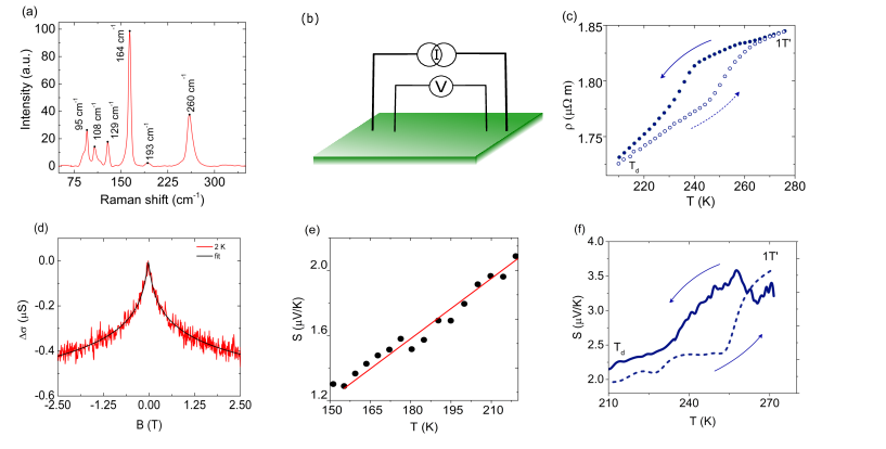
MoTe2 crystals were grown by the chemical vapor transport (CVT) method. Figure Fig. 1(a) shows the Raman spectra where the characteristic peaks corresponding to Ag symmetry were observed at 108 cm-1, 129 cm-1, 164 cm-1, and 260 cm-1. These appearance of these peaks confirms the occurrence of the 1T′ phase at room temperature. Furthermore a peak corresponding to Bg symmetry was observed at 193 cm-1 Oliver et al. (2017); Sankar et al. (2017). We note that although the CVT method to grow TMDCs assures samples of high yield in less time compared to other methods, the approach results in a large number of point defects throughout the crystal. As a result of defects and a high degree of disorder the electronic transport properties of CVT grown samples display some intriguing features Kumar et al. (2017) and were accordingly characterized by means of resistivity, magnetoresistance, and Seebeck measurements. Temperature dependent resistivity measurements were performed on samples of typical dimensions , thickness using the four probe technique [Fig. 1(b)]. The resistivity as a function of temperature exhibits hysteretic behavior around 245 K[Fig. 1(c)], which is attributed to the structural transition from the 1T′ phase at higher temperatures to the T phase at lower temperatures Sankar et al. (2017); Zhang et al. (2016).
Since MoTe2 possesses high spin-orbit coupling, weak anti-localization (WAL) measurements were carried out as well. In this case, application of an out-of-plane magnetic field breaks the time-reversal symmetry, and reduces the conductivity correction () as shown in Fig. 1(d). The conductivity reduction is a signature of WAL and can be fitted by the Hikami-Larkin-Nagaoka (HLN) model Hikami et al. (1980), which yields a phase coherence length of .
The Seebeck coefficient increases linearly with temperature between 150 and 220 K [Fig. 1(e)] as expected for a metallic phase Snyder and Toberer (2008); Tian et al. (2014); Ashcroft and Mermin (1976). The thermal hysteresis apparent in the resistivity measurements is also observed in the same temperature range in the Seebeck coefficient [Fig. 1(f)]. As before the hysteresis is caused by the structural phase transition from the T to the 1T′ phase, and is also observed for other samples [see Fig. S2 (b) of the Supplementary Information SupplementaryInformation ].
II.2 Resistivity anomaly
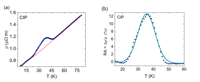
Having established that the basic characteristics of our samples in the temperature window between approximately 150 K to room temperature match those expected for the known semi-metallic phases of MoTe2, we can now focus on the low-temperature behavior. Here, the temperature dependent resistivity obtained at a pressure of reveals a resistivity anomaly (RA) that sets in around a particular temperature of T36 K [Fig. 2]. The resistivity anomaly is defined as
| RA (%) | (1) |
In the present case, we find a RA of up to 13 %, which is best described by a Gaussian fit. Such anomalies in TMDCs have been found to be sensitive to various factors including, e.g., impurities, doping, and pressure Zocco et al. (2015); Ritschel et al. (2013). Our measurements have been repeated on different samples and reproduced consistently (see Figs. S3 (a,b) of the Supplementary Information SupplementaryInformation ). To confirm that the signature is purely from the sample, a control experiment was also performed on a Cu wire in similar experimental conditions, which showed normal metallic behavior [Fig. S3 (c)]. Given the growth method, which as discussed above tends to be associated with a relatively high defect density and the WAL analysis, We tentatively attribute these anomalies to defects incorporated during synthesis.
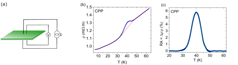
In MoTe2, the intra-layer bonding is strong and covalent, whereas the inter-layer bonding is due to weak van-der-Waals forces, leading to strong anisotropy in many properties. Measurements were therefore also performed in current-perpendicular-to-plane (CPP) configuration, where the current flows perpendicular to the sample planes [Fig. 3(a)]. The thermal hysteresis (corresponding to the 1T′-T structural transition close to room temperature) observed in CPP mode was centered at 254 K. The degree of anisotropy estimated from the comparison of the resistivity measured in CIP and CPP modes is 103. In the CPP measurement configuration is centered at 40 K [Fig. 3(b)], which is close to the temperature of 36 K obtained in CIP geometry. The RA obtained in CPP mode is, however, 6 % and thus about half of that observed in CIP mode (13.1%) [Fig. 3(c)]. The reduction of the resistivity anomaly in CPP mode compared to CIP mode may be attributed to the high degree of structural anisotropy. In particular, since the weak van-der-Waals gap inter-layers bonding is associated with soft phonon modes, one can expect the electron-phonon coupling strength to be very anisotropic.
In order to gain further understanding of the experimental results, density functional theory (DFT) calculations were performed using the project augmented wave (PAW) method Blöchl (1994); Kresse and Joubert (1999) as implemented in the Vienna ab-initio simulation package Kresse and Furthmüller (1996). Structural relaxation and total energy calculations were carried out using the vdW-DF-cx exchange-correlation functional Dion et al. (2004); Berland and Hyldgaard (2014), which has been previously shown to provide an excellent description of the lattice structure of semiconducting TMDCs with van-der-Waals bonding Lindroth and Erhart (2016). While spin-orbit coupling (SOC) is important given the large mass of Te, the spin-polarized version of vdW-DF-cx has not yet been verified for such calculations yet. The electronic structure including SOC effects was therefore computed using the PBE fucntional Perdew et al. (1996) on the vdW-DF-cx relaxed structures. The structures were relaxed until the maximum force in the system was less than 5 meV/Å. The plane wave cutoff energy was set to 400 eV and the Brillouin zone was sampled suing a Monkhorst-Pack grid.
While the calculated in-plane lattice parameters are in very good agreement with experiment, the out-of-plane lattice parameter in the metallic phases of MoTe2 is underestimated by compared to experimental data Sankar et al. (2017). In this context, it is interesting to note that in the case of WSe2 a similar difference for the out-of-plane lattice constant was observed between conventionally and turbostratically grown crystals of the 2H phase Nguyen et al. (2010); Erhart et al. (2015), which could be attributed to the larger density of stacking faults in the latter material. Since the vdW-DF-cx method otherwise reproduces the results for the ideal crystal structures of TMDCs very well, the discrepancy could be another telltale sign of the rather higher defect density in the present samples that was already alluded to above. A comprehensive comparison of the calculated lattice parameters can be found in the Supplementary Material.
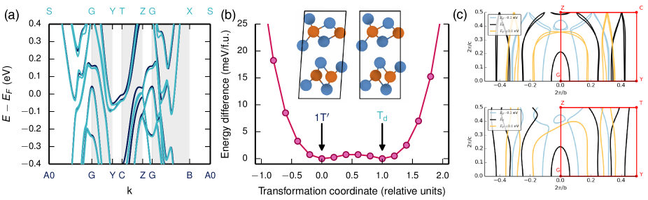
The electronic band structures of bulk 1T′ and T MoTe2 show a multi-valley structure with many pockets and band inversions. Generally, they are very similar [Fig. 4 (a)] with noticeable differences only along the Y-C (Y-T) and C-Z (T-Z) paths in the Brillouin zone of T (1T′). According to our calculations, the ideal 1T′ and T structures are energetically practically degenerate and separated by a very small transition barrier of about 1 meV/f.u. [Fig. 4 (b)]. This extremely soft landscape suggests that these phases can be very sensitive to thermal perturbations and defects. The most striking difference in the electronic band structure is the pinching of the energy bands close to the Fermi energy at the zone boundary near in the T phase [Fig. 4 (c)], a feature that is absent in the case of 1T′. Qualitatively, this means that the orbits in T are closed, whereas the obits are open in 1T′. We note, however, that the precise location of (and number of) the Weyl points in the T phase is known to be very sensitive to the structural parameters Tamai et al. (2016), and even small changes in the lattice parameter (due to thermal expansion or defects) might change the Fermi surface considerably and thus affect electrical transport in the material.
III Conclusions
To summarize, we have carried out transport measurements on semi-metallic MoTe2 in various temperature ranges. MoTe2 showed semi-metallic properties with high spin-orbit coupling, structural phase transitions from Td to 1T′ near to room temperature in the temperature dependent resistivity (in both CIP and CPP measurement geometries) and Seebeck coefficient measurements. We observed a pronounced resistivity anomaly up to 13% at low temperature with a strong anisotropy of 103 (three orders of magnitude) between the CIP and CPP measurement configuration. The resistivity anomaly can be attributed to point defects created during the synthesis of MoTe2 by chemical vapor transport process. The DFT calculations performed suggest that the resistivity anomaly is not present in the pristine crystal, which further supports the attribution to defects. This work forges a path for further investigation of metastable state leading to reorganization in the electron density and its relation to chiral symmetry breaking in various Weyl semi-metal candidates.
IV Acknowledgements
DS thanks Department of Science and Technology (DST), Government of India for a PhD fellowship through the DST-INSPIRE program (No. DST/INSPIRE Fellowship/2013/742). RSP thanks the DST, Government of India for financial support through the Nanomission program (No. SR/NM/NS-1002/2010 (G)) and SERB grant (No. EMR/2016/003318). SPD thanks financial supports from the European Union Graphene Flagship (No. 604391), a FlagEra project (VR No. 2015-06813), and the Swedish Research Council (No. 2016-03658). CL, SKS, and PE acknowledge support from the Knut and Alice Wallenberg Foundation.
Corresponding Authors:
R. S. Patel: rsp@goa.bits-pilani.ac.in; Saroj P. Dash: saroj.dash@chalmers.se; Paul Erhart: erhart@chalmers.se
References
- Keum et al. (2015) D. H. Keum, S. Cho, J. H. Kim, D.-H. Choe, H.-J. Sung, M. Kan, H. Kang, J.-Y. Hwang, S. W. Kim, H. Yang, K. J. Chang, and Y. H. Lee, Nat. Phys. 11, 482 (2015).
- Qi et al. (2016) Y. Qi, P. G. Naumov, M. N. Ali, C. R. Rajamathi, W. Schnelle, O. Barkalov, M. Hanfland, S.-C. Wu, C. Shekhar, Y. Sun, V. Sub, M. Schmidt, U. Schwarz, E. Pippel, P. Werner, R. Hillebrand, T. Förster, E. Kampert, S. Parkin, R. J. Cava, C. Felser, B. Yan, and S. A. Medvedev, Nat. Phys. 7, 11038 (2016).
- Mak et al. (2010) K. F. Mak, C. Lee, J. Hone, J. Shan, and T. F. Heinz, Phys. Rev. Lett. 105, 136805 (2010).
- Radisavljevic et al. (2010) B. Radisavljevic, A. Radenovic, J. Brivio, V. Giacometti, and A. Kis, Nat. Nanotechnol. 6, 147 (2010).
- Splendiani et al. (2010) A. Splendiani, L. Sun, Y. Zhang, T. Li, J. Kim, C.-Y. Chim, G. Galli, and F. Wang, Nano Lett. 10, 1271 (2010).
- Ugeda et al. (2014) M. M. Ugeda, A. J. Bradley, S.-F. Shi, F. H. da Jornada, Y. Zhang, D. Y. Qiu, W. Ruan, S.-K. Mo, Z. Hussain, Z.-X. Shen, F. Wang, S. G. Louie, and M. F. Crommie, Nat. Mat. 13, 1091– (2014).
- Mai et al. (2014) C. Mai, A. Barrette, Y. Yu, Y. G. Semenov, K. W. Kim, L. Cao, and K. Gundogdu, Nano Lett. 14, 202 (2014).
- Suri and Patel (2017) D. Suri and R. S. Patel, Appl. Phys. Lett. 110, 233108 (2017).
- Wang et al. (2012) Q. H. Wang, K. Kalantar-zadeh, A. Kis, J. N. Coleman, and M. S. Strano, Nat. Nanotechnol. 7, 699 (2012).
- Dankert et al. (2014) A. Dankert, L. Langouche, M. V. Kamalakar, and S. P. Dash, ACS Nano 8, 476 (2014).
- Dankert and Dash (2017) A. Dankert and S. P. Dash, Nat. Commun. 8, 16093 (2017).
- Dankert et al. (2015) A. Dankert, J. Geurs, M. V. Kamalakar, S. Charpentier, and S. P. Dash, Nano Lett. 15, 7976 (2015).
- Fei et al. (2017) Z. Fei, T. Palomaki, S. Wu, W. Zhao, X. Cai, B. Sun, P. Nguyen, J. Finney, X. Xu, and D. H. Cobden, Nat. Phys. 13, 677 (2017).
- Soluyanov et al. (2015) A. A. Soluyanov, D. Gresch, Z. Wang, Q. Wu, M. Troyer, X. Dai, and B. A. Bernevig, Nature 527, 495 (2015).
- Ali et al. (2014) M. N. Ali, J. Xiong, S. Flynn, J. Tao, Q. D. Gibson, L. M. Schoop, T. Liang, N. Haldolaarachchige, N. P. O. Max Hirschberger, and R. J. Cava, Nature 514, 205–208 (2014).
- Deng et al. (2016) K. Deng, G. Wan, P. Deng, K. Zhang, S. Ding, E. Wang, M. Yan, H. Huang, H. Zhang, Z. Xu, J. Denlinger, A. Fedorov, H. Yang, W. Duan, H. Yao, Y. Wu, y. S. Fan, H. Zhang, X. Chen, and S. Zhou, Nat. Phys. 12, 1105–1110 (2016).
- Sun et al. (2015) Y. Sun, S.-C. Wu, M. N. Ali, C. Felser, and B. Yan, Phys. Rev. B 92, 161107 (2015).
- Li et al. (2016) Y. Li, K.-a. N. Duerloo, K. Wauson, and E. J. Reed, Nat. Commun. 7, 10671 (2016).
- Sankar et al. (2017) R. Sankar, G. N. Rao, I. P. Muthuselvam, C. Butler, N. Kumar, G. S. Murugan, C. Shekhar, T.-R. Chang, C.-Y. Wen, C.-W. Chen, W.-L. Lee, M. Lin, H.-T. Jeng, C. Felser, and F. C. Chou, Chem. Mater. 29, 699 (2017).
- Oliver et al. (2017) S. M. Oliver, R. Beams, S. Krylyuk, A. K. Singh, A. Bruma, J. Joshi, I. R. Stone, S. J. Stranick, A. V. Davydov, and P. M. Vora, 2D Mater. 4, 045008 (2017).
- Kumar et al. (2017) N. Kumar, C. Shekhar, M. Wang, Y. Chen, H. Borrmann, and C. Felser, Phys. Rev. B 95, 155128 (2017).
- Zhang et al. (2016) K. Zhang, C. Bao, Q. Gu, X. Ren, H. Zhang, K. Deng, Y. Wu, and Y. Li, Nature Communications 7, 13552 (2016).
- Hikami et al. (1980) S. Hikami, A. Larkin, and Y. Nagaoka, Prog. Theor. Phys. 63, 707 (1980).
- Snyder and Toberer (2008) G. J. Snyder and E. S. Toberer, Nat. Mater. 7, 105 (2008).
- Tian et al. (2014) Z. Tian, S. Lee, and G. Chen, ArXiv e-prints (2014), arXiv:1401.0749 [cond-mat.mtrl-sci] .
- Ashcroft and Mermin (1976) N. W. Ashcroft and N. D. Mermin, “Solid state physics,” (CENAGE Learning, 1976) p. 256.
- (27) SupplementaryInformation, .
- Zocco et al. (2015) D. A. Zocco, J. J. Hamlin, K. Grube, J.-H. Chu, H.-H. Kuo, I. R. Fisher, and M. B. Maple, Phys. Rev. B 91, 205114 (2015).
- Ritschel et al. (2013) T. Ritschel, J. Trinckauf, G. Garbarino, M. Hanfland, M. v. Zimmermann, H. Berger, B. Büchner, and J. Geck, Phys. Rev. B 87, 125135 (2013).
- Blöchl (1994) P. E. Blöchl, Phys. Rev. B 50, 17953 (1994).
- Kresse and Joubert (1999) G. Kresse and D. Joubert, Phys. Rev. B 59, 1758 (1999).
- Kresse and Furthmüller (1996) G. Kresse and J. Furthmüller, Comp. Mater. Sci. 6, 15 (1996).
- Dion et al. (2004) M. Dion, H. Rydberg, E. Schröder, D. C. Langreth, and B. I. Lundqvist, Phys. Rev. Lett. 92, 246401 (2004).
- Berland and Hyldgaard (2014) K. Berland and P. Hyldgaard, Phys. Rev. B 89, 035412 (2014).
- Lindroth and Erhart (2016) D. O. Lindroth and P. Erhart, Phys. Rev. B 94, 115205 (2016).
- Perdew et al. (1996) J. P. Perdew, K. Burke, and M. Ernzerhof, Phys. Rev. Lett. 77, 3865 (1996).
- Nguyen et al. (2010) N. T. Nguyen, P. A. Berseth, Q. Lin, C. Chiritescu, D. G. Cahill, A. Mavrokefalos, L. Shi, P. Zschack, M. D. Anderson, I. M. Anderson, and D. C. Johnson, Chem. Mater. 22, 2750 (2010).
- Erhart et al. (2015) P. Erhart, P. Hyldgaard, and D. O. Lindroth, Chemistry of Materials 27, 5511 (2015).
- Tamai et al. (2016) A. Tamai, Q. S. Wu, I. Cucchi, F. Y. Bruno, S. Riccò, T. K. Kim, M. Hoesch, C. Barreteau, E. Giannini, C. Besnard, A. A. Soluyanov, and F. Baumberger, Phys. Rev. X 6, 031021 (2016).