Quantum phase transition in few-layer NbSe2 probed through quantized conductance fluctuations
Abstract
We present the first observation of dynamically modulated quantum phase transition (QPT) between two distinct charge density wave (CDW) phases in 2-dimensional 2H-NbSe2. There is recent spectroscopic evidence for the presence of these two quantum phases, but its evidence in bulk measurements remained elusive. We studied suspended, ultra-thin 2H-NbSe2 devices fabricated on piezoelectric substrates - with tunable flakes thickness, disorder level and strain. We find a surprising evolution of the conductance fluctuation spectra across the CDW temperature: the conductance fluctuates between two precise values, separated by a quantum of conductance. These quantized fluctuations disappear for disordered and on-substrate devices. With the help of mean-field calculations, these observations can be explained as to arise from dynamical phase transition between the two CDW states. To affirm this idea, we vary the lateral strain across the device via piezoelectric medium and map out the phase diagram near the quantum critical point (QCP). The results resolve a long-standing mystery of the anomalously large spectroscopic gap in NbSe2.
Despite intensive research over several decades, charge density waves (CDW) continue to remain at the forefront of modern condensed matter physics Grüner (1988); Miller et al. (2012); Monceau (2012). CDW in quasi-one dimension is understood to arise from Peierls mechanism - an inherent instability of a coupled electron-phonon system which creates a gap in the single-particle excitation spectrum leading to the emergence of a collective mode formed of electron-hole pairs Peierls (1991).
In higher dimensions this electron-phonon interaction induced renormalization of the lattice wave vectors is often not enough to give rise to CDW Matsuno et al. (2001); Yan et al. (2017); Johannes and Mazin (2008); Yan et al. (2017); Arguello et al. (2015); Valla et al. (2004); Suderow et al. (2005); Castro Neto (2001); Cercellier et al. (2007); Castellan et al. (2013); Ishioka et al. (2010). One of the best known examples is 2H-NbSe2, where the mechanism of CDW is still widely debated Ugeda et al. (2016); Weber et al. (2013); Borisenko et al. (2009); Johannes et al. (2006); Weber et al. (2011); Flicker and Van Wezel (2015). It has been suggested that the origin may lie in the strong momentum and orbital dependence of the electron-phonon coupling Johannes et al. (2006); Weber et al. (2011). A natural consequence of this is the sensitivity of the CDW order to lattice perturbations. This has recently been verified by Scanning Tunneling Microscopy (STM) measurements, which find the existence of 1Q striped quantum phase competing with the standard 3Q phase in locally strained regions Soumyanarayanan et al. (2013). The tri-directional 3Q phase respects the three-fold lattice symmetry and has a periodicity , where is the reciprocal lattice vector. The 1Q is a linear phase with a periodicity Soumyanarayanan et al. (2013). Calculations indicate that, for , the system is very close to a quantum critical point separating these two phases and any small perturbation, like local strain, can induce a quantum phase transition (QPT) between these two Flicker and Van Wezel (2015); Flicker and van Wezel (2015, 2016). There are however, no direct experimental evidences of this QPT.
We probe for the possible existence of QPT in ultra-thin, suspended 2H-NbSe2 devices through time dependent conductance fluctuation spectroscopy Ghosh et al. (2004). We find that, for devices where the strain is dynamic, the electrical conductance fluctuates between two precise values separated by a quantum of conductance, with a well defined time scale. These fluctuations can be quenched either by damping out the strain fluctuations or by introducing lattice disorder into the system. We can control the transition between the two distinct quantum states by modulating the strain in devices fabricated on piezoelectric substrates. Through detailed calculations and analysis, we show that our observations are consistent with strain induced dynamic fluctuations between 3Q and 1Q quantum phases in 2H-NbSe2. We also establish that the energy scale of 35 meV, often seen in spectroscopy studies in 2H-NbSe2, is associated with the energy barrier separating the two CDW phases.
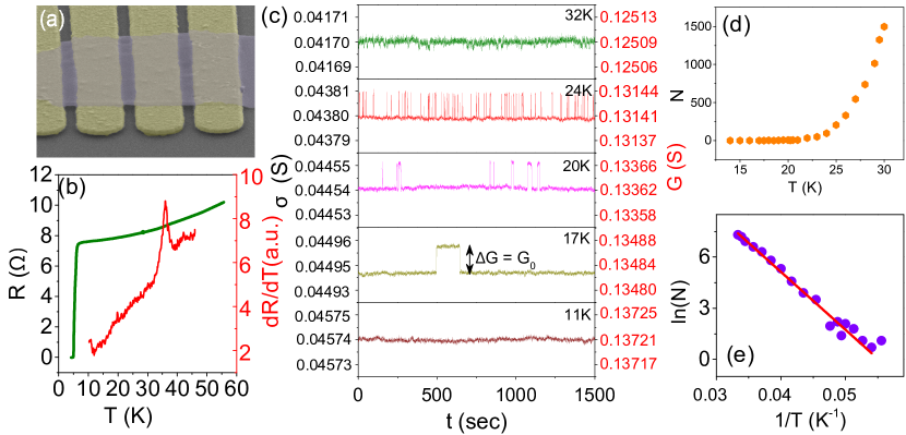
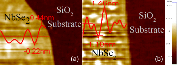
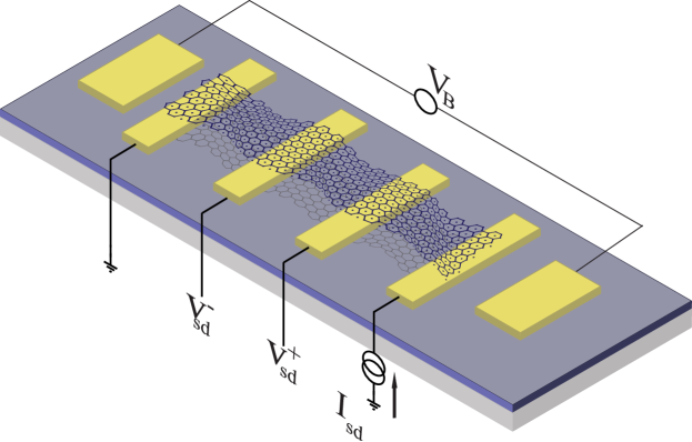
We study two classes of devices. The first class, which we call ‘on-substrate’, is prepared on SiO2/Si++ substrates by mechanical exfoliation from bulk 2H-NbSe2 followed by standard electron beam lithography Ganguli et al. (2016). The second class of devices is suspended - few-layer 2H-NbSe2 flakes were mechanically exfoliated from bulk single crystals on silicone elastomer polydimethylsiloxane (PDMS) and transferred onto Au electrodes pre-fabricated on either SiO2/Si++ or BaTiO3/SrTiO3 substrates. The aspect ratios (width/length ratio) of the samples were close to an integer, ranging from two to six. To study the effect of disorder, both these classes of devices are fabricated from multiple bulk 2H-NbSe2 crystals having a range of superconducting Tc and residual resistivity ratios ) Ganguli et al. (2016). Devices are also fabricated from bulk 2H-NbSe2 doped with cobalt to introduce disorder in a controlled manner. The devices range in thickness from bilayer to about 50 nm, as obtained both from optical contrast and AFM measurements [Supplementary Information]. A SEM image of a typical suspended device is shown in figure 1(a).
Figure 1(b) shows the evolution of the resistance, with temperature, of a suspended tri-layer device S1. The onset of CDW at K is indicated by a peak in the dR/dT plot. The high value of the residual resistivity ratio, 8.5 and the relatively high superconducting , 6 K indicate the defect free nature of the device. The time series of conductance fluctuations at different is plotted in figure 1(c). For very close to , the time series consists of random fluctuations about the average value, arising from the generic noise in the device. Below 30 K, we find the appearance of Random telegraphic noise (RTN) with the conductance fluctuating between two well defined levels separated by the quantum of conductance, . The RTN persists right down to about 12 K below which superconducting fluctuations become dominant. The measurements are repeated on clean, suspended devices of different flake thicknesses. It was seen that with increasing thickness, the magnitude of the conductance jumps increased, remaining in all cases close to an integer multiple of [Supplementary Materials Fig. S5]. Figure 1(d) shows a plot of the total number of switches over a period of 30 minutes at different temperatures. The switching statistics could be well described by an Arrhenius function [Fig. 1(e)]. The magnitude of the activation energy was found to be lie in the range meV in all such suspended, clean devices.
To probe in detail the statistics of the RTN, we performed low frequency resistance fluctuation spectroscopy at different temperature using a digital signal processing (DSP) based ac technique [Supplementary Information]. At each temperature the resistance fluctuations were recorded for 30 minutes. The resultant time-series of resistance fluctuations were digitally decimated and anti-aliased filtered. The power spectral density (PSD) of resistance fluctuations, was calculated from this filtered time series using the method of Welch periodogram Ghosh et al. (2004). The was subsequently integrated over the bandwidth of measurement to obtain the relative variance of resistance fluctuations: =.
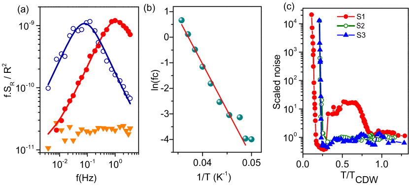
Figure 2(a) shows the measured PSD at a few representative temperatures. We find that the PSD over the temperature window 12 KT30 K deviate significantly from nature, this range coinciding with that over which RTN was seen [Fig. 1(c)]. The PSD of an RTN is a Lorentzian of corner frequency where is the time scale of the resistance switches between the two levels. Motivated by this, we analyzed the PSD data using the relation:
| (1) |
The first term in Eqn. 1 represents the generic noise in the device, while the second term quantifies the contribution from a Lorentzian Fagerquist et al. (1989). Constants A and B measure the relative strengths of the two terms and are derived from the fits to the experimental data [Fig. 2(a)]. We find to be thermally activated, [figure 2(b)]. The value of the energy barrier is found to be 3 meV, which matches very well with that obtained from an analysis of the RTN jump statistics.
The relative variance of resistance fluctuations , normalized by its value at 60 K, is plotted in Fig. 2(c). The noise shows a broad peak over the temperature range where RTN are present. We have verified that the additional contribution to the noise in this temperature range arises from the Lorentzian component in the PSD. We find that over the temperature range where RTN are absent, the distribution of resistance fluctuations is Gaussian, as is expected for uncorrelated fluctuations. With decreasing , shoots up because of the onset of superconducting fluctuations. This has been seen before in many different superconducting systems and will not be discussed further in this letter Koushik et al. (2013); Daptary et al. (2016); Shi et al. (2016).
Turning now to the origin of these RTNs, we note that these can possibly arise, in CDW systems which have a single-particle energy gap at the Fermi level (e.g. NbSe3 and TaS3) Bloom et al. (1994a); Marley et al. (1994); Bloom et al. (1994b), due to the switching of the ground state of the system between pinned and sliding states. In some of these systems sharp noise peaks were observed even at values of electric fields lower than the threshold field for slippage of the CDW Zaïtsev-Zotov and Pokrovskiï (1989).Our results differ from what was observed in these systems in two important aspects: (1) our measurements were performed under electric fields of magnitude few V/m which were at least two orders of magnitude smaller than the electric fields applied to observe RTN in these systems Zaïtsev-Zotov and Pokrovskiï (1989); Bloom et al. (1994a); Marley et al. (1994); Bloom et al. (1994b), and (2) unlike in NbSe3 and TaS3, the observed RTN in 2H-NbSe2 were independent of electric field Zaïtsev-Zotov and Pokrovskiï (1989). However, unlike NbSe3 and TaS3, the CDW in 2H-NbSe2 does not slide. This is consistent with our observation that the RTN in 2H-NbSe2 were independent of electric field. This suggests that RTN in 2H-NbSe2 must have an origin distinct from those seen in gapped CDW systems like NbSe3 and TaS3.
There is a due concern that the observed RTN may arise due to the interplay of superconducting fluctuations above and CDW order. Measurements performed under perpendicular magnetic fields much higher than of bulk 2H-NbSe2 do not have any effect on either the frequency or the amplitude of these two level fluctuations, ruling out this interpretation [Supplementary information]. We also considered the possibility that the RTN can arise due to the quantization of the number of density waves along the perpendicular direction, as seen in some systems Kummamuru and Soh (2008); Jaramillo et al. (2007). We ruled this out by noting that in 2H-NbSe2 the weak inter-layer van der waals interaction precludes the formation of any long range density waves perpendicular to the planes. This is supported by spectroscopic studies.
The most compelling explanation of the RTN we observe in 2H-NbSe2 is phase fluctuations between 1Q and 3Q phases. Earlier calculations Flicker and van Wezel (2015), supported by the STM measurements Soumyanarayanan et al. (2013), demonstrated that the crossover between 3Q and a 1Q CDW phases at a given temperature can be induced by a strain as small as 0.1%. Experiments show that suspended 2H-NbSe2 devices in contact with Au pads experience an average strain of about 0.1% at low temperatures Sengupta et al. (2010) which is sufficient to drive the system close to the boundary separating these two quantum phases Flicker and van Wezel (2015). In such a suspended mesoscopic device, at a finite temperature, the strain dynamically fluctuates due to thermally enhanced mechanical vibrations. This fluctuating strain can lead to a dynamical phase transition from 3Q to 1Q and vice versa in 2H-NbSe2 at a fixed temperature. This would cause the conductance of the system to fluctuate between two well defined values if the conductivity of the two phases are different. We validate this conjecture through detailed Density-functional theory (DFT) based band structure calculations of the conductance in the two distinct quantum phases of 2H-NbSe2.
We calculate the DC conductivity in both the 3Q and 1Q CDW phases using a two-band model, relevant for this compound Rossnagel et al. (2001). The non-interacting dispersions are directly deduced from the DFT calculations [Supplementary Information]. 111 The wavevector of the CDW state is known to be , where are the three reciprocal lattice vectors, and in the 3Q phase. In the 1Q phase, only one of the values remain active along the CDW propagation direction (we take ). The CDW order parameters are introduced within the mean-field approximation:
| (2) | |||||
Here the band index , and the nesting index takes 3 values in the 3Q phase and 1 value in the 1Q phase. is the annihilation operator for the electron in the -band at momentum . The mean-field CDW gap is defined between the two bands. We obtain the quasiparticle energies by exact diagonalization of the Hamiltonian in (2), and there are four, and eight quasiparticle states in the 1Q and 3Q phases, respectively.
The conductivity of the two phases primarily depends on the CDW gap values , which are related to the CDW potential by , with . The interaction arises from the electron-phonon coupling (Flicker and van Wezel, 2015) and is directly related to strain, and therefore it becomes directional dependent. A CDW phase arises along a direction when the corresponding strain induced potential exceeds the critical potential , where is the bandwidth. Since the present system reside in the vicinity of the critical point, , and the phase diagram is very sensitive to strain. In the 3Q phase, all three , while in 1Q phase, only , and the rest are .
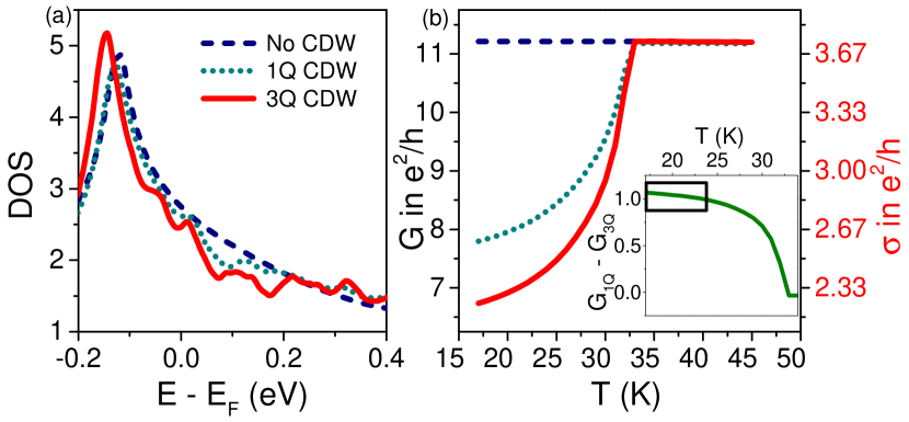
In the mean-field state, we find a substantial suppression of the density of state (DOS) at in the 3Q phase, with a gap which is calculated to be 35 meV [Fig. 3(a)]. However, in the 1Q phase, the spectral weight loss at is significantly less. These results are consistent with the STM data Soumyanarayanan et al. (2013). Therefore, we anticipate that the conductivity in the 3Q phase will be lower than that in the 1Q phase.
We first calculate the conductivity using the standard Kubo formula. We then obtain the conductance G by normalizing the value of with the dimensions of the present device ((width/length)). We assume band independent gap values. For the ratio of , we find that the difference in conductance between the two CDW phases, , as seen experimentally. We also notice that over the temperature range 17K-24K, changes very little as the self-consistent gap remains essentially unchanged over this narrow temperature window [Fig. 3(b)]. This result is consistent with our experimental observations. We do not have a microscopic understanding of why this quantity should be an integral multiple of . This may require the inclusion of topological terms in the calculation which is beyond the scope of the present work.
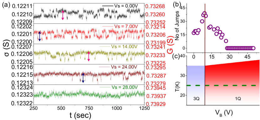
If dynamical phase fluctuations between the two CDW phases is indeed responsible for the observed RTN, it should be possible to modulate the frequency of the conductance jumps by driving the system controllably between the two competing CDW phases. To test this hypothesis, suspended devices of few layer 2H-NbSe2 are fabricated on piezoelectric BaTiO3/SrTiO3 (BTO) substrates. In this device, the strain across the device can be modulated by varying the voltage across the substrate. Fig. 4(a) shows the evolution of the conductance fluctuations with changing obtained for one such device at 25 K. At very low values of (strain), the frequency of the conductance jumps is low and the system is seen to spend statistically similar amounts of time in both the high and low conductance states. With increasing (and consequently increasing strain across the device), the frequency of the conductance jumps initially increases and then decreases rapidly. However, the magnitude of the conductance jumps throughout this process remained quantized in units of . Eventually, the conductance jumps vanishes as the system stabilized in the higher conduction state [Fig. 4(b)]. We note that in different sweep cycles in the RTN are not exactly reproducible. It is difficult at this stage to comment on whether this is due to inherent hysteresis in the piezoelectric response of BTO or if it indicates non-reversibility of the properties of NbSe2.
These results can be understood as follows: with increasing strain via , the system approaches the phase boundary separating the 3Q and 1Q phases, leading to an increased probability of switching between the two states. Eventually, the system crosses the phase boundary and consequently, the switching frequency starts decreasing and finally vanishes as the system settles into the 1Q state. These measurements establish conclusively that, consistent with theoretical calculations, strain can drive the system to the higher conducting 1Q phase from lower conducting 3Q phase.
As seen from STM measurements on substrated devices, local random strain due to lattice imperfections causes the system to spatially phase separate into an inhomogeneous mixture of 3Q and 1Q phases Soumyanarayanan et al. (2013). This local phase separation can not cause the measured conductance, which is a macroscopic global averaged property, to fluctuate dynamically between two well defined conductance levels separated by the quantum of conductance. To validate this conjecture, measurements were performed on 2H-NbSe2 devices of various thicknesses prepared on SiO2/Si++ substrates [Supplementary Information]. Although we observed clear CDW transition in this set of devices from resistivity measurements, no signature of RTN was seen in any of them. The conductance fluctuations in these devices, at all temperatures , consisted only of generic fluctuations arising from defect dynamics. The magnitude of noise remained constant over the temperature range before showing the sharp rise near superconducting transition [Fig. 2(c)].
To test the effect of disorder, measurements were performed on suspended devices exfoliated from bulk 2H-NbSe2 crystals having low bulk Tc and low residual resistivity ratio and from bulk 2H-NbSe2 crystals doped with 0.1% Co. Atomic Force microscopy measurements showed that the rms surface roughness of the low Tc flakes was about 3 times higher than that of the high Tc flakes [Supplementary Information]. Although we observed dR/dT peak at 35 K in these devices indicating the presence of CDW, we did not observe RTN in any of them. The noise in these devices was similar to what was seen for substrated devices indicating the suppression of RTN due to disorder in the system [Fig. 2(c)]. The absence of RTN in all the control experiments involving substrated, Co-doped and disordered suspended 2H-NbSe2 devices, as well as the insensitivity of the conductance fluctuations in clean suspended devices to high magnetic fields reinforces our interpretation of the origin of the observed RTN in clean suspended devices as lattice fluctuation mediated.
To conclude, in this letter we demonstrate controlled, strain induced phase transition between the 1Q and 3Q CDW phases in suspended 2D 2H-NbSe2. With this, we resolve a long standing question of finite temperature dynamic phase transition between two quantum phases of the CDW system. We show the energy scale of 35meV, seen repeatedly in spectroscopic measurements Borisenko et al. (2009); Soumyanarayanan et al. (2013), to be the barrier corresponding to 1Q-3Q phase transition. Our work establishes conductance fluctuation spectroscopy as a technique to probe phase co-existence and phase transitions in nanoscale systems and can thus be a step forward in the understanding of competing quantum phases in strongly correlated systems.
A.B. acknowledges financial support from Nanomission, DST, Govt. of India project SR/NM/NS-35/2012; SERB, DST, Govt. of India and Indo-French Centre for the Promotion of Advanced Recearch (CEFIPRA). H.K.K. thanks CSIR, MHRD, Govt. of India for financial support. TD acknowledgesthe financial support from the DST, India under the Start Up Research Grant (Young Scientist) [SERB No: YSS/2015/001286]. We acknowledge discussions with A. V. Mallik, B. F. Gao, D. Nordlund, A. N. Pasupathy and Diptiman Sen.
Supplementary Information
S1 Effect of magnetic field on the observed RTN:
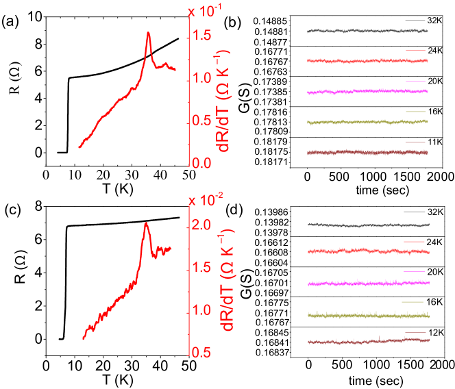
In many low-dimensional superconductors, superconducting fluctuations can persist at temperatures much higher than the mean field transition temperature . In the case of our cleanest bulk samples, the measured was . Thus, there might be a concern that the two-level conductance fluctuations observed by us in the clean suspended 2H-NbSe2 flakes at 15 K and above might have some contributions from superconducting phase/amplitude fluctuations. To rule out this possibility, we have studied the effect of magnetic field (with much larger than the critical field ) on the observed RTN. Fig. S1 shows plots of conductance fluctuation measured at 24 K at zero field and in the presence of an 8 T perpendicular field, the data are statistically identical showing that magnetic field had no discernible effect on the two-level conductance fluctuations.
S2 Resistance fluctuation spectroscopy:
To probe resistance fluctuation and its statistics, we used a standard 4-probe digital signal processing (DSP) based ac noise measurement technique Ghosh et al. (2004). This technique allows us to simultaneously measure the background noise as well as sample noise. The device was biased by a constant ac current source, typical currents used during the measurement were 10 A. A low-noise pre-amplifier (SR552) was used to couple the voltage across the device to dual channel digital lock-in-amplifier (LIA). The bias frequency of the LIA (228 Hz) was chosen to lie in the eye of the noise figure of the pre-amplifier to reduce the contribution of amplifier noise. The output of the LIA was digitized by a high speed 16 bit analog-to-digital conversion card and stored in computer. The complete data set for each run, containing data points, was decimated and digitally filtered to eliminate the 50 Hz line frequency component. This filtered time series was then used to calculate the power spectral density (PSD) of voltage fluctuation SV over specified frequency window using the method of Welch Periodogram. The lower frequency limit mHz and the upper frequency limit Hz were limited by the ratio of the sample noise to background noise. The PSD of voltage fluctuation was converted to the PSD of resistance fluctuation by the relation where is rms value of constant current used to bias the device. The measurement set up has been calibrated by thermal noise measurements on standard resistors to measure spectral density down to . The measured thermal background noise on the 2H-NbSe2 devices were found to be bias independent and frequency independent; and the PSD matched the value of 4, as expected from Johnson-Nyquist noise. The PSD of resistance fluctuation was subsequently integrated over the bandwidth of measurement to obtain the relative variance of resistance fluctuations:
S3 Absence of RTN in on-substrate and disordered 2H-NbSe2 devices:
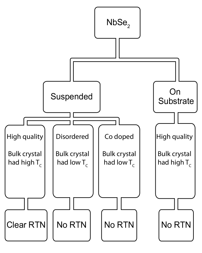
To conclusively establish that the RTN seen by us in 2H-NbSe2 is present only in suspended clean devices, we fabricated on-substrate devices from the same high quality bulk 2H-NbSe2 from which the suspended devices showing RTN were exfoliated. In all our substrated device, we observed CDW transition with similar TCDW 35 K but did not find signatures of RTN at any temperature [fig. S3]. Similarly, suspended devices fabricated from bulk 2H-NbSe2 crystals having low superconducting , despite undergoing a CDW transition at 35 K, did not show any RTN as shown in S3[d]. These control experiments confirm that the two-level conductance fluctuations seen by us are a property of clean suspended 2H-NbSe2 devices. We have performed AFM measurements to map the topography of the flakes and their thicknesses. It was observed that flakes exfoliated from bulk crystal of lower TC had a much higher surface roughness ( 3-4 times) than those from high quality bulk crystals - the AFM topography images are shown in fig. S2. The observation of RTN in all the different classes of samples measured is summarised in fig. S4. This flowchart shows that RTN is observed only in suspended devices made from disorder free flakes.
In Ref. Soumyanarayanan et al. (2013) the two phases are found to coexist due to non-uniform local strains because of underlying defects – these devices were all on substrate. Since the thermodynamic phase of the system is well defined in the temperature-phase plane, for uniform strain the whole sample will undergo the transformation simultaneously in which case there is no phase co-existence. Thus, we believe that the coexistence between the two phases happens only in the case of non-uniform strain. It should be noted that for non-uniform strain, fractional steps in conductance could be expected. We explain below why we do not see them in our measurements.
As seen from the data presented in Soumyanarayanan et al. (2013), in on-substrate devices the domains are of the order of ten nm and more importantly, are static in time. This nanoscale phase separation is detectable in STM tunneling spectroscopic measurements which is a local probe. Our transport measurements, on the other hand, were time-dependent and performed between electrical probes separated by hundreds of nanometers. That is why we do not observe any conductance jumps from the static nanoscale phase separation seen in the on-substrate devices of the type studied in Ref. Soumyanarayanan et al. (2013).
We note that for Co-doped samples one can expect fractional jumps. Unfortunately, we do not observe any RTN in the case of suspended Co-doped 2H-NbSe2 devices. We believe that this can be due to disorder inhibiting the formation of long range order in the system. It is also possible that Co doping might modify the phonon dispersion spectrum and suppress the formation of one of the two CDW phases. Further experimental and theoretical work is required to settle this issue.
S4 Quantization of conductance fluctuation:
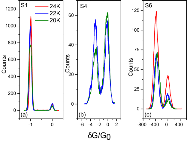
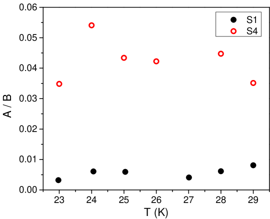
We have measured different suspended devices with different thickness and observed that the two level conductance fluctuation is always present with the conductance jump of integer multiple of . We have found that for thicker samples the jump is larger than thinner ones. In fig. S5 the distribution function of conductance fluctuation is plotted. The conductance jump is 1 and 3 for the two thin samples, S1 and S4 and is large 370 for the thick sample S6. It can be seen from the data that the quantization is seen most clearly in the thinnest flakes. This is because, for thicker devices, the ratio of the magnitude of noise to the amplitude of RTN jumps is much larger than that in thin flakes. As discussed in the manuscript, this ratio is parametrized by the quantity (see discussion following Eqn. 1 in the main text). For example, for the sample S4 this ratio was ten times higher than that in sample S1 (Fig. S7). This higher 1/f noise cause the peaks to broaden for thicker samples.
S5 Number of layers participating in RTN
An important question is whether all the layers in the flake contribute to the observed RTN. In case of suspended devices where RTN is seen with strain, we can envisage two possible scenarios which are as follows. First probable case is that the bottom layer gets strained and the top layers slip on this layer to relax the strain. This will entail an energy cost, due to non-conformity between the layers. We estimate this energy cost for relative displacement between two layers of 2H-NbSe2 to be about eV/unit cell Levita et al. (2014); Nagapriya et al. (2008); Shmeliov et al. (2014) [See Fig. S8]. An alternate scenario is where all the layers get strained equally. We estimate the elastic energy cost in this process, for small strains of the magnitude applied by us (0.1%), to be about eV/unit cell Sengupta et al. (2010). It thus appears that it is energetically favourable for all the layers to strain together by the same amount. The reality of course could lie somewhere in between these two extremes - especially for very thick flakes where it is highly plausible that the strain relaxes beyond the first few layers.
S6 Details of DFT calculations
Electronic structure of bilayer 2H-NbSe2 was calculated by using density functional theory (DFT) with the generalized gradient approximation (GGA) in the parametrization of Perdew, Burke and Ernzerhof Perdew et al. (1996) as implemented in the Vienna ab-initio simulation package Kresse and Furthmüller (1996). Projected augmented-wave (PAW) Kresse and Joubert (1999) pseudopotentials are used to describe core electrons.The electronic wavefunction is expanded using plane waves up to a cut-off energy of 600 eV. Brillouin zone sampling is done by using a 12 12 1 Monkhorst-Pack k-grid for the primitive unit-cell’s calculations. The conjugate gradient method is used to obtain relaxed geometries. Both atomic positions and cell parameters are allowed to relax, until the forces on each atom are less than 0.01 eV/Angstrom.
Force constants were calculated for a 331 supercell within the framework density functional perturbation theory Gonze (1995) using the VASP code. Subsequently, phonon dispersions were calculated using phonopy package[Togo et al. (2008)].
We calculate the conductivity using the standard Kubo formula.
| (3) |
where is the Fermi-distribution function, is the band velocity. , and have the usual meanings. is the spectral function which is obtained from the imaginary part of the Green’s function obtained from Eq. 2. We averaged the conductivity over the entire Basel plane as . The temperature dependence of the conductivity comes from the Fermi function , as well as from the -dependence of the gap, and its behavior is dominated by the latter function.

Control: key (0) Control: author (8) initials jnrlst Control: editor formatted (1) identically to author Control: production of article title (-1) disabled Control: page (0) single Control: year (1) truncated Control: production of eprint (0) enabled
References
- Grüner (1988) G. Grüner, Rev. Mod. Phys. 60, 1129 (1988).
- Miller et al. (2012) J. H. Miller, A. I. Wijesinghe, Z. Tang, and A. M. Guloy, Phys. Rev. Lett. 108, 036404 (2012).
- Monceau (2012) P. Monceau, Advances in Physics 61, 325 (2012), http://dx.doi.org/10.1080/00018732.2012.719674 .
- Peierls (1991) R. E. Peierls, More surprises in theoretical physics, Vol. 19 (Princeton University Press, 1991).
- Matsuno et al. (2001) J. Matsuno, A. Fujimori, L. F. Mattheiss, R. Endoh, and S. Nagata, Phys. Rev. B 64, 115116 (2001).
- Yan et al. (2017) S. Yan, D. Iaia, E. Morosan, E. Fradkin, P. Abbamonte, and V. Madhavan, Phys. Rev. Lett. 118, 106405 (2017).
- Johannes and Mazin (2008) M. D. Johannes and I. I. Mazin, Phys. Rev. B 77, 165135 (2008).
- Arguello et al. (2015) C. J. Arguello, E. P. Rosenthal, E. F. Andrade, W. Jin, P. C. Yeh, N. Zaki, S. Jia, R. J. Cava, R. M. Fernandes, A. J. Millis, T. Valla, R. M. Osgood, and A. N. Pasupathy, Phys. Rev. Lett. 114, 037001 (2015).
- Valla et al. (2004) T. Valla, A. V. Fedorov, P. D. Johnson, P.-A. Glans, C. McGuinness, K. E. Smith, E. Y. Andrei, and H. Berger, Phys. Rev. Lett. 92, 086401 (2004).
- Suderow et al. (2005) H. Suderow, V. G. Tissen, J. P. Brison, J. L. Martínez, and S. Vieira, Phys. Rev. Lett. 95, 117006 (2005).
- Castro Neto (2001) A. H. Castro Neto, Phys. Rev. Lett. 86, 4382 (2001).
- Cercellier et al. (2007) H. Cercellier, C. Monney, F. Clerc, C. Battaglia, L. Despont, M. G. Garnier, H. Beck, P. Aebi, L. Patthey, H. Berger, and L. Forró, Phys. Rev. Lett. 99, 146403 (2007).
- Castellan et al. (2013) J.-P. Castellan, S. Rosenkranz, R. Osborn, Q. Li, K. E. Gray, X. Luo, U. Welp, G. Karapetrov, J. P. C. Ruff, and J. van Wezel, Phys. Rev. Lett. 110, 196404 (2013).
- Ishioka et al. (2010) J. Ishioka, Y. H. Liu, K. Shimatake, T. Kurosawa, K. Ichimura, Y. Toda, M. Oda, and S. Tanda, Phys. Rev. Lett. 105, 176401 (2010).
- Ugeda et al. (2016) M. M. Ugeda, A. J. Bradley, Y. Zhang, S. Onishi, Y. Chen, W. Ruan, C. Ojeda-Aristizabal, H. Ryu, M. T. Edmonds, H.-Z. Tsai, et al., Nature Physics 12, 92 (2016).
- Weber et al. (2013) F. Weber, R. Hott, R. Heid, K.-P. Bohnen, S. Rosenkranz, J.-P. Castellan, R. Osborn, A. H. Said, B. M. Leu, and D. Reznik, Phys. Rev. B 87, 245111 (2013).
- Borisenko et al. (2009) S. Borisenko, A. Kordyuk, V. Zabolotnyy, D. Inosov, D. Evtushinsky, B. Büchner, A. Yaresko, A. Varykhalov, R. Follath, W. Eberhardt, et al., Physical review letters 102, 166402 (2009).
- Johannes et al. (2006) M. Johannes, I. Mazin, and C. Howells, Physical Review B 73, 205102 (2006).
- Weber et al. (2011) F. Weber, S. Rosenkranz, J.-P. Castellan, R. Osborn, R. Hott, R. Heid, K.-P. Bohnen, T. Egami, A. Said, and D. Reznik, Phys. Rev. lett. 107, 107403 (2011).
- Flicker and Van Wezel (2015) F. Flicker and J. Van Wezel, Nature communications 6 (2015).
- Soumyanarayanan et al. (2013) A. Soumyanarayanan, M. M. Yee, Y. He, J. van Wezel, D. J. Rahn, K. Rossnagel, E. Hudson, M. R. Norman, and J. E. Hoffman, Proceedings of the National Academy of Sciences 110, 1623 (2013).
- Flicker and van Wezel (2015) F. Flicker and J. van Wezel, Physical Review B 92, 201103 (2015).
- Flicker and van Wezel (2016) F. Flicker and J. van Wezel, Physical Review B 94, 235135 (2016).
- Ghosh et al. (2004) A. Ghosh, S. Kar, A. Bid, and A. Raychaudhuri, arXiv preprint cond-mat/0402130 (2004).
- Ganguli et al. (2016) S. C. Ganguli, H. Singh, I. Roy, V. Bagwe, D. Bala, A. Thamizhavel, and P. Raychaudhuri, Physical Review B 93, 144503 (2016).
- Fagerquist et al. (1989) R. Fagerquist, R. D. Kirby, and E. A. Pearlstein, Physical Review B 39, 5139 (1989).
- Koushik et al. (2013) R. Koushik, S. Kumar, K. R. Amin, M. Mondal, J. Jesudasan, A. Bid, P. Raychaudhuri, and A. Ghosh, Physical review letters 111, 197001 (2013).
- Daptary et al. (2016) G. N. Daptary, S. Kumar, P. Kumar, A. Dogra, N. Mohanta, A. Taraphder, and A. Bid, Phys. Rev. B 94, 085104 (2016).
- Shi et al. (2016) Z. Shi, X. Shi, and D. Popović, Physical Review B 94, 134503 (2016).
- Bloom et al. (1994a) I. Bloom, A. Marley, and M. Weissman, Physical Review B 50, 5081 (1994a).
- Marley et al. (1994) A. Marley, I. Bloom, and M. Weissman, Physical Review B 49, 16156 (1994).
- Bloom et al. (1994b) I. Bloom, A. Marley, and M. Weissman, Physical Review B 50, 12218 (1994b).
- Zaïtsev-Zotov and Pokrovskiï (1989) S. V. Zaïtsev-Zotov and V. Y. Pokrovskiï, JETP Lett 49 (1989).
- Kummamuru and Soh (2008) R. K. Kummamuru and Y.-A. Soh, Nature 452, 859 (2008).
- Jaramillo et al. (2007) R. Jaramillo, T. F. Rosenbaum, E. D. Isaacs, O. G. Shpyrko, P. G. Evans, G. Aeppli, and Z. Cai, Phys. Rev. Lett. 98, 117206 (2007).
- Sengupta et al. (2010) S. Sengupta, H. S. Solanki, V. Singh, S. Dhara, and M. M. Deshmukh, Phys. Rev. B 82, 155432 (2010).
- Rossnagel et al. (2001) K. Rossnagel, O. Seifarth, L. Kipp, M. Skibowski, D. Voß, P. Krüger, A. Mazur, and J. Pollmann, Phys. Rev. B 64, 235119 (2001).
- Note (1) The wavevector of the CDW state is known to be , where are the three reciprocal lattice vectors, and in the 3Q phase. In the 1Q phase, only one of the values remain active along the CDW propagation direction (we take ).
- Ghosh et al. (2004) A. Ghosh, S. Kar, A. Bid, and A. Raychaudhuri, arXiv preprint cond-mat/0402130 (2004).
- Soumyanarayanan et al. (2013) A. Soumyanarayanan, M. M. Yee, Y. He, J. van Wezel, D. J. Rahn, K. Rossnagel, E. Hudson, M. R. Norman, and J. E. Hoffman, Proceedings of the National Academy of Sciences 110, 1623 (2013).
- Levita et al. (2014) G. Levita, A. Cavaleiro, E. Molinari, T. Polcar, and M. Righi, The Journal of Physical Chemistry C 118, 13809 (2014).
- Nagapriya et al. (2008) K. Nagapriya, O. Goldbart, I. Kaplan-Ashiri, G. Seifert, R. Tenne, and E. Joselevich, Physical review letters 101, 195501 (2008).
- Shmeliov et al. (2014) A. Shmeliov, M. Shannon, P. Wang, J. S. Kim, E. Okunishi, P. D. Nellist, K. Dolui, S. Sanvito, and V. Nicolosi, ACS nano 8, 3690 (2014).
- Sengupta et al. (2010) S. Sengupta, H. S. Solanki, V. Singh, S. Dhara, and M. M. Deshmukh, Phys. Rev. B 82, 155432 (2010).
- Perdew et al. (1996) J. P. Perdew, K. Burke, and M. Ernzerhof, Physical review letters 77, 3865 (1996).
- Kresse and Furthmüller (1996) G. Kresse and J. Furthmüller, Physical review B 54, 11169 (1996).
- Kresse and Joubert (1999) G. Kresse and D. Joubert, Physical Review B 59, 1758 (1999).
- Gonze (1995) X. Gonze, Physical Review A 52, 1086 (1995).
- Togo et al. (2008) A. Togo, F. Oba, and I. Tanaka, Physical Review B 78, 134106 (2008).