Center for Transport and Devices of Emergent Materials, Technische Universität Dresden, 01062 Dresden, Germany \alsoaffiliationTechnische Universität Dresden, Institute of Materials Science, 01062 Dresden, Germany \alsoaffiliationTechnische Universität Dresden, Institute of Materials Science, 01062 Dresden, Germany \alsoaffiliationCenter for Transport and Devices of Emergent Materials, Technische Universität Dresden, 01062 Dresden, Germany \alsoaffiliationCenter for Transport and Devices of Emergent Materials, Technische Universität Dresden, 01062 Dresden, Germany
Spin-Hall-Active Platinum Thin Films Grown Via Atomic Layer Deposition
Abstract
We study the magnetoresistance of yttrium iron garnet/Pt heterostructures in which the Pt layer was grown via atomic layer deposition (ALD). Magnetotransport experiments in three orthogonal rotation planes reveal the hallmark features of spin Hall magnetoresistance. We estimate the spin transport parameters by comparing the magnitude of the magnetoresistance in samples with different Pt thicknesses. We compare the spin Hall angle and the spin diffusion length of the ALD Pt layers to the values reported for high-quality sputter-deposited Pt films. The spin diffusion length of agrees well with platinum thin films reported in the literature, whereas the spin Hall magnetoresistance is approximately a factor of 20 smaller compared to that of our sputter-deposited films. Our results demonstrate that ALD allows fabricating spin-Hall-active Pt films of suitable quality for use in spin transport structures. This work provides the basis to establish conformal ALD coatings for arbitrary surface geometries with spin-Hall-active metals and could lead to 3D spintronic devices in the future.
Atomic layer deposition (ALD) is a powerful process that allows 3D conformal coatings.1 ALD has been extensively used for the deposition and conformal coating of thin oxide insulator films onto nanopatterned templates or flat substrates. Increasingly more metals can also be deposited using ALD, and deposition processes have already been developed for several metals.1, 2
In particular, the ALD of Pt has been investigated by several groups. Different precursor chemistries based on trimethyl(methylcyclopentadienyl)platinum, \chPt(CpMe)Me3,3, 4 or platinum acetylacetonate, \chPt(acac)2, 5 have been reported, with the former generally resulting in films with higher conductivity.
Pt with its strong spin-orbit coupling is one of the key materials for modern spintronics, allowing the efficient conversion of charge currents to spin currents and vice versa, i.e., leading to a large spin Hall effect.6, 7 Thus, the ALD of Pt could open the door for 3D metallic nanostructures with spintronic functionality, for instance structures dependent on high aspect ratios, such as racetrack memory.8, 9
Additionally, interesting phenomena related to spin transport in non-planar geometries (e.g. coated nanowires) were recently proposed.10
In particular, the propagation length of spin/magnon currents in such curved geometries should crucially depend on the spin current’s polarization direction.10, 11, 12
To determine by electrical transport whether spin generation and detection are also feasible in such structures, spin Hall magnetoresistance (SMR) can be used. SMR is a powerful tool for determining the spin transport parameters in ferromagnetic insulator (FMI)/non-ferromagnetic metal (NM) heterostructures.13, 7, 14 In particular, the magnitude of the SMR effect as a function of the NM thickness allows inferring the spin Hall angle and the spin diffusion length of the normal metal and the FMI/NM interface quality quantified by the spin mixing conductance .13
Here, we show that Pt films grown via ALD are indeed spin Hall active. Specifically, we observe an SMR with magnitude in heterostructures consisting of an yttrium iron garnet (\chY3Fe5O12, YIG) thin film covered by a Pt layer grown by ALD. This is clear evidence for spin-Hall-driven spin current transport across the YIG/Pt interface.
Thus, our study establishes the ALD deposition of Pt, a prototypical material that is widely used as a detector/injector for spin currents. This provides an important contribution toward the realization of spin transport experiments in non-planar/non-trivial geometries and might lead to spintronic applications in 3D geometries in the future.
We started from commercially available, thick YIG films grown via liquid phase epitaxy on \chGd3Ga5O12 substrates. Then, we used the established cleaning and pre-preparation procedure to prepare our ex situ YIG/Pt samples.15, 16
The YIG films were cleaned using piranha etching solution (3\chH2SO4:1\chH2O2) for one minute to remove organic residue from the surface.16 Subsequently, the samples were submerged in distilled or de-ionized water and loaded into the ALD chamber while still covered with water. The two different sets of equipment and parameters that were used for growing the Pt films are denoted as series A and series B.
The growth of series A was performed in a commercially available GemStar XT-R thermal bench-top ALD system from Arradiance. \chMe(CpPt)Me3 was used as the Pt precursor with pure oxygen (\chO2) as the oxidizer. The chamber temperature was set to , and the organic precursor was preheated to in order to increase the evaporation rate. The pulse and exposure times of the \chMe(CpPt)Me3 were set to and , respectively, followed by a pumping time for the removal of any residual precursor and the reactants. For pulsing the Pt precursor, the so-called boost mode was used, in which \chAr was inserted into the \chMe(CpPt)Me3 precursor bottle to increase the amount of precursor inserted into the chamber. For the second half-cycle, \chO2 was pulsed for with subsequent exposure and pumping times of and , respectively. For the samples grown within series A, 100 and 280 cycles were performed, resulting in thicknesses of nm and nm, respectively.
The platinum films for series B were grown in a Gemstar-6 ALD reactor, which is also commercially available from Arradiance. The same organic precursor was used, but the oxidizer was replaced with ozone (\chO3) due to its higher reactivity. The ozone was provided by a BMT 803N ozone generator. The organic precursor was heated to , while the reactor chamber was set to . The pulse and exposure times of the Pt precursor were set to and , respectively. The pulse and exposure steps were performed two times to ensure a saturation of the sample surface with the organic precursor. Afterward, the precursor residue and the reactants were purged from the chamber in a pump interval. Subsequently, \chO3 was pulsed for , followed by an exposure time of and a pump time of . Herewith, 160 (240) cycles result in a Pt thickness of nm (nm). A summary of the growth parameters of both series A and B is presented in Tab. 1.
| series A | series B | |
| Chamber temperature Tch [∘C] | 250 | 220 |
| Precursor temperature TPt [∘C] | 68 | 50 |
| Pt: tp/texp/tpump [s] | 0.05*/20/60 | 0.5/30†/90 |
| O2|O3: tp/texp/tpump [s] | 0.02/4/60 | 0.5/30/90 |
Additionally, a reference sample was prepared with a sputtered Pt film, where the YIG film was additionally annealed in the ultra-high-vacuum of the deposition chamber at after the piranha etch to further improve the interfacial quality and to mimic the temperature of the ALD process.
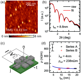
To investigate the surface topology, atomic force microscopy (AFM) was performed to extract the rms roughness of our films. An AFM measurement of a sample with yields a roughness of that is consistent with comparable films shown in the literature.7 Furthermore, the exact thickness of the films was determined by X-ray reflectometry (XRR) measurements and subsequent fitting of the obtained curves. An exemplary set of data and the respective fit are shown in Fig. 1(b).
After finishing the structural characterization, Hall bars were patterned into the Pt layers (cf. Fig. 1(a)) using optical lithography and subsequent dry etching with \chAr ions. The Hall bars have a length of and a width of .
To establish electrical contact to our setup, the samples were glued to a chip carrier and contacted via wedge bonding with aluminum wire. To quantify the magnetoresistive response, the samples were mounted in a magnet setup with a cylindrical Halbach array.17 It features a constant magnetic flux density of perpendicular to the array’s cylindrical axis.
To obtain the magnetoresistance, we drive a current of along the Hall bar with a Keithley 2450 sourcemeter while simultaneously recording the voltage drop with a Keithley 2182 nanovoltmeter. To further improve the measurement sensitivity and to remove spurious contributions, we employ a current reversal technique.18
The resistivity of the samples as a function of the platinum thickness is shown in Fig. 1(d). As expected for platinum and all other metals, a sharp increase in the resistivity toward low thicknesses is observed, which is consistent with previous reports.19, 20 We use Eq. (1) to fit the data and extract the mean free path in our platinum layers assuming that we are in the diffusive limit.21 The fit yields a bulk resistivity of and an electron mean free path of when using the roughness of as determined by AFM.
| (1) |
The extracted mean free electron path and the bulk resistivity agree well with values reported for evaporated platinum thin films.20
To determine the angular dependence of the magnetoresistance, the Halbach array and thus the magnetic field are rotated around the cylindrical axis. Using three different sample inserts, we define the (mutually orthogonal) rotation planes of the magnetic field. For in-plane rotations (ip), the magnetic field is rotated in the film plane around the surface normal . For the other two rotation planes, with a finite component of the magnetic field out of the film plane (oop), the magnetic field is either rotated around the direction of the current flow (oopj) or the transverse direction (oopt). The three rotation planes are shown as insets in Fig. 2(a-c).
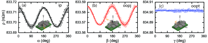
The obtained magnetoresistance for a YIG/Pt (ALD) film with is shown in Fig. 2. The resistivity of Pt is strongly temperature dependent; therefore, a linear drift was subtracted from the data to compensate for the slow drifts of the sample temperature. Since the SMR only depends on the projection of the magnetization onto the direction,7, 13 i.e. , , we expect to observe a modulation for the ip and oopj configurations and no modulation for the oopt rotation. This is fully corroborated by our experimental observations. In other words, Fig. 2 shows the characteristic fingerprint of SMR in our YIG/Pt heterostructures also for ALD-grown Pt.
The magnitude of the SMR for the sample shown in Fig. 2 is . Comparing these values to our reference sample with a sputtered Pt film (), the SMR amplitude is reduced by a factor of 20 and is smaller by a factor of 40 when compared to the best YIG/Pt heterostructures with similar Pt thicknesses.7 This result leads to two possible conclusions: either the interface of the heterostructure is not ideal or the quality of the Pt film is decreased by using ALD. However, the electrical characterization of our films contradicts the latter. Consequently, we assume that contributions such as organic contaminants at the interface or the cleaning procedure should be further optimized to take ALD-specific requirements into account.
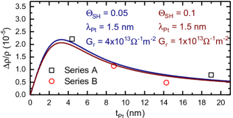
To further analyze the relevant transport parameters in our heterostructures, we investigate the thickness dependence of the SMR (c.f. Fig. 3). As expected for SMR, the magnitude of the MR decreases for increasing thickness.13
| (2) |
Using two different sets of parameters adapted from the study by Althammer et al.7 together with the bulk resistivity and Eq. (2), we can reproduce the trend of the thickness dependence (c.f. dark red and dark blue curves in Fig. 3). However, to also obtain a good fit of the magnitude of our data, we have to reduce the spin mixing conductance by approximately a factor of 10. The two sets of parameters are summarized in Fig. 3. Additionally, from the two parameter sets, it is clear that the spin Hall angle and the spin mixing conductance are closely related and that their influence cannot be trivially separated. Nevertheless, all parameters agree well with the range of previously reported values.6
In the ALD grown samples, the interface quality is most likely affected by the organic constituents of the precursor16, making novel approaches in the pre-treatment of the YIG films prior to deposition necessary.
In summary, we presented magnetoresistive measurements on YIG/Pt heterostructures, where the Pt is deposited via ALD. Our data suggest the presence of SMR and good electrical properties of the Pt films that is comparable with sputtered films. Therefore, we demonstrate the possibility of depositing high-quality Pt with ALD. This implies the technological feasibility of 3D conformal coating with spin-Hall-active materials, opening the door to spin transport experiments in non-planar surface geometries. However, because organic constituents are used in ALD precursors, further efforts to improve the YIG/Pt interface are necessary in order to obtain mixing conductance values that are comparable to platinum films deposited in ultra-high-vacuum.
We would like to thank S. Piontek and P. Büttner for technical support, and we acknowledge financial support by the Deutsche Forschungsgemeinschaft via SPP 1538 (project no. GO 944/4 and TH 1399/5)
References
- Miikkulainen et al. 2013 Miikkulainen, V.; Leskelä, M.; Ritala, M.; Puurunen, R. L. Journal of Applied Physics 2013, 113, 021301
- Ramos et al. 2013 Ramos, K. B.; Saly, M. J.; Chabal, Y. J. Coordination Chemistry Reviews 2013, 257, 3271 – 3281, Chemical Vapor Deposition and Atomic Layer Deposition: Precursor Design and Application
- Aaltonen et al. 2003 Aaltonen, T.; Ritala, M.; Sajavaara, T.; Keinonen, J.; Leskelä, M. Chemistry of Materials 2003, 15, 1924–1928
- Knoops et al. 2008 Knoops, H. C.; Mackus, A.; Donders, M.; Van de Sanden, M. C.; Notten, P.; Kessels, W. M. ECS Transactions 2008, 16, 209–218
- Hämäläinen et al. 2008 Hämäläinen, J.; Munnik, F.; Ritala, M.; Leskelä, M. Chemistry of Materials 2008, 20, 6840–6846
- Chen et al. 2016 Chen, Y.-T.; Takahashi, S.; Nakayama, H.; Althammer, M.; Goennenwein, S. T. B.; Saitoh, E.; Bauer, G. E. W. Journal of Physics: Condensed Matter 2016, 28, 103004
- Althammer et al. 2013 Althammer, M. et al. Physical Review B 2013, 87, 224401
- Parkin et al. 2008 Parkin, S. S. P.; Hayashi, M.; Thomas, L. Science 2008, 320, 190–194
- Hayashi et al. 2008 Hayashi, M.; Thomas, L.; Moriya, R.; Rettner, C.; Parkin, S. S. P. Science 2008, 320, 209–211
- Streubel et al. 2016 Streubel, R.; Fischer, P.; Kronast, F.; Kravchuk, V. P.; Sheka, D. D.; Gaididei, Y.; Schmidt, O. G.; Makarov, D. Journal of Physics D: Applied Physics 2016, 49, 363001
- Otálora et al. 2016 Otálora, J. A.; Yan, M.; Schultheiss, H.; Hertel, R.; Kákay, A. Physical Review Letters 2016, 117, 227203
- Otálora et al. 2017 Otálora, J. A.; Yan, M.; Schultheiss, H.; Hertel, R.; Kákay, A. Physical Review B 2017, 95, 184415
- Chen et al. 2013 Chen, Y.-T.; Takahashi, S.; Nakayama, H.; Althammer, M.; Goennenwein, S. T. B.; Saitoh, E.; Bauer, G. E. W. Physical Review B 2013, 87, 144411
- Nakayama et al. 2013 Nakayama, H.; Althammer, M.; Chen, Y.-T.; Uchida, K.; Kajiwara, Y.; Kikuchi, D.; Ohtani, T.; Geprägs, S.; Opel, M.; Takahashi, S.; Gross, R.; Bauer, G. E. W.; Goennenwein, S. T. B.; Saitoh, E. Physical Review Letters 2013, 110, 206601
- Jungfleisch et al. 2013 Jungfleisch, M. B.; Lauer, V.; Neb, R.; Chumak, A. V.; Hillebrands, B. Applied Physics Letters 2013, 103, 022411
- Pütter et al. 2017 Pütter, S.; Geprägs, S.; Schlitz, R.; Althammer, M.; Erb, A.; Gross, R.; Goennenwein, S. T. B. Applied Physics Letters 2017, 110, 012403
- Halbach 1980 Halbach, K. Nuclear Instruments and Methods 1980, 169, 1 – 10
- Goennenwein et al. 2015 Goennenwein, S. T. B.; Schlitz, R.; Pernpeintner, M.; Ganzhorn, K.; Althammer, M.; Gross, R.; Huebl, H. Applied Physics Letters 2015, 107
- Vlietstra et al. 2013 Vlietstra, N.; Shan, J.; Castel, V.; van Wees, B. J.; Ben Youssef, J. Physical Review B 2013, 87, 184421
- Meyer et al. 2014 Meyer, S.; Althammer, M.; Geprägs, S.; Opel, M.; Gross, R.; Goennenwein, S. T. B. Applied Physics Letters 2014, 104, 242411
- Fischer et al. 1980 Fischer, G.; Hoffmann, H.; Vancea, J. Physical Review B 1980, 22, 6065–6073