Hybridization at superconductor-semiconductor interfaces
Abstract
Hybrid superconductor-semiconductor devices are currently one of the most promising platforms for realizing Majorana zero modes. Their topological properties are controlled by the band alignment of the two materials, as well as the electrostatic environment, which are currently not well understood. Here, we pursue to fill in this gap and address the role of band bending and superconductor-semiconductor hybridization in such devices by analyzing a gated single Al-InAs interface using a self-consistent Schrödinger-Poisson approach. Our numerical analysis shows that the band bending leads to an interface quantum well, which localizes the charge in the system near the superconductor-semiconductor interface. We investigate the hybrid band structure and analyze its response to varying the gate voltage and thickness of the Al layer. This is done by studying the hybridization degrees of the individual subbands, which determine the induced pairing and effective -factors. The numerical results are backed by approximate analytical expressions which further clarify key aspects of the band structure. We find that one can obtain states with strong superconductor-semiconductor hybridization at the Fermi energy, but this requires a fine balance of parameters, with the most important constraint being on the width of the Al layer. In fact, in the regime of interest, we find an almost periodic dependence of the hybridization degree on the Al width, with a period roughly equal to the thickness of an Al monolayer. This implies that disorder and shape irregularities, present in realistic devices, may play an important role for averaging out this sensitivity and, thus, may be necessary for stabilizing the topological phase.
I Introduction
Metal-semiconductor interfaces is a well-established field in the context of semiconducting electronics for implementing either Schottky diodes or Ohmic contacts, cf Refs. Sze ; Bardeen (1947); Heine (1965). In the former case, the interface coupling forces the semiconductor to experience band bending leading to a depletion of charge near the semiconductor side of the interface, while the latter situation gives an accumulation of charges. The separation between the two behaviors is mainly determined by the sign of the difference of the metal work function () and the electron affinity of the semiconductor (), which we denote as . However, in practise other interfacial effect influence the band offset between the two materials. Here we work with an effective offset which we denote by . Recently, metal-semiconductor interfaces have attracted renewed attention in the context of engineered topological superconductivity where conventional -wave Cooper pairing can be induced into the semiconductor. It has been theoretically predicted that the induced superconducting pairing combined with spin-orbit coupling (SOC) and an applied magnetic field can drive the system into the topological superconducting (-wave) Beenakker (2013); Alicea (2012); Leijnse and Flensberg (2012); Aguado (2017); Lutchyn et al. (2018) state. This topologically non-trivial state supports charge-neutral zero-energy end states which obey non-Abelian exchange statistics. These so-called Majorana zero modes have interest for implementation of topological quantum computing Nayak2008; Kitaev (2001); Ivanov (2001); Alicea et al. (2011); Aasen et al. (2016); Plugge et al. (2017); Karzig et al. (2017).
The first experimental spectroscopic signatures of Majorana zero modes in superconductor-semiconductor hybrid devices were reported in Ref. (Mourik et al., 2012) and have since then been refined via the fabrication of ultra-clean epitaxial Al-InAs hybrids (Krogstrup et al., 2015; Chang et al., 2015). These improved fabrication methods have led to promising reports of Majorana fingerprints in both epitaxial nanowire hybrids (Deng et al., 2016; Albrecht et al., 2016; Nichele et al., 2017; Zhang et al., 2018) and 2D epitaxial superconductor-semiconductor hybrids with lithographically defined 1D channels (Suominen et al., 2017; Nichele et al., 2017).
However, many microscopic details of the interfaces and in particular the degree of hybridization between the metal and semiconductor, which determines the induced superconducting pairing, the SOC strength and the effective -factor, are not well-understood. Neither are the number of subbands occupied in the nanowires and the resulting semiconductor electron density. In fact, there seems to be a large spread in critical magnetic fields and gate voltages required to induce the topological state. A recent study showed a systematic dependence of the effective -factor on gate voltage, when measured by the slope of the induced gap with applied field Vaitiekenas et al. (2018). Some theoretical progress in understanding the variation of the experimental results has already been made. For example in Ref. (Winkler et al., 2017) it was shown that orbital contributions might help to understand the large measured -factor values, while the authors of Ref. (Vuik et al., 2016; Dominguez et al., 2017; Esc, ) have assessed the role of the electrostatic environment in the nanowire devices. The effect of hybridization on the induced pairing has also been considered van Heck et al. (2016); Reeg et al. (2017). However, the interplay between hybridization and the electrostatically determined self-consistent potential has not been explored and a better understanding of this could potentially guide future experimental designs and theoretical modelling Stanescu and Das Sarma (2017); Rainis and Loss (2014); Prada et al. (2017) of Majorana devices.
In this paper we address the above-mentioned open issues by employing a self-consistent continuum model for the semiconductor-metal hybridization which incorporates band-bending effects due to electrostatics. Motivated by the existing epitaxial Majorana devices, we focus on an Al-InAs interface. Our analysis relies on applying the Thomas-Fermi and Schrödinger-Poisson methods to calculate band edge and charge density profiles for the hybrid Al-InAs device shown in Fig. 1(a). The main conclusion of both approaches is that the band bending leads to a quantum well, which confines the electrons in the system in the vicinity of the superconductor-semiconductor interface. From the Schrödinger-Poisson approach we obtain the reconstructed band structure and investigate its response to varying the gate voltage as well as the thickness of the Al layer. Our numerical findings are further understood via employing an analytical approach.
Based on our numerical investigation and approximate analytical expressions, we discuss the hybridization and the resulting -factor, SOC strength and induced superconducting gap for the interfacial bands crossing the Fermi energy. We find that the degree of hybridization for the bands with strong Al-InAs mixing is very sensitive to the thickness of the Al layer and native band offset , while only a weak dependence on the gate voltage is found. In contrast, the hybrid bands with predominant InAs character are more susceptible to gating.
The above-mentioned parameters may be tuned such that a single band with strong superconductor-semiconductor hybridization crosses the Fermi level while leaving out bands with negligible coupling to the superconductor. However, the sensitivity to the Al width found here implies that a fine balance of parameter values may be required to obtain Majorana zero modes. In fact, this sensitivity appears even for Al thicknesses much larger than the ones routinely employed in experiments, e.g. . Nevertheless, the dependence of the hybridization degree on the Al width, for the bands with mixed character, exhibits an alternating pattern ranging from high to low values. The period of this pattern is approximately equal to the thickness of a single atomic Al layer. At first sight, this appears to contradict the claimed experimental observation of Majorana zero modes Mourik et al. (2012); Deng et al. (2016); Albrecht et al. (2016); Nichele et al. (2017); Zhang et al. (2018); Sau , in which, such a fine tuning is not yet accessible to such a degree. Nonetheless, additional effects to the ones considered here may account for this discrepancy. First of all, even the highest fabrication quality devices exhibit shape imperfections stemming from residual strain in the semiconductor or Al-deposition irregularities. Evenmore, Majorana experiments are carried out in confined geometries, in which the breaking of translational invariance mimics the role of disorder. Therefore, we expect that the combination of the above disorder sources could average out the periodically varying degree of hybridization.
II Self-consistent band bending
II.1 Setup and Electrostatics
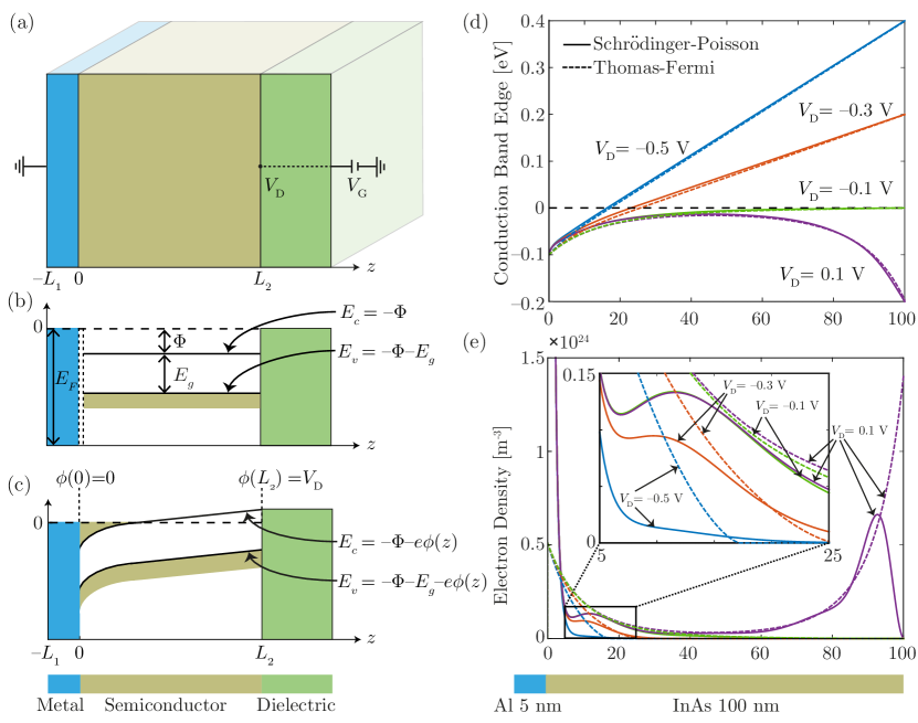
We consider the hybrid device depicted in Fig. 1(a), showing a layered structure consisting of metal, semiconductor and dielectric with translational invariance in the plane. The device is characterized by two boundary conditions for the electrostatic potential : (i) the metal layer is assumed to be a grounded conductor with , (ii) the rightmost edge of the dielectric is in contact to a back gate with . For our self-consistent modeling we focus only on the metal and semiconductor region of the device, and in this case (ii) is replaced by a scaled back gate voltage at the semiconductor-dielectric interface. In fact, depending on the choice of the dielectric layer, and may differ by very little Gat .
We wish to determine the conduction band edge and charge density profile in our device. The idea behind our approach is shown in the band diagrams of Figs. 1(b) and (c). We assume that the Fermi level of the metal layer (dashed line) sets the chemical potential of the hybrid system and choose this as our reference energy. The distance between the Fermi level of the metal and its conduction band edge is determined by its Fermi energy, , which we set to the bulk Al value, i.e. (Ashcroft and Mermin, 1976). Before contact (Fig. 1(b)), the conduction band edge of the semiconductor is assumed to be below the Fermi level of the metal corresponding to a positive difference between the electron affinity of the semiconductor and work function of the metal, that is . The results turn out to be very sensitive to this value and here we start by studying the case when the value of this experimentally not yet fully resolved parameter is .
When the metal and semiconductor layer are contacted (Fig. 1(c)), the band edges of the semiconductor will bend due to the presence of charges that are transferred from the metal into the semiconductor conduction band. We assume that only the conduction band electrons contribute to the band bending in the semiconductor, thus disregarding the presence of the valence band electrons. This approach is valid for the low-temperature range of interest, where (Winkler, 2003). Furthermore, we must restrict ourselves to back gate voltages where the valence band edge of the semiconductor stays below the Fermi level of the metal; otherwise the band bending would lead to the formation of an unwanted hole pocket near the semiconductor dielectric interface. As indicated in Fig. 1(c), this condition is satisfied as long as , which thus defines a lower bound for values of that we can apply.
We determine the band edge and charge density profiles for our device using both a Thomas-Fermi approximation and a self-consistent Schrödinger-Poisson method. Both of these methods rely on determining through Poisson’s equation, which is solved only in the semiconductor region of our device
| (1) |
Here denotes the dielectric constant of the semiconductor, which we set to corresponding to InAs, while denotes the charge density of conduction band electrons. The boundary conditions for Eq. (1) are the previously described electrostatic boundary conditions, i.e. and .
II.2 The Thomas-Fermi approach
The Thomas-Fermi approximation relies on the assumption that the electronic charge density is given by the same expression as the standard result for a homogenous 3D electron gas
| (2) |
Here denotes the local Fermi energy in the semiconductor, which is determined by the offset between the conduction band edge and Fermi level of the metal, i.e. , while denotes the effective mass of the semiconductor, which we set to corresponding to zincblende InAs (Winkler, 2003).
The Thomas-Fermi approach further combines Eq. (2) with Poisson’s equation (1). This is most conveniently done via the introduction of the following rescaled quantites: (i) electrostatic potential and (ii) coordinate . Here we defined the Thomas-Fermi length-scale , where denotes the charge density obtained in Eq. (2) for . With the help of these rescaled quantities, Poisson’s equation (1) may be rewritten in the following dimensionless form
| (3) |
The boundary conditions for follows from the boundary conditions for , i.e. and . We solve Eq. (3) using standard numerical techniques for non-linear differential equations.
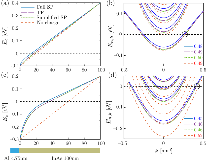
Figs. 1(d) and (e) show the result of a Thomas-Fermi calculation (dashed lines) of the conduction band edge and charge density profile in an Al-InAs device for several values of . The calculation was done with thicknesses of and for the Al and InAs layers, respectively. We find that a triangular well forms near the Al-InAs interface due to band bending, which leads to charge accumulation close to the superconductor. Furthermore, for a positive value of , we find that electrons also accumulate near the dielectric away from the superconductor, thus leading to puddles with reduced superconductor-semiconductor hybridization. This situation is undesired since the hole puddle would give an ungapped region in the semiconductor and introduce quasiparticle poisoning to the Majorana device.
II.3 The Schrödinger-Poisson approach
The Schrödinger-Poisson approach is based on self-consistently solving Poisson’s equation (1) together with the following Schrödinger equation
| (4) |
The plane translational invariance allows us to consider a fixed in-plane wavevector of magnitude . The quantities and denote the effective mass and band edge of the hybrid system with the latter given by (see Fig. 1(c))
| (5) |
The boundary conditions for the differential equation (4) are the hard-wall boundary conditions, i.e. . We solve it using a standard finite difference approach, explained in Appendix A.
To obtain the self-consistent solution of Eqs. (1) and (4) we need the electronic charge density which is found by integrating over the occupied eigenstates of Eq. (4), according to
| (6) |
with denoting the Heaviside step function. We calculate from the above by solving Eq. (4) for many different values of and subsequently evaluating the integral numerically.
Figs. 1(d) and (e) show the results of a Schrödinger-Poisson (solid lines) calculation of the conduction band edge and charge density profile with the same parameters as the previously described Thomas-Fermi calculation. The two approaches yield remarkably similar results for the band edge and quite similar results for the charge density profile. The strongest deviation for the latter appears at the metal-semiconductor interface, where the Thomas-Fermi result approaches the value predicted by Eq. (2), while the value obtained using the Schrödinger method rises steeply due to the hybridization with the Al layer.
II.4 The hybrid band structure
Having determined the band bending profile, we proceed to investigate the hybrid band structure obtained from solving the Schrödinger equation (4). Here we focus on results where was obtained using the Schrödinger-Poisson approach, but in Appendix B, we also compare these to results based on simpler approximations including the Thomas-Fermi approach.
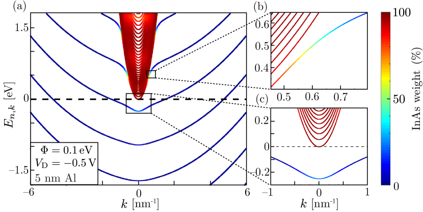
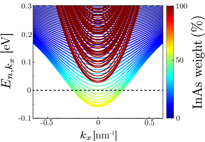
We first address the overall character of the bands based on the results displayed in Fig. 2 showing both as well as the weights in the InAs region of the corresponding wave functions . We have chosen to include negative values of , such that the presented band structure corresponds to a cut through the 2D paraboloidal band structure of the system. From the large-scale zoom provided by Fig. 2(a) it is evident that the band structure is composed mainly of segments with negligible InAs weight corresponding to states localized in the Al region. It however also contains a dense region of band segments with high InAs weight corresponding to states which are predominantly localized in the InAs region. Strikingly, band segments with strong superconductor-semiconductor hybridization, i.e. with substantial weight of both InAs and Al, occur rarely as shown in Fig. 2(b). We present in the next section an analytical approach for predicting when bands have substantial hybridization.
As discussed in Sec. IV, band segments with mixed weights are in fact crucial for the realization of robust Majorana zero modes. They correspond to states with both a strong SOC strength and sizeable superconducting gap, proportional to the Al character of the band, given by the weight . Below we therefore investigate whether it is possible to obtain states of this character at the Fermi level. Furthermore, other bands that cross the Fermi level should not have large InAs weight () at the Fermi energy since this would give rise to a soft gap.
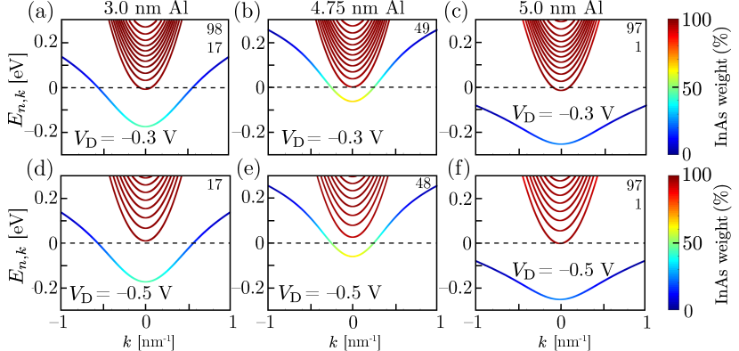
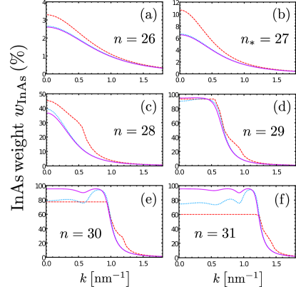
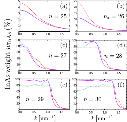
To investigate the conditions for having states with mixed weights at the Fermi energy, we address the effects of varying the effective gate voltage and Al layer thickness , which are both parameters that can be tuned experimentally. Our results are summarized in Fig. 3, where the top right corner of each subfigure shows the weight at the Fermi level of the crossing bands. We focus on negative values of for which all states are located close to the superconductor-semiconductor interface and restrict ourselves to gate voltages above which, as previously discussed, defines a lower bound for values of .
Figs. 3(b) and (e) show that it is indeed possible to obtain a situation where a band with strong hybridization crosses the Fermi level, while InAs-like bands are kept above the Fermi level. Evidently this is obtained by tuning the Al layer thickness, which delicately determines the position and hybridization of the lowest Al-like band. In contrast, the hybridization of the bands responds more weakly to changes in . From Fig. 3 one can verify that lowering the gate voltage has the expected effect of pushing up all the InAs-like bands, thereby depopulating states which would otherwise lead to a soft bulk gap. Nonetheless, gating appears only to affect the position of these bands, while their hybridization profile remains practically unchanged. In contrast, states with strong coupling to the superconductor essentially remain at the same energies. The reason for this is that the semiconductor component of the wavefunction of a strongly hybridized state is concentrated near the superconductor-semiconductor interface, where the superconductor screens the presence of the gate electrode.
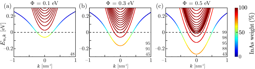
To conclude this section, we investigate the effects of varying the parameter , which so far has been set to the value . Our results are summarized in Fig. 4, which displays the band structure at the Fermi level for different values of using the parameters and (chosen to achieve strong hybridization at the Fermi level). The results show that increasing values of lead to the emergence of more InAs-like bands below the Fermi level, thereby leaving several InAs-like states at the Fermi energy with negligible coupling to the superconductor. This is not surprising, since effectively determines the depth of the quantum well at the superconductor-semiconductor interface, but it does appear contradictory to reported experimental measurements on hybrid Al-InAs structures which suggest a regime in which all states at the Fermi energy are strongly coupled to the superconductor. In our framework such a regime is achievable only with a small value of e.g. , which thus explains our motivation for originally choosing this value for . It should, however, be emphasized that this chosen value is somewhat smaller than found by recent angle resolved photoemission spectroscopy (ARPES) experiments ARP . The ARPES measurement were done for a bulk zincblende structure, but the relevant structure for the nanowire systems is wurtzite where the electron affinity is known to be 0.1 eV smaller. Therefore, using 0.1 eV for nanowire systems could be consistent with these experiments. Moreover, it should be noted that these values significantly differ from the bulk value for the difference between the work function of Al and electron affinity of InAs (Eastment and Mee, 1973; Gobeli and Allen, 1965) .
III Analytical approach to hybridization
III.1 Effective-square versus triangular well model
To shed light on the factors determining the degree of the superconductor-semiconductor hybridization, we proceed with studying a simpler and analytically tractable model. This model is obtained by replacing the triangular potential in the semiconductor with a rectangular well. This is applicable in the case of a large negative and the situation corresponds to the one depicted in Fig. 1(b), with the only difference that the physical width of InAs is replaced by an effective width , roughly given by the length for which the triangular potential crosses the Fermi level. In fact, by comparing the reconstructed band structures of the two models, we find that they share the same qualitative features. To illustrate this connection, we compare in Fig. 5 (6) the InAs weights obtained via the Schrödinger-Poisson method for parameters , and (), with the ones calculated using the square potential for . In the same plots we also include the weights calculated via employing the approximate analytic expressions to be discussed in the next paragraph. One observes that, given the way is chosen, the weights obtained using these two models are in good agreement for energies near the Fermi level and begin to deviate for energies which lie above the Fermi level. This deviation mainly happens for small since the discrepancy is related to the sensitivity of the InAs-like bands to the electric field. The agreement allows us to extract approximate analytical expressions describing the hybridization characteristics using the square-well model.
III.2 Square-well model and hybrid band structure
The wave functions in both regions are given by sinusoidal functions with wave numbers and . For a fixed they have the form
| (7) | |||||
| (8) |
Due to the broken translational invariance along the direction, the wave numbers are determined by the energy
| (9) |
Here and denote constants that will be found via the normalization and appropriate matching conditions at the interface , respectively. The wave function matching yields the transcendental equation:
| (10) |
The above equation supports two types of solutions characterized by: (i) and and (ii) . The first type describes dispersive solutions in Al which leak inside InAs within a width . The second type of solutions correspond to states which disperse in .
III.3 The band structure features
Let us first discuss the bands which originate mainly from the pure Al bands. These become very weakly modified by the InAs conduction band considered here, and belong to the first type of solutions mentioned earlier possessing an imaginary . In fact, wave functions of this type will penetrate only a very small distance into the InAs region. For these deep bands, one has , corresponding to the Al layer being an infinite square well with energies
| (11) |
For the approximate energy dispersions of these bands see Appendix C.
There are such bands where is defined by
| (12) |
For and () we find () which corresponds to (). For these weakly modified Al-like bands, the penetration depth into the semiconductor layer is approximately given by
| (13) |
For the above parameters and (), we find that () at . At finite the penetration length becomes even smaller which becomes evident from the equation above. Finally, the InAs weight of such a band is approximately given by the expression
| (14) |
The numerical methods employed earlier for retrieving Figs. 5 and 6 confirm that the InAs weight increases with , and for it attains values of the order of . In the same figures we have also calculated the weight via the approximate Eq. (14). We find that the InAs weight, while still reasonably low, is overestimated by this approximate formula. The same happens for .
In contrast to the low degree of hybridization achieved for the typical device parameters considered here when , for it is possible to find bands that depending on the value of exhibit strong hybridization. We have studied the structure of the solutions of the transcendental equation (10) and found that also the bands above have a one-to-one correspondence to the pure Al bands, in accordance with Ref. Heine (1965). However, they significantly differ compared to the pure Al bands, since they become strongly modified in the presence of InAs, especially for small . Therefore, a band with is generally divided into three -space regions for which or . See for instance Fig. 7.
For large the new bands resemble the weakly modified Al bands with , since the pure InAs bands are concentrated in the small region. In most of the cases, the bands are thus Al-like as and become InAs-like as . In between, new band structure segments appear upon hybridization, which glue the pure Al and InAs bands together. These are characterized by . Such segments are depicted in Fig. 2(b,c) and illustrated with dashed (cyan) ellipses in Figs. 7(a,b). In general, they appear for , with given by the inequalities:
| (15) |
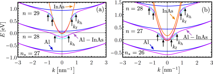
It is possible that and one obtains the situation of Figs. 2(c), 3(c) and 7(a) of an Al-like band with additionally strong InAs character for small . Essentially, the th pure Al band is pushed downwards after contact with InAs, so that a new band now appears below the location of the pure InAs bands. See band in Fig. 7(a). This occurs if the following condition is satisfied for the last Al-like band (meaning for )
| (16) |
This type of gluing band segments, appearing only for , possesses an InAs weight given approximately by (see Appendix C)
| (17) |
For and the length satisfies the approximate relation
| (18) |
Based on Figs. 5 and 6 one infers that it is precisely these band segments which have mixed Al-InAs character and exhibit strong hybridization. Thus, in order to ensure the robustness of the Majorana device one should maximize the difference and ensure that these segments cross the Fermi level. Strikingly, at the level of approximation considered here, the penetration depth, InAs weight and energy of these segments do not depend on . This also implies a very weak dependence on the back-gate potential and , thus, explaining the findings of Fig. 3.
The above discussion has already covered the bands with for all , as well as the band segments for for . We proceed with investigating the properties of the band segments appearing for which primarily possess InAs character. At this point we distinguish two scenarios, corresponding to Figs. 7(a,b), depending on whether a new band (scenario I) appears below the pure InAs bands or not (scenario II).
Scenario I When the condition of Eq. (16) is satisfied, a band appears below the pure InAs levels, as in Fig. 7(a). In this case we find at higher energies hybridized InAs-like bands with , and modified energies given by
| (19) |
where we introduced the InAs energy levels
| (20) |
and defined a hybridization coefficient
| (21) |
The above approximation holds for bands satisfying , while for higher energies different approximations apply. See Appendix C. The InAs weights for these bands are approximately given by
| (22) |
As it can be seen from Figs. 5 and 6, the Al-content of these bands is practically negligible, at least for the parameter values considered here. It is desirable that these band segments acquire a sizeable superconducting gap and get pushed to higher energies, and thus enhance the device protection against quasiparticle poisoning. To achieve this goal one could use a metal with a smaller Fermi energy in order to reduce .
Scenario II So far we have examined the situation in which the th pure Al level does not get glued to a pure InAs level for , but instead it is pushed downwards in energy yielding a band below the pure InAs ones. This is the case of Fig. 7(a). However, within the present model a slight modification of by can lead to a different situation in which the condition of Eq. (16) is not satisfied. As a result one finds a different approximate expression for the InAs weight of the levels above and small , i.e. . In this case, corresponding to Figs. 3(b,e), 4(a) and 7(b), the pure Al levels become glued with the pure InAs ones via appropriate segments of mixed character. While the InAs weight and of these segments appearing for are given by the equations discussed earlier, the expressions describing the InAs-like parts living in become modified. We find that for the energy of the segments defined for and read (see Appendix C for details)
| (23) |
and the InAs weight is given by the simple -independent formula
| (24) |
We note that for the weight is . From Fig. 6 we find that this result agrees well with the corresponding Schrödinger-Poisson calculation for . As increases one finds stronger deviations because for higher energies the differences between the square and triangular wells become more pronounced. In the next paragraph we show how to extend our approach and obtain an improved agreement with the Schrödinger-Poisson results.
III.4 Extended square-well model and fit to the Schrödinger-Poisson solution
The above conclusions can help us understand the obtained band structure when the electrostatic effects, introduced by a non-zero , are taken into account. The strongly hybridized bands have a relatively short decay length inside InAs and weakly feel the electrostatic potential. On the other hand, the InAs-like bands are extended over a larger region and are prone to the gate-induced electric fields. The effect of the triangular well is to broaden the effective width for energies above the Fermi level. In fact, for a band with index consisting of an InAs band with energy ( or ) one can define an effective energy dependent , given by
| (25) |
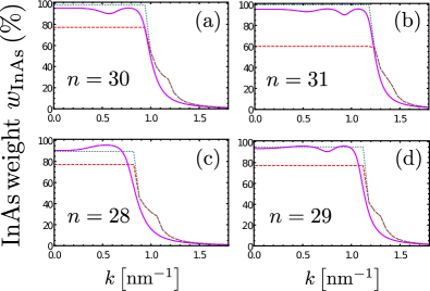
since these bands appear for small . Here denotes the electric field in the system, which is non-zero only in the semiconductor’s region. For we find that . By appropriately varying depending on the band, we obtain a very good agreement with the Schrödinger-Poisson results as shown in Fig. 8.
IV Effective parameters for Majorana devices
Having solved the electrostatics and studied the metal-semiconductor hybridization in detail, we now discuss its consequences for the realization of Majorana zero modes. The starting point for our analysis is the Bogoliubov-de Gennes Hamiltonian in the presence of the self-consistent potential determined above, see Eq. (5), with added terms due to the Zeeman coupling, Rashba SOC and spin-singlet superconductivity. Using that the problem is translationally invariant in the plane, we write the Hamiltonian in -space as
| (26) | |||
where () are Pauli matrices operating in spin (electron-hole space). Furthermore, denotes the -factor of the hybrid system, which is set to in the Al region and (Winkler, 2003) in the InAs region. The magnetic field is in-plane such that orbital effects play little role. The term is the Rashba SOC strength, which is given approximately by (Winkler, 2003)
| (27) |
with
| (28) |
The final component entering Eq. (26) is the superconducting order parameter which is non-zero only in Al. For bulk Al, .
If we assume large negative back gate voltages leading to a constant electric field in the semiconductor of the order of , as estimated from the results in Fig. 1(d), the strength of the Rashba SOC in Eq. (27) becomes . For we find , and .
The effective superconducting gap, -factor and chemical potential () enter into the condition determining the transition of an Al-InAs nanowire into the topological superconducting phase. When a single confinement channel of the nanowire hybrid band structure (see Fig. 9) crosses the Fermi level, the topological criterion reads . The dependence of these parameters on the InAs weight, for which we obtained analytic expressions in the previous section, can be employed to indirectly infer the role of physical parameters such as the Al width, gate voltage and band offset. On the other hand, the effective mass () and SOC strength determine the Majorana decay length , which further controls the resulting energy splitting and oscillations of overlapping Majorana zero modes in finite-sized nanowires Cheng et al. (2009); Rainis et al. (2013); DasSarma et al. (2012); Mishmash et al. (2016). The self-consistent Schrödinger-Poisson investigation of these effects in such a nanowire setup would require a full 3D simulation, which is a task beyond the scope of the present paper. Nevertheless, we can provide a rough estimate for . According to Ref. Mishmash et al., 2016 we are in the case of weak SOC, which for the above parameter values implies . Finally, note that the inclusion of electrostatic effects can lead to a suppression or vanishing of the Majorana oscillations Dominguez et al. (2017); Esc , through the zero-energy pinning of the state originating from the overlapping Majorana zero modes.
To this end, we note that in our self-consistent electrostatics analysis we neglected the SOC, Zeeman and superconducting contributions. We have verified that the inclusion of the SOC term in the self-consistent Schrödinger-Poisson problem does not significantly modify the obtained results. This also holds for both magnetic field and superconducting energy scales which constitute the smallest energy scales in the problem. Therefore, one could use the presented results for the band edge profiles and hybridization degrees for further modeling the physics of experimentally realized Majorana devices.
V Discussion and conclusions
We have assessed the role of band bending and superconductor-semiconductor hybridization in Majorana devices by studying a planar, gated Al-InAs interface. Our results were based on a self-consistent Schrödinger-Poisson approach, which revealed that the band bending leads to an approximately triangular quantum well along with a charge accumulation layer at the Al-InAs interface. We also compared the Schrödinger-Poisson calculation with a Thomas-Fermi approach which ignores the hybridization and found remarkably similar results for the band bending. This can be useful for future calculations since one can use the computationally faster Thomas-Fermi approach to determine the self-consistent potential and then solve the Schrödinger equation in this potential.
The character of the superconductor-semiconductor hybridization was addressed by calculating the band structure of the hybrid system and investigating its response to varying the Al layer thickness, gate voltage and native band offset. Our main finding is that the system parameters may be tuned to a situation as shown in Fig. 3(e) where a band with strong superconductor-semiconductor hybridization crosses the Fermi level, while higher levels of predominately InAs character stay above it. Such a situation is ideal for inducing superconductivity in the InAs region, which requires strong hybridization with the Al region, while simultaneously keeping out the InAs-like bands, which would give rise to a soft superconducting gap.
To back our numerical findings, we analyzed the superconductor-semiconductor hybridization using an analytical approach showing that the hybridization is only sizable when there is resonance between the uncoupled Al and InAs bands. This behavior might seem surprising given the absence of a barrier between the materials, and it appears to be a result of mismatch of the wavefunctions in the metal square well and triangular semiconductor well.
The conditions for having the ideal situation shown in Fig. 3(e) turns out to be extremely sensitive to the Al layer thickness, while a far weaker dependence on the gate voltage was found. As a matter of fact, in the regime of interest, the sensitivity to the Al width manifests itself through an alternating pattern of high and low values of the hybridization degree. Thus, the strong hybridization is not restricted to a single window of Al widths, but rather, it appears in a periodic fashion. An obvious question to address is whether the observed sensitivity persists for thicknesses much larger than which is a width typically employed in experiments. By investigating Al thicknesses such as 50nm and 60nm, we have found that a significantly better hybridization of the pure InAs-like bands can be achieved but that the observed sensitivity on the Al thickness remains. We expect that this sensitivity will persist, until the pure Al-level splitting for energies near the semiconductor’s band edge is comparable to the splitting of the pure InAs-levels. For the parameters employed in the case of Fig. 3(e) we find that for the respective values of Al-width . Thus, it appears that quite thick Al layers are required to soften the sensitivity in question. Note, that, in experiments small Al thicknesses are preferred in order to enhance the critical magnetic field at which the device becomes non-superconducting.
We have seen that the hybridization and the number of bands below the Fermi energy depend strongly on the thickness of the Al layer and therefore one expects that disorder such as variations by even a single monolayer of the deposited Al layer could have strong effects. Likewise, if a nanowire structure is formed out of the quasi-2D system studied here, a non-regular cross section could give qualitatively different results from what we found for the 2D translationally invariant setup. Moreover, the strong dependence on Al thickness also raises the question whether a more microscopic description (for example a tight-binding model of the Aluminum) would give a different result. We speculate that the details will naturally be different but also that the sensitivity to thickness remains because of the large mismatch of energy scales between the two materials. Given the extreme sensitivity to the Al width, as discussed above, one may wonder how this is consistent with the experimental data which have been interpreted as signatures of induced topological superconductivity Mourik et al. (2012); Deng et al. (2016); Albrecht et al. (2016); Nichele et al. (2017); Zhang et al. (2018); Sau , because it would require atomically-flat Al along the whole length of the nanowire which seems unlikely to be case. However, the sensitivity may be softened by width variations on short length scales which could average out the hybridization degree. The length scale of roughening of the Al surface depends on growth conditions, semiconductor morphology and lattice matching. An example of a very highly ordered Al surface is when it is grown on lattice matched planar GaSb/InAs based materials where the interfacial domain matching with Al can be highly ordered. In this case the Al can follow the semiconductor surface morphology over several microns (verified by atomic force microscopy on structures with up to 300nm step size). But for most hybrid materials the roughness take place on much smaller length scales, down to the few nanometer scale. This roughness may be responsible for the proposed averaging. Therefore, both the effect of disorder and a more detailed band structure are natural questions for further research.
Another important parameter is how the metal Fermi level aligns with the semiconductor conduction band, see Fig. 1. Here we have used in the range , which is supported by recent experiments ARP , but not by known bulk values. Therefore, it could be that there is some surface chemistry that still needs to be resolved before a more complete understanding of these structures can be reached.
In conclusion, devices based on Al-InAs or similar material combinations are indeed promising candidates for Majorana physics and several experiments have already shown signatures of Majorana zero modes. However, based on the analysis here it seems to require a fine balance between several parameters, such as the metal thickness and band alignments. In our simulations the effect on gate voltage is very limited when it comes to the degree of hybridization, while it predominantly affects the position of the InAs-like bands. Disorder effects might help in relaxing these conditions. Studying these effects would require a 2D simulation, which we intend to pursue in future works. Experimentally, there seems to be a stronger dependence on gate voltage which could be due to the gate coupling inhomogeneously to the structure. A better understanding of this would require a full 3D self-consistent simulation.
At the time of submission two other works addressing Schrödinger-Poisson calculations for superconductor-semiconductor hybrid structures appeared Ant ; Woo . We find that our results on the hybridization are in a good agreement with those obtained in these works using numerical methods. The primary interest of Refs. Ant, ; Woo, is to explore aspects of the topological phase diagram of nanowires. Specifically, the authors of Ref. Ant, discuss the influence of gating on the effective -factor, while Ref. Woo, focuses on efficient numerical methods for solving the Schrödinger-Poisson problem, as well as, on the electrostatic effects on the Majorana oscillations. In the present paper, we have put emphasis on understanding in detail the superconductor-semiconductor hybridization and investigated the sensitivity of the degree of hybridization upon varying key parameters (e.g., Al thickness). We have also derived approximate analytic expressions enabling experimental predictions.
Acknowledgements
We would like to thank A. Akhmerov, A. Antipov, K. Björnson, M. Hell, R. Lutchyn, S. Schuwalow, S. Vaitiekénas, A. Vuik, G. Winkler, and M. Wimmer for useful discussions. This work was supported by the Danish National Research Foundation, by the Microsoft Station Q Program and by the European Research Commission, project HEMs-DAM no.716655, starting grant under Horizon 2020..
Appendix A Numerical methods
A.1 The Schrödinger equation
The Schrödinger equation (4) is solved on a 1D grid using the finite difference approximation:
| (29) |
Here denotes the average value of the effective mass on the two grid points i and i+1. Since the Fermi wave length of the metal is orders of magnitude smaller than that of the semiconductor it is advantageous to make the discretization more coarse in the semiconductor region. The results presented in this work were obtained using a fixed grid spacing of 0.1 Å in the Al region and 2 Å in the InAs region. To obtain the solutions to the system of Eq. (29), we solve it as an eigenvalue equation. We enforce hard-wall boundary condition by setting the wave functions to zero at the ends of the 1D grid.
A.2 Obtaining the self-consistent solution
Our Schrödinger-Poisson approach relies on self-consistently solving Eqs. (1), (4) and (6). For this we employ a simple mixing scheme, where the input electrostatic potential used in each iteration is a simple mixing of the input and output electrostatic potential of the previous iteration
| (30) |
In our calculations we used . For the initial input, we use . While the authors of Ref. Vuik et al. (2016) have shown that more sophisticated mixing schemes such as Anderson mixing leads to a faster convergence, we find that the simple mixing scheme above provides reasonably fast convergence within the first 50-100 self-consistent iterations.
Appendix B Influence of band bending on the hybridization
The hybrid band structures shown in Sec. II.4 were obtained using obtained from the Schrödinger-Poisson approach. This procedure is computationally demanding since it requires solving Eq. (4) a larger number of times within each self-consistent iteration when calculating the electronic density from Eq. (6). In this section, we explore the consequences of employing simpler and computationally faster approaches for calculating . Specifically, we compare the results of Sec. II.4 to those obtained when is determined by:
-
1.
The Thomas-Fermi approach described in Sec. II.2.
-
2.
A simplified Schrödinger-Poisson approach, where Eq. (4) is solved only in the InAs region with boundary conditions . In this case the wave functions are independent of and the density in the semiconductor region is found by integrating over the 2D density of states for each subband yielding
(31) -
3.
With in the semiconductor, i.e. neglecting band bending due to charge in the InAs such that
(32)
Our results are summarized in Fig. 10 where we show both the resulting band bending and the band structure plots from the different approaches for and . We have here chosen parameters such that a strongly hybridized band crosses the Fermi level, and the corresponding InAs weights at the Fermi energy (indicated by the circle) are shown in the bottom left corners of Figs. 10(b) and (d).
When (Figs. 10(a,b)) the density in the InAs region is low, and the band edges exhibit only a slight bending, staying close to the constant slope found without density in the semiconductor. Notably the strongest bending is found when the full Schrödinger-Poisson approach is employed. This is due to the hybridization with the Al which induces a large electron density close to the Al-InAs interface (see Fig. 1(d)). In the case , the band bending profiles are much stronger and deviate substantially from the solution without charge. Thus, the strongest bending is found from the full Schrödinger-Poisson approach, but both Thomas-Fermi and simplified Schrödinger-Poisson methods yield similar results.
The same conclusion holds for the band structure plot of Fig. 10(d). Here the band structures obtained with band bending are reasonably similar, while the one obtained with constant slope evidently contains additional bands below the Fermi level due to the more shallow band profile. Interestingly, it appears that the weight at the Fermi energy of the strongly hybridized band is only weakly dependent on the exact band bending profile and all approaches yield comparatively similar results.
Appendix C Analytical approach to hybridization
In this appendix, we demonstrate how to obtain approximate analytical expressions for the band structure properties of the square-well model of Sec. III.2. We start from Eq. (10) and rewrite the transcendental equation as
| (33) |
or bring it to its inverted form
| (34) |
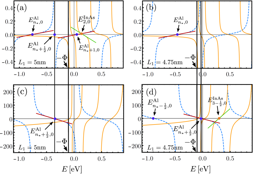
Fig. 11 depicts the functions of the l.h.s. (dashed blue) and r.h.s. (solid gold) of Eqs. (33) and (34) for , , , and Al width and , respectively. The energy eigenstates of the hybrid band structure are given by the crossing points of the two functions. For low energies we have essentially solutions corresponding to isolated Al. Instead, for energies in the vicinity of the pure InAs levels, we find solutions emerging from the hybridization of InAs and Al. In Fig. 11 the top and corresponding bottom panels, i.e. (a,c) and (b,d), lead to identical solutions. Nevertheless, we have included them both since, depending on the energy regime, it is more convenient to employ the inverted (34) instead of the direct transcedental equation (33).
The aim is to Taylor expand the l.h.s. or/and r.h.s., of the respective transcedental equation employed, about zero. Depending on the case, one performs a linear or quadratic Taylor expansion. If we work with Eq. (33) we can expand the l.h.s. as follows
| (35) |
with the energy shift being measured from a pure Al level, which yields a zero tangent since . A similar method is followed if we want to expand the r.h.s. of the same equation about the pure InAs levels.
If it is instead preferable to employ Eq. (34), then one should expand about a zero of the respective l.h.s. or r.h.s.. For instance, if we wish to expand the l.h.s. about a zero of the cotangent obtained for
| (36) |
we have
| (37) |
Here the energy shift is measured relative to the th pure Al level. In reality there is no such a pure Al level before contact with InAs, but this notation is convenient because it reflects that we are focusing on energy eigenstates which appear due to the Al-InAs hybridization. One can further expand the r.h.s. about the th pure InAs level, with , in a similar fashion.
Before proceeding with obtaining the various approximate analytical expression discussed in the text, let us remark that our approach generally holds for the case of small Al widths where the spacing of the pure Al levels is much larger that the spacing of the pure InAs levels. Our approximation further holds for arbitrary values of . However, it can modify the number of Al-InAs bands for which our method is valid.
C.1 Solutions with and
After applying the matching conditions, we find that the wave function for such a solution with has the approximate form
| (38) |
for and
| (39) |
for . The InAs and Al weights are defined as
| (40) |
We first discuss the weakly modified pure Al levels, with for all and for . In this case we start from Eq. 33. We linearize the l.h.s. about , consider , and set on the r.h.s.. In Figs. 11(a,b) we show details for the level. We find that the eigenenergies approximately read
| (41) | |||
C.2 Solutions with and
After applying the matching conditions, we find that the wave function for such a solution with has the approximate form
| (43) |
for and
| (44) |
for with the weights discussed in the main text. These solutions appear for defined in Sec. III. One distinguishes two scenarios I and II.
Scenario I In this case we use Eq. (33) and linearize both sides. We linearize the l.h.s. about the level and the r.h.s. about the level. See Fig. 11(a) for . This approximation led to Eqs. (19) and (22), and holds as long as the linear approximation of the l.h.s. is valid, i.e. .
Scenario II In this case we use Eq. (34) and linearize both sides. We linearize the l.h.s. about the level and the r.h.s. about the level. See Fig. 11(d) for . This approximation led to Eqs. (23) and (24). Note that this approximation holds as long as the linear approximation of the l.h.s. is valid, i.e. . In this case, for we are on the borderline of our approximation’s validity. For larger , e.g. we have to expand up to quadratic order the r.h.s. in order to obtain a good approximate solution, and in this case the energy reads
| (45) |
which is applicable for bands satisfying . The approach can be extended to higher energies by separating the energy interval in regions where the direct or inverted transcendental equation is best.
References
- (1) S. M. Sze and K. K. Ng, Physics of Semiconductor Devices, 3rd Edition, (Wiley-Interscience, New Jersey, 2006).
- Bardeen (1947) J. Bardeen, Surface states and rectification at a metal semi-conductor contact, Phys. Rev. 71, 717 (1947).
- Heine (1965) V. Heine, Theory of Surface States, Phys. Rev. 138, A1689 (1965).
- Beenakker (2013) C. W. J. Beenakker, Search for Majorana fermions in superconductors, Annu. Rev. Condens. Matter Phys. 4, 113 (2013).
- Alicea (2012) J. Alicea, New directions in the pursuit of Majorana fermions in solid state systems. Rep. Prog. Phys. 75, 076501 (2012).
- Leijnse and Flensberg (2012) M. Leijnse and K. Flensberg, Introduction to topological superconductivity and Majorana fermions, Semicond. Sci. Technol. 27, 124003 (2012).
- Aguado (2017) R. Aguado, La Rivista del Nuovo Cimento 40, 523 (2017).
- Lutchyn et al. (2018) R. M. Lutchyn, E. P. A. M. Bakkers, L. P. Kouwenhoven, P. Krogstrup, C. M. Marcus, and Y. Oreg, Nature Review Materials 3, 52 (2018).
- Kitaev (2001) A. Y. Kitaev, Unpaired Majorana fermions in quantum wires, Phys. Usp. 44, 131 (2001).
- Ivanov (2001) D. A. Ivanov, Non-Abelian Statistics of Half-Quantum Vortices in p-Wave Superconductors, Phys. Rev. Lett. 86, 268 (2001).
- Alicea et al. (2011) J. Alicea, Y. Oreg, G. Refael, F. von Oppen, and M. P. A. Fisher, Non-Abelian statistics and topological quantum information processing in 1D wire networks, Nat. Phys. 7, 412 (2011).
- Aasen et al. (2016) D. Aasen, M. Hell, R. V. Mishmash, A. Higginbotham, J. Danon, M. Leijnse, T. S. Jespersen, J. A. Folk, C. M. Marcus, K. Flensberg, and J. Alicea, Milestones Toward Majorana-Based Quantum Computing, Phys. Rev. X 6, 031016 (2016).
- Plugge et al. (2017) S. Plugge, A. Rasmussen, R. Egger, and K. Flensberg, Majorana box qubits, New Journal of Physics 19, 012001 (2017).
- Karzig et al. (2017) T. Karzig, C. Knapp, R. M. Lutchyn, P. Bonderson, M. B. Hastings, C. Nayak, J. Alicea, K. Flensberg, S. Plugge, Y. Oreg, C. M. Marcus, and M. H. Freedman, Scalable designs for quasiparticle-poisoning-protected topological quantum computation with Majorana zero modes, Phys. Rev. B 95, 235305 (2017).
- Mourik et al. (2012) V. Mourik, K. Zuo, S. M. Frolov, S. R. Plissard, E. P. A. M. Bakkers, and L. P. Kouwenhoven, Signatures of Majorana fermions in hybrid superconductor-semiconductor nanowire devices. Science 336, 1003 (2012).
- Krogstrup et al. (2015) P. Krogstrup, N. L. B. Ziino, W. Chang, S. M. Albrecht, M. H. Madsen, E. Johnson, J. Nygård, C. Marcus, and T. S. Jespersen, Epitaxy of semiconductor-superconductor nanowires, Nat. Mat. 14, 400 (2015).
- Chang et al. (2015) W. Chang, S. M. Albrecht, T. S. Jespersen, F. Kuemmeth, P. Krogstrup, J. Nygård, and C. M. Marcus, Hard gap in epitaxial semiconductor-superconductor nanowires, Nature Nanotechnology 10, 232 (2015).
- Deng et al. (2016) M. T. Deng, S. Vaitiek, E. B. Hansen, J. Danon, M. Leijnse, K. Flensberg, P. Krogstrup, and C. M. Marcus, Majorana bound state in a coupled quantum-dot hybrid-nanowire system, Science 354, 1557 (2016).
- Albrecht et al. (2016) S. M. Albrecht, A. P. Higginbotham, M. Madsen, F. Kuemmeth, T. S. Jespersen, J. Nygård, P. Krogstrup, and C. M. Marcus, Exponential Protection of Zero Modes in Majorana Islands, Nature 531, 206 (2016).
- Nichele et al. (2017) F. Nichele, A. C. C. Drachmann, A. M. Whiticar, E. C. T. O’Farrell, H. J. Suominen, A. Fornieri, T. Wang, G. C. Gardner, C. Thomas, A. T. Hatke, P. Krogstrup, M. J. Manfra, K. Flensberg, and C. M. Marcus, Scaling of Majorana Zero-Bias Conductance Peaks, Phys. Rev. Lett. 119, 136803 (2017).
- Zhang et al. (2018) H. Zhang, C.-X. Liu, S. Gazibegovic, D. Xu, J. A. Logan, G. Wang, N. van Loo, J. D. S. Bommer, M. W. A. de Moor, D. Car, R. L. M. O. het Veld, P. J. van Veldhoven, S. Koelling, M. A. Verheijen, M. Pendharkar, D. J. Pennachio, B. Shojaei, J. S. Lee, C. J. Palmstrom, E. P. A. M. Bakkers, S. D. Sarma, and L. P. Kouwenhoven, Quantized Majorana conductance, Nature 556, 74 (2018).
- Suominen et al. (2017) H. J. Suominen, M. Kjaergaard, A. R. Hamilton, J. Shabani, C. J. Palmstrøm, C. M. Marcus, and F. Nichele, Zero-Energy Modes from Coalescing Andreev States in a Two-Dimensional Semiconductor-Superconductor Hybrid Platform, Phys. Rev. Lett. 119, 176805 (2017).
- Vaitiekenas et al. (2018) S. Vaitiekenas, M. T. Deng, J. Nygård, P. Krogstrup, and C. M. Marcus, Effective g Factor of Subgap States in Hybrid Nanowires, Phys. Rev. Lett. 121, 037703 (2018).
- Winkler et al. (2017) G. W. Winkler, D. Varjas, R. Skolasinski, A. A. Soluyanov, M. Troyer, and M. Wimmer, Orbital Contributions to the Electron Factor in Semiconductor Nanowires, Phys. Rev. Lett. 119, 037701 (2017).
- Vuik et al. (2016) A. Vuik, D. Eeltink, A. R. Akhmerov, and M. Wimmer, Effects of the electrostatic environment on the Majorana nanowire devices, New Journal of Physics 18, 033013 (2016).
- Dominguez et al. (2017) F. Dominguez, J. Cayao, P. San-Jose, R. Aguado, A. L. Yeyati, and E. Prada, Zero-energy pinning from interactions in Majorana nanowires, npj Quantum Materials 2, 13 (2017).
- (27) S.D. Escribano, A. Levy Yeyati, and E. Prada, arXiv:1712.07625.
- van Heck et al. (2016) B. van Heck, R. M. Lutchyn, and L. I. Glazman, Conductance of a proximitized nanowire in the Coulomb blockade regime, Phys. Rev. B 93, 235431 (2016).
- Reeg et al. (2017) C. Reeg, D. Loss, and J. Klinovaja, Finite-size effects in a nanowire strongly coupled to a thin superconducting shell, Phys. Rev. B 96, 125426 (2017).
- Stanescu and Das Sarma (2017) T. D. Stanescu and S. Das Sarma, Proximity-induced low-energy renormalization in hybrid semiconductor-superconductor Majorana structures, Phys. Rev. B 96, 014510 (2017).
- Rainis and Loss (2014) D. Rainis and D. Loss, Conductance behavior in nanowires with spin-orbit interaction: A numerical study, Phys. Rev. B 90, 235415 (2014).
- Prada et al. (2017) E. Prada, R. Aguado, and P. San-Jose, Measuring Majorana nonlocality and spin structure with a quantum dot, Phys. Rev. B 96, 085418 (2017).
- (33) S. Vaitiekėnas, M. T. Deng, J. Nygård, P. Krogstrup, C.M. Marcus, Effective g-factor in Majorana Wires, arXiv:1710.04300.
- (34) By employing the boundary conditions for the electric field () across the semiconductor-dielectric boundary, one finds that , with denoting the thickness of the dielectric and its dielectric constant. For an illustration, we calculate in the case of and of Fig. 1(d), for a choice of a dielectric layer as in Ref. Sau, . The electric field in the former (latter) case is (). For a thick HfO2 layer, in which case , we obtain the correspondence .
- Ashcroft and Mermin (1976) N. Ashcroft and N. Mermin, Solid State Physics (Saunders College, Philadelphia, 1976).
- Winkler (2003) R. Winkler, Spin-orbit coupling effects in two-dimensional electron and hole systems, Springer tracts in modern physics (Springer, Berlin, 2003).
- (37) Recent ARPES measurements on planar epitaxial InAs/Al interfaces with an Zincblende InAs (100) have revealed an interfacial band offset between the InAs conductance band and the Fermi level of eV, S. Schuwalow, P. Krogstrup et al., to be published.
- Eastment and Mee (1973) R. M. Eastment and C. H. B. Mee, Work function measurements on (100), (110) and (111) surfaces of aluminium, Journal of Physics F: Metal Physics 3, 1738 (1973).
- Gobeli and Allen (1965) G. W. Gobeli and F. G. Allen, Photoelectric Properties of Cleaved GaAs, GaSb, InAs, and InSb Surfaces; Comparison with Si and Ge, Phys. Rev. 137, A245 (1965).
- Cheng et al. (2009) M. Cheng, R. M. Lutchyn, V. Galitski, and S. DasSarma, Splitting of Majorana-Fermion Modes due to Intervortex Tunneling in a px+ipy Superconductor, Phys. Rev. Lett. 103, 107001 (2009).
- Rainis et al. (2013) D. Rainis, L. Trifunovic, J. Klinovaja, and D. Loss, Towards a realistic transport modeling in a superconducting nanowire with Majorana fermions, Phys. Rev. B 87, 024515 (2013).
- DasSarma et al. (2012) S. DasSarma, J. D. Sau, and T. D. Stanescu, Splitting of the zero-bias conductance peak as smoking gun evidence for the existence of the Majorana mode in a superconductor-semiconductor nanowire, Phys. Rev. B 86, 220506 (2012).
- Mishmash et al. (2016) R. V. Mishmash, D. Aasen, A. P. Higginbotham, and J. Alicea, Approaching a topological phase transition in Majorana nanowires, Phys. Rev. B 93, 245404 (2016).
- (44) A. E. Antipov et. al., Effects of gate-induced electric fields on semiconductor Majorana nanowires, arXiv:1801.02616.
- (45) B. D. Woods A. et. al., Effective theory approach to the Schrodinger-Poisson problem in semiconductor Majorana devices, arXiv:1801.02630.