S2pt\setstackgapL.7
Polarization control with plasmonic antenna-tips: A universal approach for optical nano-crystallography and vector-field imaging
Abstract
Controlling the propagation and polarization vectors in linear and nonlinear optical spectroscopy enables to probe the anisotropy of optical responses providing structural symmetry selective contrast in optical imaging. Here we present a novel tilted antenna-tip approach to control the optical vector-field by breaking the axial symmetry of the nano-probe in tip-enhanced near-field microscopy. This gives rise to a localized plasmonic antenna effect with significantly enhanced optical field vectors with control of both in-plane and out-of-plane components. We use the resulting vector-field specificity in the symmetry selective nonlinear optical response of second-harmonic generation (SHG) for a generalized approach to optical nano-crystallography and -imaging. In tip-enhanced SHG imaging of monolayer MoS2 films and single-crystalline ferroelectric YMnO3, we reveal nano-crystallographic details of domain boundaries and domain topology with enhanced sensitivity and nanoscale spatial resolution. The approach is applicable to any anisotropic linear and nonlinear optical response, and provides for optical nano-crystallographic imaging of molecular or quantum materials.
Symmetry selective optical imaging of e.g. crystallinity, molecular orientation, and static or dynamic ferroic order and polarization is desirable, yet as of today access to these internal material propeties on the micro- to nano-scale has not been provided in optical microscopy in a systematic way. Molecular vibrations, phonons, excitons, and spins in their interaction with light give rise to an anisotropic linear and nonlinear optical response. This optical response is sensitive to the direction of the wavevector and the polarization of the optical driving fields and correlated with the structural symmetries of the material. In reflection or transmission measurements of far-field optical imaging and spectroscopy, the transverse projection of the optical field as determined by the laws of linear and nonlinear reflection and refraction gives access to the optical selection rules associated with the materials symmetries anastassakis1997 ; fiebig2000 ; najafov2010 ; yin2014 , yet with limited degrees of freedom constrained by the wavevector conservation in far-field optics.
In contrast, wavevector conservation is lifted in near-field scattering depending on structure and orientation of the nano-objects as scattering element. In combination with near-field imaging based on tip-scattering, in scanning near-field microscopy and spectroscopy, one can increase the degrees of freedom with the choice of incident and detected wavevector, independent from the active control of the local polarization through an engineered antenna-tip response. However, to date, most scanning near-field microscopy studies have focused on a surface normal oriented antenna-tip in tip-enhanced near-field microscopy gerton2004 ; yano2009 ; zhang2013chemical based on the hypothesis of maximum field enhancement in this configuration.
While this conventional tip geometry is useful to selectively detect an out-of-plane (tip parallel) polarized response, it reduces the detection sensitivity for in-plane (tip perpendicular) polarization. Artificial tip engineering for enhanced in-plane sensitivity limits spatial resolution, universal applicability, and/or requires a complex tip fabrication process lee2007 ; olmon2010 ; burresi2009 ; kihm2011 . These limitations in measuring the in-plane optical response restrict the range of optical techniques and sample systems. Specifically, predominantly two-dimensional (2D) quantum systems, such as graphene gerber2014 ; fei2012 ; chen2012 , transition metal dichalcogenides (TMDs) park2016tmd ; bao2015 ; li2015 , epitaxial thin films damodaran2017 , important classes of transition metal oxides of layered materials kalantar2016 , all with dominant in-plane excitations are difficult to probe. Therefore, to broadly extend the range of near-field microscopy application to the characterization of nano-photonic structures and metasurfaces kildishev2013 , or optical nano-crystallography and -imaging of anisotropic samples berweger2009 ; muller2016 , a new approach with extended antenna-tip vector-field control is desirable.
Here, we demonstrate a generalizable approach to control the excitation and detection polarizability for both in-plane and out-of-plane vector-fields in nano-imaging, with enhanced sensitivity, and without loss of spatial resolution. We break the axial symmetry of a conventional Au wire tip by varying its tilt angle with respect to the sample surface. By variation of tilt angle, we control the ratio of in-plane and out-of-plane polarization. This oblique angle of the tip axis creates a spatial confinement for free electron oscillation and gives rise to significantly increased field enhancement in both polarization directions resulting from localized surface plasmon resonance (LSPR) effects talley2005 ; sanders2016 .
Second-harmonic generation (SHG) microscopy provides structural insight into materials through the nonlinear optical response, such as crystal symmetry, orientation, defect states, stacking angle, and the number of layers kumar2013 ; seyler2015 ; hsu2014 .
We take advantage of the near-field polarization control in both excitation and detection field in symmetry selective tip-enhanced SHG imaging, as an example, applied to different quantum materials.
To quantify the enhanced sensitivity of the tilted tip and to image nano-crystallographic properties, we perform grain boundary (GB) mapping of monolayer MoS2, as a model system of layered 2D materials.
This is achieved by the reduced nonlinear optical susceptibility and modified selection rule at the grain boundaries.
In addition, on single crystal YMnO3, by mapping both in-plane and out-of-plane nonlinear optical susceptibility components fiebig2002 ; neacsu2009 , we obtain ferroelectric domain nano-imaging facilitated by the local phase-sensitive detection neacsu2009 , with enhanced SHG sensitivity.
These experimental results demonstrate a substantial gain in image content from a simple yet effective modification to the conventional tip-enhanced imaging approach.
The approach is expected to greatly enhance the sensitivity of optial nano-spectroscopy in any linear and nonlinear optical modality and then extends the application space of optical nano-imaging to a wider range of materials.
Experiment
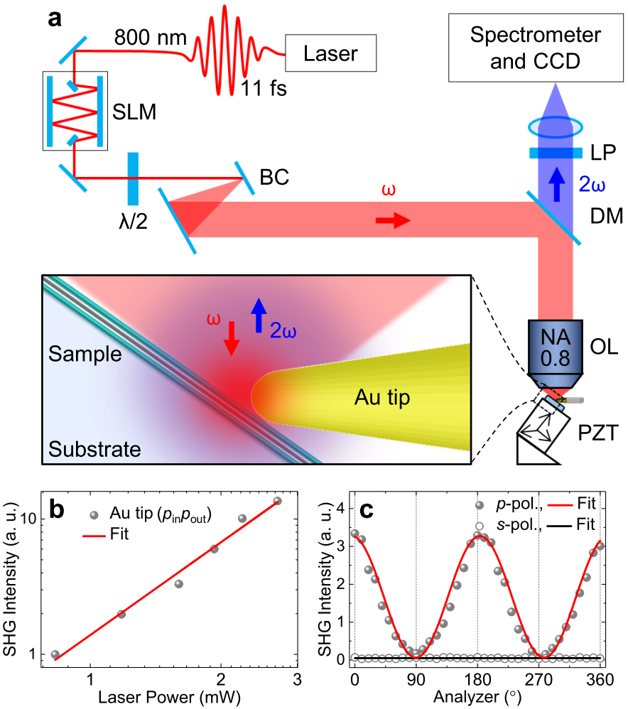
The experiment is based on tip-enhanced spectroscopy park2016tmd , with side illumination of the electrochemically etched Au tip manipulated in a shear-force AFM as shown schematically in Fig. 1a. The sample surface can be tilted by variable angle with respect to the tip axis from 0∘ to 90∘. Excitation light provided from a Ti:sapphire oscillator (FemtoSource Synergy, Femtolasers Inc., with 11 fs pulse duration, center wavelength of 800 nm, 78 MHz repetition rate, and 2 mW power) is focused onto the tip-sample junction using an objective lens (NA = 0.8, W.D. = 4 mm), with polarization and dispersion control. The backscattered SHG signal is polarization selected and detected using a spectrometer (SpectraPro 500i, Princeton Instruments, f = 500 mm) with a charge-coupled device (CCD) camera (ProEM+: 1600 eXcelon3, Princeton Instruments).
In excitation and detection, we define p and s polarization as light polarized parallel and perpendicular with respect to the plane formed by k-vector and tip axis. In pinpout (p polarized excitation and p polarized detection) configuration, the broken axial symmetry gives rise to a tip-SHG response with expected power (Fig. 1b) and polarization (Fig. 1c) dependence of the SHG response. In SHG nano-imaging, the intrinsic tip-SHG response can be discriminated from the tip-sample coupled response through polarization and tip-sample distance dependent measurements.
Note that a tilted tip geometry has been used in several cases of top-illumination tip-enhanced Raman spectroscopy (TERS) stadler2010 ; chan2011 .
However, only for the purpose of ease of tip-illumination without any vector-field control.
Vector-field control with plasmonic antenna tip
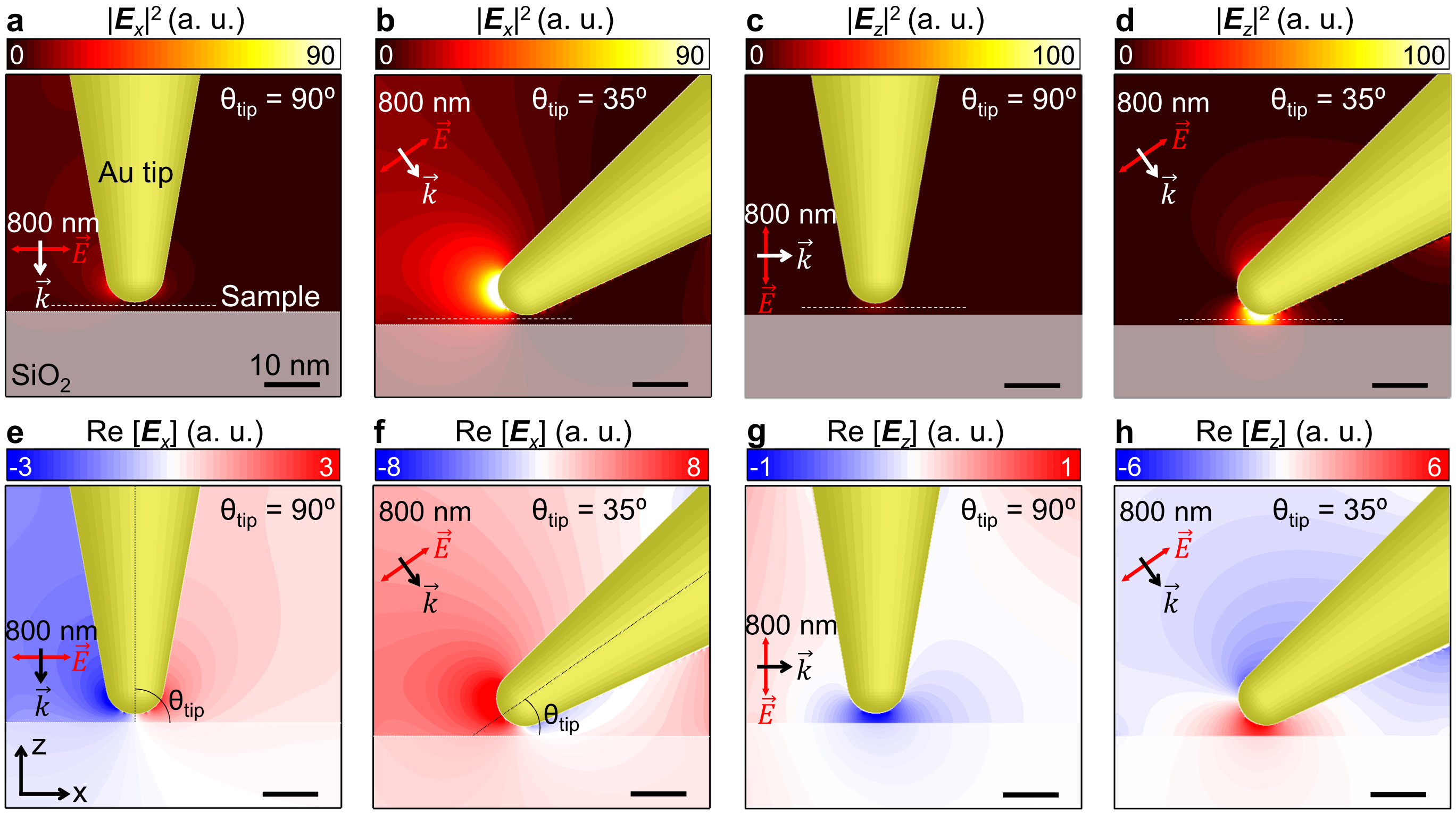
To characterize the local optical field enhancement with respect to the tilt angle of the Au tip, we calculate the expected optical field distribution using finite-difference time-domain (FDTD) simulations (Lumerical Solutions, Inc.) for our experimental conditions. Fig. 2a and e show the in-plane optical field maps ( and Re[Ex]) for surface normal tip orientation (tip = 90∘) with an SiO2 substrate, with excitation (800 nm) polarization perpendicular with respect to the tip axis. A weak Ex field confinement at the apex is seen resulting from the transverse local antenna mode talley2005 ; sanders2016 .
To achieve an efficient local plasmon antenna effect, we model the tilted tip with excitation polarization parallel with respect to the tip axis. Fig. 2b and f show calculated and Re[Ex] distributions for the 35∘ tilted tip orientation (tip = 35∘), exhibiting 6 times stronger in-plane optical field intensity enhancement compared to sample surface normal orientation (Fig. 2a). Notably, for this tilt angle, also the out-of-plane vector-field is significantly enhanced as seen in Fig. 2c-d and g-h.
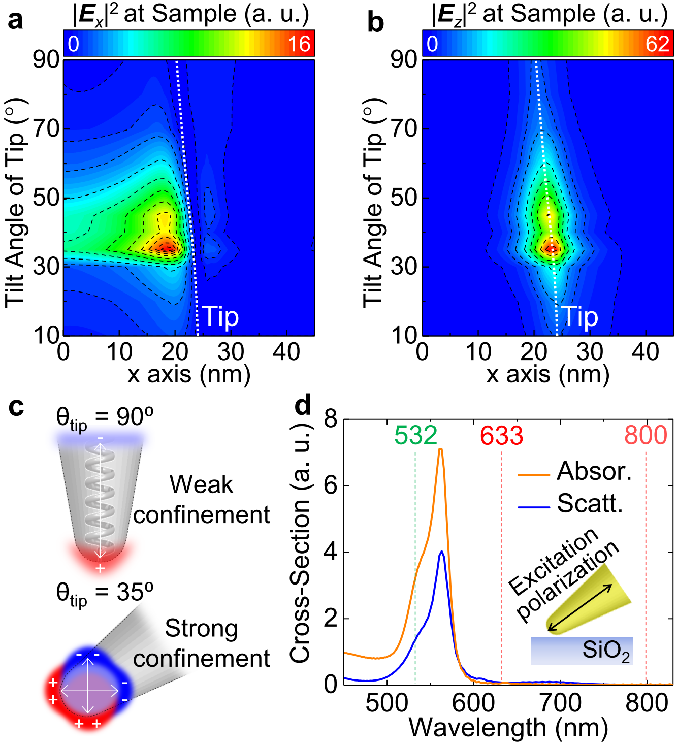
To characterize a systematic change of vector-field enhancement, we calculate the in-plane and out-of-plane optical field intensity with respect to tilt angle. Fig. 3a and b show simulated vector-field intensity profiles for and at the sample plane (the distance between tip and sample is set to 0.5 nm, see Fig. S1-S9 for full data set of the tilt angle dependent and ). For the small (10∘ tip 30∘) and large (60∘ tip 90∘) tilt angles, the field confinement is not significantly enhanced compared to conventional tip orientation (tip = 90∘) due to the overdamped resonance of the electrons oscillation in a semi-infinite tip structure. In this case, the Au tip cannot sustain antenna-like in-plane and out-of-plane surface plasmon polaritons (SPPs) sanders2016 . On the other hand, the field confinement is significantly enhanced for the tilt angles between 30∘ and 60∘ because geometrically confined free electrons give rise to an appreciable LSPR effect, as illustrated in Fig. 3c. Note that the Au tip with the SiO2 substrate provides for larger vector-field enhancement than the free standing tip because the SiO2 substrate gives rise to an induced dipole coupling between the tip and sample (see Fig. S1-S9, discussing the substrate effect) notingher2005 .
| (in-plane) | (out-of-plane) | |||
|---|---|---|---|---|
| tip = 90∘ | tip = 35∘ | tip = 90∘ | tip = 35∘ | |
| exc = 532 nm | 28 | 290 | 40 | 630 |
| exc = 633 nm | 23 | 180 | 42 | 250 |
| exc = 800 nm | 16 | 90 | 25 | 100 |
Fig. 3d shows calculated absorption and scattering cross-section spectra for the tilted Au tip (tip = 35∘) near the SiO2 substrate.
The LSPR of the tilted tip is at 550 nm near the interband transition of gold (2.4 eV), with modified spectral shape and linewidth due to the elongated structure, and correspondingly modfied radiative damping grigorchuk2012 .
Table 1 shows comparisons of the resulting in-plane and out-of-plane vector-field intensity enhancement for conventional tip (tip = 90∘) and tilted tip (tip = 35∘) for selected on and off resonance excitation wavelengths.
As can be seen, the tilted tip results in a much larger optical field enhancement for both (I/I 6-10) and (I/I 4-16) for all wavelengths, with the largest effect on resonance.
Based on these results, we understand that the tilted tip induces a strongly localized plasmon resonance to both in-plane and out-of-plane directions by creating a spatial confinement for free electrons oscillation in contrast to a reduced resonance effect for surface normal tip orientation.
Nonlinear optical nano-crystallography and nano-imaging
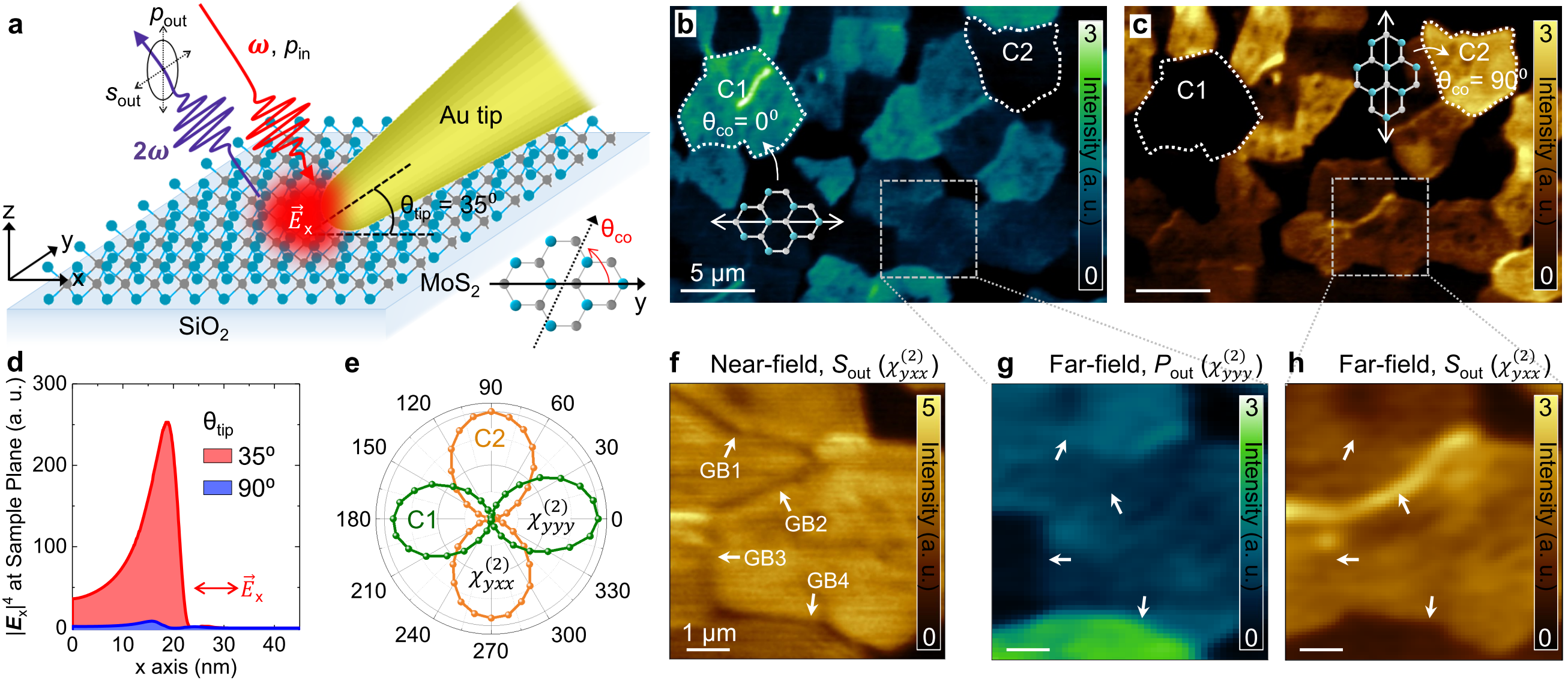
As illustrated in Fig. 4a, we perform tip-enhanced nano-SHG imaging with the 35∘ tilted antenna-tip for single-layer MoS2 films grown on a SiO2/Si substrate, as a model system of m2 point group possessing pure in-plane tensor elements malard2013 ; li2013 ; kumar2013 .
For comparison, we first perform conventional far-field imaging to determine crystal orientation angle (co) and grain boundary of the TMD crystals yin2014 ; cheng2015 . Fig. 4b and c show far-field SHG images with polarization selections of pinpout and pinsout, respectively. From the nonvanishing tensor elements and excitation condition, the induced second-order polarization for crystals with co = 0∘ (C1 of Fig. 4b-c) is given by Py(2) = 2Ey()2, where Ei=x,y,z() are the electric field components at the laser frequency (see Supporting Information for detailed matrix representations and calculations). Therefore, the SHG signal of crystals with co = 0∘ is polarized parallel to the excitation polarization (), and these crystals are clearly observed in pinpout configuration, as shown in Fig. 4b. In contrast, crystals with co = 90∘ (C2 of Fig. 4b-c) are seen most clearly in pinsout configuration (Fig. 4c) since the induced SHG polarization is given by Py(2) = -2Ex()2. This polarization dependence on crystallographic orientation is also confirmed in far-field SHG anisotropy measured with rotating analyzer (Fig. 4e).
Only Ex() contributes to the SHG signal in pinsout configuration. Therefore, with I2ω P(2)2 E()4, we can calculate the enhanced SHG intensity using the 35∘ tilted tip (I) compared to the conventional surface normal oriented tip (I) from the FDTD simulation. As shown in Fig. 4d, the spatially integrated Ex()4 for the 35∘ tilted tip at the sample plane is 28 times larger than that of the surface normal oriented tip (tip = 90∘), i.e., I/I 28.
Fig. 4f shows a measured tip-enhanced nano-SHG image in pinsout configuration for a small area selected within the far-field image. Far-field images of pout and sout detection are magnified in Fig. 4g and h for comparison. As demonstrated previously yin2014 ; cheng2015 , some GBs are visualized in the far-field SHG images due to the constructive (or destructive) interference between SHG signals of adjacent crystals. However, this interference contrast at GBs is observed only for specific crystal orientation or polarization condition cheng2015 .
In contrast, in the tip-enhanced SHG image (Fig. 4f), a full GB map is obtained with pronounced SHG contrast. For example, while GB2 is observed in both far- and near-field images, the additional GBs (GB1, GB3, and GB4) are only seen in the near-field image. In contrast to the far-field response, a full GB map can be obtained regardless of crystal orientation and interference.
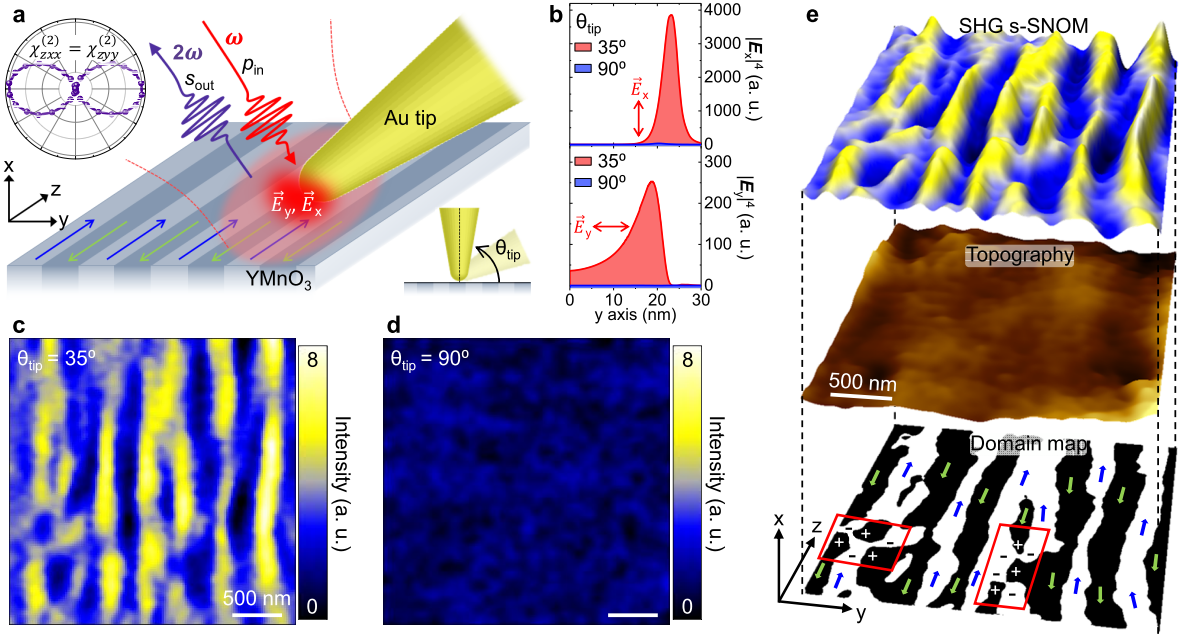
In order to assess the full benefit of increased both in- and out-of-plane field confinement (Fig. 2d), we then perform tip-enhanced nano-SHG imaging on single-crystalline x-cut YMnO3, as a model system of 6mm point group with both in-plane and out-of-plane nonlinear optical susceptibility fiebig2002 ; neacsu2009 . We first deduce the microscopic sample orientation from far-field SHG anisotropy measurement, as shown in Fig. 5a. Based on this information, we probe the ferroelectric = tensor elements in pinsout tip-enhanced near-field microscopy configuration. The corresponding SHG polarization is then given by Pz(2) = 2(Ex()2+Ey()2) (see Supporting Information for detailed matrix representations and calculations). The measured intensity I2ω is proportional to Ex()2+Ey()22 = Ex()4 + Ey()4 + 2Ex()2Ey()2. From the spatially integrated Ex()4, Ey()4, Ex()2, and Ey()2 values at the sample plane for the 35∘ tilted and surface normal oriented tips (Fig. 5b), we can estimate the tip-enhanced SHG intensity ratio of I/I 27.
Fig. 5c and d show the resulting tip-enhanced SHG images under tilted tip (tip = 35∘) and surface normal tip (tip = 90∘) configuration. We observe a high contrast image of the domains only with the tilted tip. The details of contrast are due to the interference between the tip-enhanced SHG from a single domain and residual far-field SHG from multiple domains giving rise to a local phase-sensitive signal neacsu2009 . From that image, we can obtain the corresponding ferroelectric domain map exhibiting an alternating ferroelectric polarization pattern as expected for this crystallographic orientation (Fig. 5e). In addition, we observe the 3-fold symmetric vortices of the domains (red boxes) as expected for hexagonal manganites chae2012 ; jungk2010 which provides information for the understanding of topological behaviors of ferroics.
In summary, a conventional surface normal oriented tip geometry in tip-enhanced near-field microscopy gives limited polarization control in both the intrinsic far-field excitation and the extrinsic near-field nano-optical response.
Furthermore, for surface normal tip orientation, the antenna mode driven into a semi-infinite tip structure results in reduced field enhancement due to overdamping, which gives rise to reduced efficiency for both in-plane and out-of-plane nano-optical response.
Our work presents a simple but powerful solution to control the vector-field of a nano-optical antenna-tip.
We show that the optical field confinement can be systematically controlled by tuning the tip orientation angle with respect to the sample surface, to enhance the in-plane optical field (Ex) confinement for investigation of 2D materials.
Surprisingly, rather than an associated decrease in out-of-plane sensitivity with increasing tilt angle, the out-of-plane optical field (Ez) is also enhanced with an even larger enhancement factor than Ex.
We find that at an optimized angle near 35∘ with details depending on tip material, sample, and excitation wavelength, the broken axial symmetry provides for a more sensitive nano-probe beyond conventional near-field microscopy tip for all optical modalities and any sample.
The vector-field controllability of plasmonic antenna-tip not only allows probing selective polarization components of samples by simply changing its tilting angle but also this strongly confined vector-field gives access to anomalous nanoscale light-matter interactions such as exciton-plasmon coupling park2017dark , electron-phonon coupling jin2016 , and strong coupling chikkaraddy2016 in a range of photoactive molecules and quantum materials.
References
- (1) Anastassakis, E. Selection rules of raman scattering by optical phonons in strained cubic crystals. J. Appl. Phys. 82, 1582–1591 (1997).
- (2) Fiebig, M. et al. Determination of the magnetic symmetry of hexagonal manganites by second harmonic generation. Phys. Rev. Lett. 84, 5620 (2000).
- (3) Najafov, H. et al. Observation of long-range exciton diffusion in highly ordered organic semiconductors. Nat. Mater. 9, 938 (2010).
- (4) Yin, X. et al. Edge nonlinear optics on a MoS2 atomic monolayer. Science 344, 488–490 (2014).
- (5) Gerton, J. M., Wade, L. A., Lessard, G. A., Ma, Z. & Quake, S. R. Tip-enhanced fluorescence microscopy at 10 nanometer resolution. Phys. Rev. Lett. 93, 180801 (2004).
- (6) Yano, T.-a., Verma, P., Saito, Y., Ichimura, T. & Kawata, S. Pressure-assisted tip-enhanced raman imaging at a resolution of a few nanometres. Nat. Photon. 3, 473–477 (2009).
- (7) Zhang, R. et al. Chemical mapping of a single molecule by plasmon-enhanced raman scattering. Nature 498, 82–86 (2013).
- (8) Lee, K. et al. Vector field microscopic imaging of light. Nat. Photon. 1, 53–56 (2007).
- (9) Olmon, R. L. et al. Determination of electric-field, magnetic-field, and electric-current distributions of infrared optical antennas: a near-field optical vector network analyzer. Phys. Rev. Lett. 105, 167403 (2010).
- (10) Burresi, M. et al. Probing the magnetic field of light at optical frequencies. Science 326, 550–553 (2009).
- (11) Kihm, H. et al. Bethe-hole polarization analyser for the magnetic vector of light. Nat. Commun. 2, 451 (2011).
- (12) Gerber, J. A., Berweger, S., O’Callahan, B. T. & Raschke, M. B. Phase-resolved surface plasmon interferometry of graphene. Phys. Rev. Lett. 113, 055502 (2014).
- (13) Fei, Z. et al. Gate-tuning of graphene plasmons revealed by infrared nano-imaging. Nature 487, 82 (2012).
- (14) Chen, J. et al. Optical nano-imaging of gate-tunable graphene plasmons. Nature 487, 77–81 (2012).
- (15) Park, K.-D. et al. Hybrid tip-enhanced nanospectroscopy and nanoimaging of monolayer WSe2 with local strain control. Nano Lett. 16, 2621–2627 (2016).
- (16) Bao, W. et al. Visualizing nanoscale excitonic relaxation properties of disordered edges and grain boundaries in monolayer molybdenum disulfide. Nat. Commun. 6, 8993 (2015).
- (17) Li, Z. et al. Active light control of the MoS2 monolayer exciton binding energy. ACS Nano 9, 10158–10164 (2015).
- (18) Damodaran, A. et al. Phase coexistence and electric-field control of toroidal order in oxide superlattices. Nat. Mater. (2017).
- (19) Kalantar-zadeh, K. et al. Two dimensional and layered transition metal oxides. Appl. Mater. Today 5, 73–89 (2016).
- (20) Kildishev, A. V., Boltasseva, A. & Shalaev, V. M. Planar photonics with metasurfaces. Science 339, 1232009 (2013).
- (21) Berweger, S. et al. Optical nanocrystallography with tip-enhanced phonon raman spectroscopy. Nat. Nanotech. 4, 496–499 (2009).
- (22) Muller, E. A., Pollard, B., Bechtel, H. A., van Blerkom, P. & Raschke, M. B. Infrared vibrational nanocrystallography and nanoimaging. Sci. Adv. 2, e1601006 (2016).
- (23) Talley, C. E. et al. Surface-enhanced raman scattering from individual Au nanoparticles and nanoparticle dimer substrates. Nano Lett. 5, 1569–1574 (2005).
- (24) Sanders, A. et al. Understanding the plasmonics of nanostructured atomic force microscopy tips. Appl. Phys. Lett. 109, 153110 (2016).
- (25) Kumar, N. et al. Second harmonic microscopy of monolayer MoS2. Phys. Rev. B 87, 161403 (2013).
- (26) Seyler, K. L. et al. Electrical control of second-harmonic generation in a WSe2 monolayer transistor. Nat. Nanotech. 10, 407–411 (2015).
- (27) Hsu, W.-T. et al. Second harmonic generation from artificially stacked transition metal dichalcogenide twisted bilayers. ACS Nano 8, 2951–2958 (2014).
- (28) Fiebig, M., Fröhlich, D., Lottermoser, T. & Maat, M. Probing of ferroelectric surface and bulk domains in RMnO3 (R = Y, Ho) by second harmonic generation. Phys. Rev. B 66, 144102 (2002).
- (29) Neacsu, C. C., van Aken, B. B., Fiebig, M. & Raschke, M. B. Second-harmonic near-field imaging of ferroelectric domain structure of YMnO3. Phys. Rev. B 79, 100107 (2009).
- (30) Stadler, J., Schmid, T. & Zenobi, R. Nanoscale chemical imaging using top-illumination tip-enhanced raman spectroscopy. Nano Lett. 10, 4514–4520 (2010).
- (31) Chan, K. A. & Kazarian, S. G. Tip-enhanced raman mapping with top-illumination afm. Nanotechnology 22, 175701 (2011).
- (32) Notingher, I. & Elfick, A. Effect of sample and substrate electric properties on the electric field enhancement at the apex of spm nanotips. J. Phys. Chem. B 109, 15699–15706 (2005).
- (33) Grigorchuk, N. I. Radiative damping of surface plasmon resonance in spheroidal metallic nanoparticle embedded in a dielectric medium. JOSA B 29, 3404–3411 (2012).
- (34) Malard, L. M., Alencar, T. V., Barboza, A. P. M., Mak, K. F. & de Paula, A. M. Observation of intense second harmonic generation from MoS2 atomic crystals. Phys. Rev. B 87, 201401 (2013).
- (35) Li, Y. et al. Probing symmetry properties of few-layer MoS2 and h-BN by optical second-harmonic generation. Nano Lett. 13, 3329–3333 (2013).
- (36) Cheng, J. et al. Kinetic nature of grain boundary formation in as-grown MoS2 monolayers. Adv. Mater. 27, 4069–4074 (2015).
- (37) Chae, S. et al. Direct observation of the proliferation of ferroelectric loop domains and vortex-antivortex pairs. Phys. Rev. Lett. 108, 167603 (2012).
- (38) Jungk, T., Hoffmann, Á., Fiebig, M. & Soergel, E. Electrostatic topology of ferroelectric domains in YMnO3. Appl. Phys. Lett. 97, 012904 (2010).
- (39) Park, K.-D., Jiang, T., Clark, G., Xu, X. & Raschke, M. B. Radiative control of dark excitons at room temperature by nano-optical antenna-tip induced Purcell effect. preprint arXiv:1706.09085, Nat. Nanotech. (2017).
- (40) Jin, C. et al. Interlayer electron-phonon coupling in WSe2/hBN heterostructures. Nat. Phys. 13, 127–131 (2017).
- (41) Chikkaraddy, R. et al. Single-molecule strong coupling at room temperature in plasmonic nanocavities. Nature 535, 127–130 (2016).
Acknowledgements
The authors would like to thank Joanna M. Atkin for insightful discussions.
We thank Xiaobo Yin and Manfred Fiebig for providing the MoS2 sample and the YMnO3 sample, respectively.
We acknowledge funding from the U.S. Department of Energy, Office of Basic Sciences, Division of Material Sciences and Engineering, under Award No. DE-SC0008807.
We also acknowledge support provided by the Center for Experiments on Quantum Materials (CEQM) of the University of Colorado.
Competing financial interests
The authors declare no competing financial interests.