Metal-insulator transition in CaVO3 thin films: interplay between epitaxial strain, dimensional confinement, and surface effects
Abstract
We use density functional theory plus dynamical mean-field theory (DFT+DMFT) to study multiple control parameters for tuning the metal-insulator transition (MIT) in CaVO3 thin films. We focus on separating the effects resulting from substrate-induced epitaxial strain from those related to the reduced thickness of the film. We show that tensile epitaxial strain of around 3-4% is sufficient to induce a transition to a paramagnetic Mott-insulating phase. This corresponds to the level of strain that could be achieved on a SrTiO3 substrate. Using free-standing slab models, we then demonstrate that reduced film thickness can also cause a MIT in CaVO3, however, only for thicknesses of less than 4 perovskite units. Our calculations indicate that the MIT in such ultra-thin films results mainly from a surface-induced crystal-field splitting between the -orbitals, favoring the formation of an orbitally-polarized Mott insulator. This surface-induced crystal-field splitting is of the same type as the one resulting from tensile epitaxial strain, and thus the two effects can also cooperate. Furthermore, our calculations confirm an enhancement of correlation effects at the film surface, resulting in a reduced quasiparticle spectral weight in the outermost layer, whereas bulk-like properties are recovered within only a few layers away from the surface.
I Introduction
Transition-metal oxides offer an interesting playground, of both technological and fundamental importance, which allows to engineer materials properties through the fine-tuning of both structure and stoichiometry [1; 2]. Electronic, magnetic, and structural properties of these materials are often strongly coupled, due to the localized nature of the electrons of the transition metal cation, which form narrow bands around the Fermi level dominating the electronic properties. This can lead to a number of exotic phenomena such as metal-insulator transitions (MITs), colossal magneto-resistance, or high-temperature superconductivity [3].
Progress in modern thin film growth techniques has opened up additional possibilities for tuning materials properties by growing oxide heterostructures, such as superlattices or thin films, with essentially atomically sharp interfaces [4]. The physical properties of such heterostructures can be tuned by choosing the appropriate combination of constituents, as well as the super-periodicity or the film thickness. Furthermore, within the interfacial region of these heterostructures, completely novel properties can emerge, that are usually not found in the corresponding bulk constituents [5]. A striking example for such an emerging interfacial property is the high-mobility two-dimensional electron gas observed at the interface of the two insulators LaAlO3 and SrTiO3 [6].
In fact, such dramatic changes of the conductive properties compared to the corresponding bulk materials are not necessarily restricted to the interfacial region. Examples are the MITs observed in thin films of various transition metal oxides, including, e.g., vanadates [7; 8; 9], titanates [10; 11], manganates [12], nickelates [13; 14; 15; 16], or iridates [17]. Several of these materials are metallic in their bulk forms (e.g., SrVO3, CaVO3, La2/3Ca1/3MnO3, LaNiO3, or SrIrO3) and become insulating when the film thickness is reduced below a certain critical value. The source for this MIT is often ascribed to confinement effects, which restrict electron movement to the in-plane directions of the film and lead to the formation of quantum well states [18; 19]. However, the reported critical thicknesses for different materials are rather wide-spread, e.g., 3 respectively 5 unit cells for La2/3Ca1/3MnO3 [12] and LaNiO3 [14], compared to 4 nm ( unit cells) in CaVO3 [9]. Furthermore, even for different samples of the same material, the reported critical thicknesses can differ quite significantly, e.g., 2-3 unit cells for SrVO3 in Ref. 7, compared to 6.5 nm ( unit cells) in Ref. 8. This indicates that factors other than dimensional confinement need to be taken into account to fully understand the origin of such thickness-dependent MITs.
For example, it has been suggested, based on first-principles electronic structure calculations, that early transition metal perovskites such as SrVO3 and CaVO3 can become insulating under strong tensile epitaxial strain [20]. Such epitaxial strain is often present in thin film samples due to the lattice mismatch between the thin film and substrate materials. It has also been reported that the critical thickness for the MIT in La2/3Sr1/3MnO3 is increased by the presence of both strain and oxygen vacancies [12], and that a transition from metallic to insulating behavior can be induced in SrIrO3 both by reducing the film thickness or by applying compressive strain through a suitably chosen substrate [17]. The opposite effect, i.e., a transition from a bulk Mott insulator to a metallic thin film, has been reported for LaTiO3 [10; 11], and attributed to the effect of compressive epitaxial strain [21]. Similarly, it has been found that the transition to the low temperature insulating state in bulk NdNiO3 and SmNiO3 can be completely suppressed by epitaxial strain [13; 15], and a competition of strain (in this case favoring the metallic state) and dimensionality effects (favoring the insulating state) has been reported for NdNiO3 [16].
Here, we focus on the case of CaVO3, which in its bulk form exhibits relatively high resistivities [22]. Furthermore, its spectral properties point towards a strongly correlated metal [23; 24], making it an ideal candidate to probe the sensitivity of the Mott MIT to strain and dimensionality effects. Indeed, as already mentioned above, recent experiments have reported a dramatic thickness-dependent change in the conducting properties of CaVO3 films grown on SrTiO3 [9]. The sheet resistance at low temperatures was shown to increase by orders of magnitude with decreasing film thickness, and the temperature dependence of the resistivity changed from metallic, for films thicker than 4 nm, to insulating, for the thinnest films.
In Ref. 9, the thickness-dependent MIT has been attributed to a reduction of the effective bandwidth, resulting from a dimensional crossover from 3D to 2D. However, an alternative scenario for the observed MIT, related to a thickness-dependent relaxation of epitaxial strain, is outlined in the following. In principle, large tensile epitaxial strain could be achieved in CaVO3 films grown on a SrTiO3 substrate, with a nominal lattice mismatch of 3.5 %. However, the out-of-plane lattice parameters measured in an earlier study by Liberati et al. [25] indicate that for such a large mismatch, the films tend to relax (at least partially) back toward the bulk CaVO3 lattice parameters. Strain relaxation has also been confirmed for a 53 nm thick film investigated in Ref. 9. However, the strain states of the thinner films have not been characterized. Typically, fully strained epitaxial films can be grown up to a materials- and strain-dependent critical thickness, above which the energy cost for forming misfit dislocations becomes less than the elastic energy of a coherently strained film [26]. It is thus possible, that in very thin films, CaVO3 is essentially fully strained to the in-plane lattice constant of the SrTiO3 substrate. Such strong tensile strain can induce a transition to insulating behavior, as predicted in Ref. 20. For increasing film thickness, the epitaxial strain is then successively released, recovering the bulk-like metallic behavior in thicker films. We note that for the rather large lattice mismatch between CaVO3 and SrTiO3, the critical thickness for the formation of misfit dislocations could be rather small.
In this article, we assess the likelihood of this scenario, using first principles-based electronic structure calculations. In particular, we clarify the roles of both strain and reduced dimensionality on the MIT in CaVO3 and related materials by first incorporating each effect individually before treating them together within our calculations. For a realistic description of the MIT, we use a combination of density functional theory and dynamical mean-field theory (DFT+DMFT) [27; 28; 29; 30], which allows to obtain the Mott-insulating state without the need to artifically introduce a symmetry-broken state with magnetic and/or orbital long range order. In addition, the DFT+DMFT method accounts well for correlation effects within the metallic state, as demonstrated, e.g., for bulk CaVO3 and the related SrVO3 [31; 23].
The remainder of this article is organized as follows. After describing our computational method in Sec. II, we first confirm the prediction of Ref. 20, and show that tensile strain slightly above 3% is sufficient to induce a MIT in CaVO3 (Sec. III). We isolate the individual effect of tensile epitaxial strain by using bulk unit cells with constrained “in-plane” cell parameters, thereby mimicking the elastic constraint present in epitaxial films. Then, in Sec. IV, we explore finite size effects within strain-free slab geometries, i.e., corresponding to free-standing ultra-thin films with thicknesses of 2-6 perovskite units. Indeed, we find the thinnest slabs to be insulating. However, the metallicity is recovered already for a thickness of 4 perovskite units, i.e., corresponding to film thicknesses of about 1.5 nm. The Mott-insulating character of the ultra-thin slabs can be traced back to a surface-induced crystal-field splitting, similar to what has been suggested recently from DFT+DMFT calculations for 2 unit cells of SrVO3 sandwiched between vacuum and a SrTiO3 “substrate” [32]. The surface-induced crystal-field splitting also leads to enhanced correlation effects in the surface layer of the thicker CaVO3 slabs, indicated, e.g., by a large quasiparticle mass enhancement. This is in good agreement with experimental photoemission results [33; 34] and previous DMFT-based studies for SrVO3 [35]. Finally, we show that strain and finite-size effects cooperate, but that the strain effect is clearly dominating, at least for thicknesses above 4 perovskite units. This suggests that the scenario described above, i.e., successive strain relaxation with increasing film thickness as main mechanism behind the observed thickness-dependent MIT in CaVO3, is indeed highly plausible. Further experimental characterization is required to verify this scenario. Our work shows that it is crucial to take into account the interplay of a variety of factors, such as, e.g., epitaxial strain, dimensional confinement, defects, as well as genuine interface or surface effects, in order to fully understand the emerging properties observed in complex oxide heterostructures.
II Computational Method
We use the Quantum ESPRESSO package [36] together with the PBE functional [37] to calculate the electronic structure within DFT and perform all structural relaxations. To address the effect of epitaxial strain, we use the bulk unit cell of CaVO3 and constrain the orthorhombic “in-plane” lattice constants and to be equal to a given , while relaxing the “out-of-plane” lattice parameter and all internal structural degrees of freedom (atomic positions). Thus, we use a geometry where the long orthorhombic axis is perpendicular to the plane defined by the substrate surface, which preserves the orthorhombic symmetry (c.f. Ref. 38). The epitaxial strain is then defined as , where is the in-plane lattice constant corresponding to the unstrained system, which we choose as the average of and in the fully relaxed bulk system.
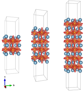
To address the finite size effect, we use slab supercells consisting of 2 perovskite units, , stacked along the direction and terminated by CaO layers on both sides, which are separated by a sufficient amount of vacuum, as shown in Fig. 1. The slabs are built starting from the bulk structure and thus employ lattice vectors (relative to the simple perovskite unit) perpendicular to , such as to allow for the same octahedral tilt pattern as in the bulk structure. This slab geometry preserves the mirror plane perpendicular to within the central CaO layer of the slab, as well as the glide plane parallel to , while the glide plane is not preserved (since has its glide vector perpendicular to which is not the case for ). Thus, the upper and lower halfs of the slabs are symmetry-equivalent due to , and the two V sites within each layer are symmetry-equivalent due to , resulting in only inequivalent V sites per slab. We use the same lattice constant along both in-plane directions of the slab, analogous to the unstrained bulk reference state. In order to assess the combined effect of strain and finite size, we also perform calculations for “epitaxially strained” slabs, where we constrain the in-plane lattice constant to values larger than . During the structural relaxation of the slabs, the atomic positions within the two inner layers are fixed to the corresponding bulk structures (at the given strain), while all other positions (present only for ) are relaxed. Even for , the outermost CaO layer is also relaxed. We found that a vacuum layer of 16 Å is necessary and sufficient to avoid cross-talk between the periodic images along .
We use standard PBE scalar-relativistic ultrasoft pseudopotentials from the Quantum ESPRESSO website, where the and semicore states of both Ca and V are treated as valence electrons. The plane-wave energy cutoffs for the expansion of wave-functions and charge density are set to 40 and 300 Ry, respectively. Brillouin zone integrals are evaluated using the Methfessel-Paxton method with a smearing parameter of 0.02 Ry and a -point grid for the unit cell of CaVO3, which is reduced to a grid for all slab unit cells.
After relaxing the structure within PBE-DFT, we construct maximally localized Wannier functions (MLWFs) [39] for the -derived bands around the Fermi level, using the wannier90 code [40]. We obtain three V-centered -like MLWFs per V atom, which we use as basis orbitals to describe the low-energy correlated subspace of CaVO3 (c.f. Ref. 41). The electron-electron interaction within this correlated subspace is then treated within DMFT to obtain local Green’s functions.
The DMFT calculations are implemented using the TRIQS/DFTTools libraries [42; 43]. In the DMFT calculations for the slab unit cells, a separate impurity problem is solved for each of the inequivalent V sites (one for each layer ), using the TRIQS/CTHYB solver [44; 45]. The different impurity problems are then connected through the self-consistency condition for the lattice Green’s function. We use the Slater-Kanamori form, including spin-flip and pair-hopping terms, to describe the local Coulomb interaction between the electrons on the impurity sites, and we include all off-diagonal elements of the local Green’s function and self-energy in the calculation (after transforming to a coordinate system where the local MLWF Hamiltonian is diagonal). All DMFT calculations are performed for an inverse electronic temperature of , which corresponds to approximately room temperature. From the imaginary-time Green’s function, , we obtain the orbital occupations, , and the “averaged” spectral density at the Fermi level, , which approaches for decreasing temperature, i.e., in the limit (c.f. [46]). The full real-frequency spectral functions, , are obtained from using the maximum entropy method [47].
III Effect of epitaxial strain
| DFT | 5.319 | 5.365 | 7.554 | 3.777 | 7.9 | 9.4 |
| Exp. | 5.322 | 5.343 | 7.547 | 3.771 | 7.9 | 9.3 |
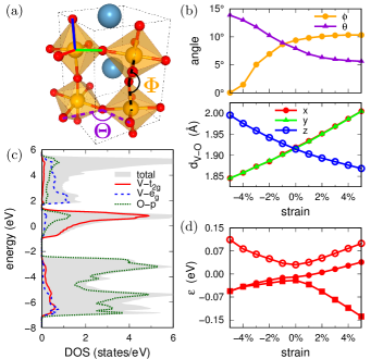
We first relax the bulk structure (cell parameters as well as atomic positions) without applying any constraints within DFT. To characterize the V–O–V bond angles in the relaxed structures, we use the conventional rotation and tilt angles, and , corresponding to the tilt system (see Fig. 2a and, e.g., Ref. [48]). As seen from Table 1, these angles as well as the relaxed lattice parameters are in excellent agreement with experimental data obtained from neutron diffraction [22].
.
We then study the effect of epitaxial strain on the crystal structure of CaVO3 for the case of a square-lattice substrate (e.g., SrTiO3) by constraining the in-plane cell parameters while relaxing all other structural degrees of freedom, as explained in Sec. II. The theoretical bulk structure has a ratio of , slightly different from 1, so we choose to refer the nominal strain value to the average in-plane spacing .
The application of strain strongly influences the internal degrees of freedom of the crystal structure, especially bond angles and bond distances. The variation of the two conventional rotation and tilt angles, as well as of the V–O bond lengths, are shown in Fig. 2b as function of strain. Under compressive strain, the out-of-plane bonds show a strong tendency to straighten, leading to a complete suppression of tilts for compressive strains stronger than 4 %. Simultaneously, the rotation angle increases significantly with respect to the unstrained case. Under tensile strain, the opposite trend is observed, i.e., increasing out-of-plane tilts and decreasing in-plane rotations. However both angles tend to saturate towards large tensile strain, to values of around and , respectively, i.e., only slightly larger, respectively smaller, than the bulk values. Regarding the V–O bond lengths, we note that the in-plane V–O bond lengths follow the applied strain, while the out-of-plane bond length exhibits the opposite trend, dictated by the expansion (contraction) of the out-of plane cell parameters in response to compressive (tensile) strain. These trends are similar to what has been reported for other early transition metal perovskite oxides (see, e.g., Refs. [21; 38]).
The electronic density of states (both total and projected on atomic V-/ and O- orbitals) for unstrained CaVO3 is shown in Fig. 2c. It can be seen, that a metallic state is obtained within DFT, and that the electronic states around the Fermi level are formed by a group of bands with dominant V- character, which is separated from other bands at higher and lower energies. The densities of states for the strained structures are qualitatively similar to that. For each of these structures, we now construct MLWFs corresponding to the V--dominated bands around the Fermi energy. As for other early transition metal oxides (see, e.g., Refs. [29; 21]), we obtain three MLWFs per V site, which resemble atomic orbitals, albeit with strong -like tails on the surrounding oxygen ligands.
We then calculate the matrix elements of the Kohn-Sham Hamiltonian, , where are the orbital indeces of the MLWFs and R and indicate different V sites 111We note that here we are using a simplified notation where R and R’ do not necessarily correspond to lattice translations of the structure. Thus, strictly speaking, these matrix elements can depend on both R and . However, since all V sites are equivalent, one can always find a local transformation such that the matrix elements for different R become identical.. Thereby, orbital “3” generally resembles , i.e., it is almost in-plane, while orbitals “1” and “2” resemble linear combinations of and . The crystal-field levels , obtained as eigenvalues of the on-site matrix , are shown as function of strain in Fig. 2d. They exhibit the same trends that have already been observed in similar systems [20]. The epitaxial stain induces a tetragonal-like splitting between the three -MLWFs that depends approximately linear on the strain, with one orbital at higher and two orbitals at lower energies under strong compressive strain, and vice versa under strong tensile strain. Superimposed on this tetragonal-like splitting is the effect of the octahedral tilts and rotations, which lifts the degeneracy between the three orbitals already for zero strain, and also splits the two higher lying levels in the tensile strain regime. Under compressive strain, this additonal splitting is small and vanishes completely below % strain, due to the suppression of the out-of-plane tilts which raises the symmetry of the system to tetragonal. Further, we note that the nearest neighbor hopping amplitudes exhibit a similar strain dependence to what has been reported previously for related systems [20].
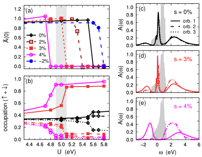
Next, we investigate whether epitaxial strain facilitates the formation of a Mott-insulating state in CaVO3, by performing DMFT calculations within the correlated subspace defined in the MLWF basis, as described in Sec. II. Fig. 3a shows , the averaged spectral weight around the Fermi level, as function of the interaction parameter for different values of strain. For the unstrained case (black line) one observes a MIT at , i.e., the system is metallic () for and insulating () for larger values. Thus, for a typical value of , which has been used previously for CaVO3 and related materials [31], the system is metallic but not too far from the MIT, confirming the nature of unstrained CaVO3 as “correlated metal”.
Considering now the results for the strained systems, one observes that epitaxial strain has a remarkable effect on the electronic properties of CaVO3. Under tensile strain, the critical value of at which the MIT occurs is strongly shifted to lower values, reaching the region around for strains between 3 % and 4 %. In contrast, the critical for the MIT is increased under compressive strain. These trends are in line with the general considerations discussed in Ref. [20]. Fig. 3c-e show the spectral functions calculated for . One can see that a sizable gap of opens in the bands for a strain of about 4 % (Fig. 3e), while already at 3 % strain (Fig. 3d) there is a narrowing of the quasiparticle peak compared to the unstrained case. These spectral changes are accompanied by noticeable changes in the orbital occupations, as shown in Fig. 3b. In the unstrained case, all three -orbitals are equally occupied in the metallic regime, and only a weak orbital polarization develops in the insulating state, i.e. for high values of . In contrast, under 3 % and 4 % tensile strain, there is a sizeable orbital polarization already in the metallic state, and the system becomes essentially fully polarized, with one half-filled and two empty orbitals, in the insulating regime. This is consistent with the strain-induced crystal-field splitting shown in Fig. 2d, and is analogous to what has been reported for other perovskites in Refs. 20 and 21.
It follows that the level of strain achievable in CaVO3 thin films using SrTiO3 as substrate (about 3.5% tensile strain) is expected to bring the system right at the boundary of a MIT (or even across it).
IV Effect of dimensional confinement
Next, we investigate how confinement perpendicular to the substrate plane, due to finite film thickness, affects the tendency of CaVO3 to undergo a MIT. For this, we consider unstrained free-standing slab unit cells of CaVO3, with thicknesses varying from 2 to 6 simple perovskite unit cells (corresponding to about 0.8 nm to 2.2 nm), as described in Sec. II and also shown in Fig. 1. We note that, while here we are using the free-standing slab geometry mainly as model systems to isolate finite size effects from other factors affecting the MIT, a procedure to experimentally fabricate such free-standing perovskite films has in fact been recently reported [50].
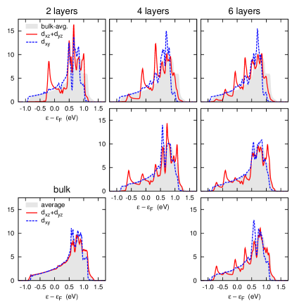
After structural relaxation of the different slabs, as described in Sec. II, we construct MLWFs for the V--dominated bands around the Fermi level. Similar to the corresponding bulk system (shown in Fig. 2c), these bands are well separated from other bands at higher and lower energies, and the resulting MLWFs are centered on the V sites with strong local character plus additional O- contributions on the surrounding ligands. Fig. 4 shows the layer- and orbitally-resolved (in the MLWF basis) densities of states (DOS) of these “-bands” for the three different slabs with different thicknesses. For comparison, also the corresponding DOS for the (unstrained) bulk system is shown.
One can see that, in the dimensionally-confined systems, there is a clear difference between the DOS corresponding to the in-plane -like MLWFs and the one corresponding to the other two orbitals, whereas in the bulk case the DOS of all three MLWFs are very similar. Due to its orientation within the - plane and the nearly two-dimensional character of the corresponding band, the -orbital is not very sensitive to the confinement along and exhibits a similar bandwidth as in the bulk. In contrast, the other two orbitals have a significantly reduced bandwidth in the 1-bilayer slab, but also (to a minor extent) in the 2- and 3-bilayer slabs. In all cases, the corresponding DOS exhibits an evident subband structure, manifested as multiple peaks, due to the confinement along the direction. The quantum well states responsible for this subband structure are spread throughout the slab, as can be seen from the matching peaks in the DOS corresponding to different layers. This was described in more detail for SrVO3 slabs by Zhong et al. [19].
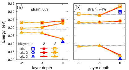
We now examine the changes of the crystal-field levels for the different slabs. In Fig. 5a, the crystal-field splitting between the -orbitals is shown as a function of the layer depth for the 1-, 2-, and 3-bilayer slabs (), together with the bulk values as reference. It can be seen, that the results for are nearly indistinguishable from the two outer layers of the 3-bilayer slab, and that the crystal-field levels in the inner layer of the slab are already very similar to the bulk reference. This shows that the influence of the surface decays very rapidly towards the inside of the material and is nearly restricted to only the outermost layer. Furthermore, a strong crystal-field splitting is apparent in the surface layer for all slab thicknesses. The -dominated orbital is lowered in energy with respect to the other two orbitals, which in turn become almost degenerate. This is similar to what has been reported in Ref. 32 for ultra-thin SrVO3, and follows from the tetragonal-like symmetry-breaking at the surface. The splitting between and / is largest in the 1-bilayer (which consists only of two surface layers) and converges to about 110 meV already for . The magnitude of this splitting is comparable to the crystal-field splitting induced by a tensile strain of about 3% in the bulk system, and thus can be expected to have a noticeable effect on the MIT.
We note that, in contrast to the local crystal-field energies, the nearest neighbor hopping amplitudes (not shown) are only weakly affected by the presence of the surface, and are overall very similar to the bulk case (except, of course, that there is no hopping into the vacuum layer).
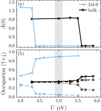
We now perform DMFT calculations for the different slabs, using the low-energy correlated subspace defined by the -MLWFs. We first discuss the results for the 1-bilayer slab. From the evolution of , shown as function of the interaction strength in Fig. 6a, it can be seen that there is a large shift of the critical value for the MIT, , from 5.6 eV in the unstrained bulk case to 4.4 eV in the 1-bilayer slab. Furthermore, from the corresponding orbital occupations shown in Fig. 6b, one can see that the 1-bilayer slab is essentially fully orbitally polarized in the Mott-insulating state, with one half-filled and two empty orbitals, consistent with the strong crystal-field splitting discussed above. Considering a realistic value for the bulk system of around 5 eV (see Sec. III), and taking into account that the value for the ultrathin slab is likely to be even somewhat larger due to reduced screening, our results indicate that 1-bilayer of CaVO3 is insulating, analogous to 1-bilayer of SrVO3 [7; 32].
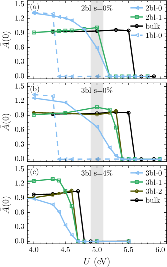
Focusing now on the 2- and 3-bilayer slabs (Fig. 7a and b), one can see that the shift of quickly becomes weaker as the slab thickness increases. For the 2-bilayer slab, shown in Fig. 7a, is only about 0.4 eV smaller than in the bulk case, while for the 3-bilayer slab (Fig. 7b) is only 0.2 eV smaller than in the bulk. Thus, our results indicate that at , the 3-bilayer slab will already be metallic, similar to the bulk system, while 2-bilayers are just on the verge of the MIT. However, in both cases, the surface layer exhibits a notably different behavior compared to the inner or subsurface layers. Even though the corresponding becomes zero at essentially the same value as the inner layers, the transition appears to be more continuous in the surface layer. In addition, the occupations in the surface layer exhibit strong orbital polarization already below (see Fig. 9a for ), consistent with the large crystal-field splitting in the surface layer depicted in Fig. 5a, whereas the inner and subsurface layers are only weakly polarized, similar to the bulk case.
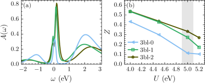
To further analyze the different behavior of the surface, Fig. 8a shows layer-resolved spectral functions for the 3-bilayer slab at . It can be seen, that in particular the inner, but also to a large extent the subsurface layer, exhibits a spectral function that is very similar to the bulk (shown in Fig. 3c). In contrast, the quasiparticle peak in the surface layer is much narrower, and there is a stronger transfer of spectral weight into the upper and lower Hubbard bands, which are significantly more pronounced than for the subsurface and inner layers. The strongly reduced spectral weight of the quasiparticle peak at the surface also follows from the behavior of the inverse quasiparticle mass enhancement, , shown as function of in Fig. 8b, which is consistently smaller in the surface layer than in the other two layers, and is nearly vanishing for . Here, is estimated from the imaginary part of the self-energy at the lowest Matsubara frequency (c.f. [46]):
| (1) |
All this indicates that correlation effects are strongly enhanced at the surface relative to the inner layers, in good agreement with experimental observations for CaVO3 and the closely related material SrVO3 [33; 34; 51; 52] and previous DFT+DMFT calculations for SrVO3 [35; 53]. In particular, close to but still in the metallic phase, the surface seems to form a “dead layer”, with nearly vanishing quasiparticle weight, as discussed in Ref. 54 based on DMFT calculations for a one-band Hubbard model within a slab geometry.
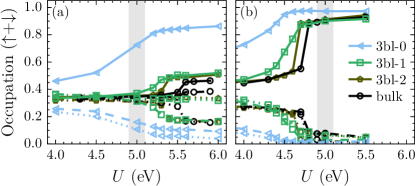
Finally, we also consider the combined effect of finite thickness and tensile epitaxial strain. We focus on the case of a 3-bilayer slab with 4 % tensile strain, shown in Fig. 7c. Similar to the case of the strained bulk systems, tensile strain leads to a strong shift of to lower values also in the strained 3-bilayer slab, resulting in an insulating state at . Moreover, comparing to the bulk reference at 4 % tensile strain, one can see that the effect of the reduced thickness is rather weak, as was the case in the corresponding unstrained system. Again, the surface layer exhibits a more continuous change of but maintains essentially the same as the inner layers. From the orbital occupations shown in Fig. 9, it can be seen that in the strained slab all layers are strongly polarized in the insulating state. Thereby, the behavior of the inner layers is very similar to the corresponding strained bulk system (compare Fig. 9b with Fig. 3b) whereas the surface layer is already strongly polarized in the metallic phase. This is again fully consistent with the calculated crystal-field splitting between the MLWFs, shown in Fig. 5b. The splitting in the inner and subsurface layers of the strained 3-bilayer slab is very similar to the bulk splitting under 4 % tensile strain, while in the surface layer this splitting is further enhanced.
It thus appears that in all cases the MIT is mainly controlled by the local crystal-field splitting within the manifold and the resulting tendency to form an orbitally polarized insulating state. As seen in Fig. 5 the crystal-field splitting in all layers is strongly affected by tensile epitaxial strain, whereas the finite size effects seem to manifest mostly as an enhanced crystal-field splitting in the surface layer. The insulating character of the unstrained 1-bilayer slab therefore appears more like a surface-induced effect rather than being related to the formation of quantum well states along the direction. Even though a peak structure related to such quantum well states is clearly visible in the DFT-DOS of the inner layers of the 3-bilayer slab (see Fig. 4), this does not seem to have a big impact on the metallic character.
We note that in Ref. 20 we found that, while the crystal-field splitting can nicely explain the trends in for a system under tensile strain, the strain-induced changes in the hopping amplitudes also have to be taken into account to obtain the correct magnitude of the shift in . In contrast, for the finite size effect discussed here, the hopping amplitudes appear to be less relevant, since, as noted previously, they do not exhibit any significant changes with reduced thickness.
V Summary and conclusions
In summary, we have used DFT+DMFT calculations to compare the effects of tensile epitaxial strain and finite film thickness on the tendency of CaVO3 to undergo a Mott MIT. We find that tensile strain strongly decreases , the critical interaction strength for the Mott transition, and that strains of the order of what is achievable in a fully strained CaVO3 film grown on SrTiO3 (about 3.5 %) are sufficient to induce a transiton to the Mott-insulating state. Alternatively. a transition to the insulating state can also be achieved in ultrathin free-standing slabs of CaVO3, however, only for thicknesses smaller than approximately 4 perovskite units. In contrast, a 6-layer slab already exhibits bulk-like behavior.
Furthermore, we observe a strong suppression of the quasiparticle weight in the surface layer, consistent with previous experimental and theoretical reports for CaVO3 and SrVO3. This is due to a strong surface-induced crystal-field splitting, which results in strong orbital polarization inside the surface layer. Our results show that these modifications are essentially restricted to the outermost layer and that the bulk properties are nearly recovered already in the subsurface layer.
Our results demonstrate that the effects of tensile epitaxial strain and the finite size or surface effects cooperate, but that the strain effect clearly dominates, except in the ultra-thin limit (i.e., below 4 perovskite layers). Since in Ref. 9 insulating behavior was observed for a thickness of up to 4 nm, i.e., 10-11 perovskite layers, this suggests that factors other than pure finite size effects are at play here. The scenario outlined in Sec. I, i.e., a strain-induced insulating state in the fully strained thinnest films, which evolves back to metallic bulk behavior in thicker films where the epitaxial strain is relaxed, provides a potential alternative explanation for these experimental observations. However, other factors, not considered in this work, could also be of importance, such as, e.g., point defects, interface roughness, or other forms of disorder, which could then also lead to an insulating state via Anderson localization. Further experimental studies are required to clarify this. Nevertheless, we point out that the thickness of approximately 4 perovskite units, for which we find the CaVO3 slabs to be just at the border of the MIT, is in very good agreement with the thickness of 2-3 monolayers, for which a gap opening was observed by photoemission spectroscopy in SrVO3 films grown by molecular beam epitaxy [7]. Furthermore, in Ref. 12 it was shown that the critical thickness for the formation of an insulating state in La2/3Ca1/3MnO3 can be reduced to only 3 unit cells by minimizing the substrate-induced strain as well as the amount of oxygen vacancies. Thus, our results for the unstrained slabs can be considered as providing a lower limit for the thickness above which a metallic state can be preserved in CaVO3, as long as other effects promoting the insulating state can be excluded.
Finally, our study shows that it is possible to tune the Mott transition in CaVO3 (and related materials) through multiple control parameters. This provides an exciting avenue for the design of Mott transistors [55; 56] and other “Mott-tronic” devices [57], or also to tune the properties of correlated metals for other potential applications, e.g., as transparent conductors [58].
Acknowledgements.
This research was supported by the NCCR MARVEL, funded by the Swiss National Science Foundation. The authors thank Daniel McNally, Milan Radovic, and Thorsten Schmitt for insightful discussions. Calculations have been performed on “Piz Daint” at the Swiss National Supercomputing Centre.References
- Cheong [2007] S.-W. Cheong, Nature Materials 6, 927 (2007).
- Dagotto and Tokura [2008] E. Dagotto and Y. Tokura, MRS Bulletin 33, 1037 (2008).
- Imada et al. [1998] M. Imada, A. Fujimori, and Y. Tokura, Reviews of Modern Physics 70, 1039 (1998).
- Mannhart and Schlom [2010] J. Mannhart and D. G. Schlom, Science 327, 1607 (2010).
- Hwang et al. [2012] H. Y. Hwang, Y. Iwasa, M. Kawasaki, B. Keimer, N. Nagaosa, and Y. Tokura, Nature Materials 11, 103 (2012).
- Ohtomo and Hwang [2004] A. Ohtomo and H. Y. Hwang, Nature 427, 423 (2004).
- Yoshimatsu et al. [2010] K. Yoshimatsu, T. Okabe, H. Kumigashira, S. Okamoto, S. Aizaki, A. Fujimori, and M. Oshima, Physical Review Letters 104, 147601 (2010).
- Gu et al. [2014] M. Gu, S. A. Wolf, and J. Lu, Advanced Materials Interfaces 1, 1300126 (2014).
- Gu et al. [2013] M. Gu, J. Laverock, B. Chen, K. E. Smith, S. A. Wolf, and J. Lu, Journal of Applied Physics 113, 133704 (2013).
- Wong et al. [2010] F. J. Wong, S.-H. Baek, R. V. Chopdekar, V. V. Mehta, H.-W. Jang, C.-B. Eom, and Y. Suzuki, Physical Review B 81, 161101 (2010).
- He et al. [2012] C. He, T. D. Sanders, M. T. Gray, F. J. Wong, V. V. Mehta, and Y. Suzuki, Physical Review B 86, 081401 (2012).
- Liao et al. [2015] Z. Liao, F. Li, P. Gao, L. Li, J. Guo, X. Pan, R. Jin, E. W. Plummer, and J. Zhang, Physical Review B 92, 125123 (2015).
- Liu et al. [2010] J. Liu, M. Kareev, B. Gray, J. W. Kim, P. Ryan, B. Dabrowski, J. W. Freeland, and J. Chakhalian, Applied Physics Letters 96, 233110 (2010).
- Scherwitzl et al. [2011] R. Scherwitzl, S. Gariglio, M. Gabay, P. Zubko, M. Gibert, and J.-M. Triscone, Physical Review Letters 106, 246403 (2011).
- Catalano et al. [2014] S. Catalano, M. Gibert, V. Bisogni, O. E. Peil, F. He, R. Sutarto, M. Viret, P. Zubko, R. Scherwitzl, A. Georges, and et al., APL Materials 2, 116110 (2014).
- Wang et al. [2015] L. Wang, S. Ju, L. You, Y. Qi, Y. wei Guo, P. Ren, Y. Zhou, and J. Wang, Scientific Reports 5, 18707 (2015).
- Biswas et al. [2014] A. Biswas, K.-S. Kim, and Y. H. Jeong, Journal of Applied Physics 116, 213704 (2014).
- Okamoto [2011] S. Okamoto, Physical Review B 84, 201305 (2011).
- Zhong et al. [2013] Z. Zhong, Q. Zhang, and K. Held, Physical Review B 88, 125401 (2013).
- Sclauzero et al. [2016] G. Sclauzero, K. Dymkowski, and C. Ederer, Physical Review B 94, 245109 (2016).
- Dymkowski and Ederer [2014] K. Dymkowski and C. Ederer, Physical Review B 89, 161109 (2014).
- Falcón et al. [2004] H. Falcón, J. A. Alonso, M. T. Casais, M. J. Martínez-Lope, and J. Sánchez-Benítez, Journal of Solid State Chemistry 177, 3099 (2004).
- Nekrasov et al. [2005] I. A. Nekrasov, G. Keller, D. E. Kondakov, A. V. Kozhevnikov, T. Pruschke, K. Held, D. Vollhardt, and V. I. Anisimov, Physical Review B 72, 155106 (2005).
- Yoshida et al. [2010] T. Yoshida, M. Hashimoto, T. Takizawa, A. Fujimori, M. Kubota, K. Ono, and H. Eisaki, Physical Review B 82, 085119 (2010).
- Liberati et al. [2009] M. Liberati, R. Chopdekar, V. Mehta, E. Arenholz, and Y. Suzuki, Journal of Magnetism and Magnetic Materials 321, 2852 (2009).
- Freund [1992] L. B. Freund, MRS Bulletin 17, 52 (1992).
- Georges et al. [1996] A. Georges, G. Kotliar, W. Krauth, and M. J. Rozenberg, Reviews of Modern Physics 68, 13 (1996).
- Anisimov et al. [1997] V. I. Anisimov, A. I. Poteryaev, M. A. Korotin, A. O. Anokhin, and G. Kotliar, J. Phys.: Condens. Matter 9, 7359 (1997).
- Lechermann et al. [2006] F. Lechermann, A. Georges, A. Poteryaev, S. Biermann, M. Posternak, A. Yamasaki, and O. K. Andersen, Physical Review B 74, 125120 (2006).
- Held [2007] K. Held, Advances in Physics 56, 829 (2007).
- Pavarini et al. [2004] E. Pavarini, S. Biermann, A. Poteryaev, A. I. Lichtenstein, A. Georges, and O. K. Andersen, Physical Review Letters 92, 176403 (2004).
- Zhong et al. [2015] Z. Zhong, M. Wallerberger, J. M. Tomczak, C. Taranto, N. Parragh, A. Toschi, G. Sangiovanni, and K. Held, Physical Review Letters 114, 246401 (2015).
- Maiti et al. [2001] K. Maiti, D. D. Sarma, M. J. Rozenberg, I. H. Inoue, H. Makino, O. Goto, M. Pedio, and R. Cimino, Europhysics Letters (EPL) 55, 246 (2001).
- Eguchi et al. [2006] R. Eguchi, T. Kiss, S. Tsuda, T. Shimojima, T. Mizokami, T. Yokoya, A. Chainani, S. Shin, I. H. Inoue, T. Togashi, S. Watanabe, C. Q. Zhang, C. T. Chen, M. Arita, K. Shimada, H. Namatame, and M. Taniguchi, Physical Review Letters 96, 076402 (2006).
- Liebsch [2003] A. Liebsch, Physical Review Letters 90, 096401 (2003).
- Giannozzi et al. [2009] P. Giannozzi, S. Baroni, N. Bonini, M. Calandra, R. Car, C. Cavazzoni, D. Ceresoli, G. L. Chiarotti, M. Cococcioni, I. Dabo, A. D. Corso, S. de Gironcoli, S. Fabris, G. Fratesi, R. Gebauer, U. Gerstmann, C. Gougoussis, A. Kokalj, M. Lazzeri, L. Martin-Samos, N. Marzari, F. Mauri, R. Mazzarello, S. Paolini, A. Pasquarello, L. Paulatto, C. Sbraccia, S. Scandalo, G. Sclauzero, A. P. Seitsonen, A. Smogunov, P. Umari, and R. Wentzcovitch, Journal of Physics: Condensed Matter 21, 395502 (2009).
- Perdew et al. [1996] J. P. Perdew, K. Burke, and M. Ernzerhof, Physical Review Letters 77, 3865 (1996).
- Sclauzero and Ederer [2015] G. Sclauzero and C. Ederer, Physical Review B 92, 235112 (2015).
- Marzari et al. [2012] N. Marzari, A. A. Mostofi, J. R. Yates, I. Souza, and D. Vanderbilt, Reviews of Modern Physics 84, 1419 (2012).
- Mostofi et al. [2008] A. A. Mostofi, J. R. Yates, Y.-S. Lee, I. Souza, D. Vanderbilt, and N. Marzari, Computer Physics Communications 178, 685 (2008).
- Pavarini et al. [2005] E. Pavarini, A. Yamasaki, J. Nuss, and O. K. Andersen, New J. Phys. 7, 188 (2005).
- Parcollet et al. [2015] O. Parcollet, M. Ferrero, T. Ayral, H. Hafermann, I. Krivenko, L. Messio, and P. Seth, Computer Physics Communications 196, 398 (2015).
- Aichhorn et al. [2016] M. Aichhorn, L. Pourovskii, P. Seth, V. Vildosola, M. Zingl, O. E. Peil, X. Deng, J. Mravlje, G. J. Kraberger, C. Martins, and et al., Computer Physics Communications 204, 200 (2016).
- Gull et al. [2011] E. Gull, A. J. Millis, A. I. Lichtenstein, A. N. Rubtsov, M. Troyer, and P. Werner, Reviews of Modern Physics 83, 349 (2011).
- Seth et al. [2016] P. Seth, I. Krivenko, M. Ferrero, and O. Parcollet, Computer Physics Communications 200, 274 (2016).
- Fuchs et al. [2011] S. Fuchs, E. Gull, M. Troyer, M. Jarrell, and T. Pruschke, Physical Review B 83, 235113 (2011).
- Jarrell and Gubernatis [1996] M. Jarrell and J. E. Gubernatis, Physics Reports 269, 133 (1996).
- Rondinelli and Spaldin [2011] J. M. Rondinelli and N. A. Spaldin, Advanced Materials 23, 3363 (2011).
- Note [1] We note that here we are using a simplified notation where R and R’ do not necessarily correspond to lattice translations of the structure. Thus, strictly speaking, these matrix elements can depend on both R and . However, since all V sites are equivalent, one can always find a local transformation such that the matrix elements for different R become identical.
- Lu et al. [2016] D. Lu, D. J. Baek, S. S. Hong, L. F. Kourkoutis, Y. Hikita, and H. Y. Hwang, Nature Materials 15, 1255 (2016).
- Laverock et al. [2013] J. Laverock, B. Chen, K. E. Smith, R. P. Singh, G. Balakrishnan, M. Gu, J. W. Lu, S. A. Wolf, R. M. Qiao, W. Yang, and J. Adell, Physical Review Letters 111, 047402 (2013).
- Laverock et al. [2015] J. Laverock, J. Kuyyalil, B. Chen, R. P. Singh, B. Karlin, J. C. Woicik, G. Balakrishnan, and K. E. Smith, Physical Review B 91, 165123 (2015).
- Ishida et al. [2006] H. Ishida, D. Wortmann, and A. Liebsch, Physical Review B 73, 245421 (2006).
- Borghi et al. [2009] G. Borghi, M. Fabrizio, and E. Tosatti, Physical Review Letters 102, 066806 (2009).
- Newns et al. [1998] D. M. Newns, J. A. Misewich, C. C. Tsuei, A. Gupta, B. A. Scott, and A. Schrott, Applied Physics Letters 73, 780 (1998).
- Inoue and Rozenberg [2008] I. H. Inoue and M. J. Rozenberg, Advanced Functional Materials 18, 2289 (2008).
- Yang et al. [2011] Z. Yang, C. Ko, and S. Ramanathan, Annual Review of Materials Research 41, 337 (2011).
- Zhang et al. [2016] L. Zhang, Y. Zhou, L. Guo, W. Zhao, A. Barnes, H.-T. Zhang, C. Eaton, Y. Zheng, M. Brahlek, H. F. Haneef, N. J. Podraza, M. H. W. Chan, V. Gopalan, K. M. Rabe, and R. Engel-Herbert, Nature Materials 15, 204 (2016).