Mask aligner for ultrahigh vacuum with capacitive distance control
Abstract
We present a mask aligner driven by three piezo motors which guides and aligns a SiN shadow mask under capacitive control towards a sample surface. The three capacitors for read out are located at the backside of the thin mask such that the mask can be placed in m distance from the sample surface, while keeping it parallel to the surface. Samples and masks can be exchanged in-situ and the mask can additionally be displaced parallel to the surface. We demonstrate an edge sharpness of the deposited structures below 100 nm, which is likely limited by the diffusion of the deposited Au on Si(111).
Lateral nanostructuring is the base of a multifold of experimental research areas, such as mesoscopics, solid-state based quantum computing, nanoelectromechanical systems (NEMS), or photonics. Mostly, electron beam or optical lithography are employed, wherein the use of solvent-based resists inevitably leaves residues, which compromise the surface quality.
This is detrimental for surface science techniques in ultrahigh vacuum (UHV) such as scanning tunneling microscopy (STM).
An appealing alternative within UHV is the bottom-up assembly of individual atoms Lyo and Avouris (1991); Eigler and Schweizer (1990); Custance, Perez, and Morita (2009); Crommie, Lutz, and Eigler (1993). It has been automatedCelotta et al. (2014); Kalff et al. (2016) and has even been combined with mesoscopic device technologyVasko et al. (2011); Fuechsle et al. (2012). The method is extremely precise at the atomic level Loth et al. (2012); Khajetoorians et al. (2013); Choi et al. (2017) and can be stable up to room temperature for certain types of manipulation schemesShen et al. (1995). However, it becomes increasingly tedious for more complex mesoscopic structures.
A faster alternative, which avoids chemical resists, is direct imprinting of structures by an atomic force microscopeGarcia, Knoll, and Riedo (2014). However, the corresponding lithography is restricted to selected materials and, typically, requires an environment which is not compatible with UHV. An example for the latter is local anodic oxidationDagata et al. (1990), a single-step nanolithography with sub-10 nm resolution.Garcia, Martinez, and Martinez (2006) It has been applied, e.g., to fabricate mesoscopic structures in GaAs Fuhrer et al. (2001) or graphene Puddy, Chua, and Buitelaar (2013); Magda et al. (2014).
However, since oxidation is the essential step, this technique lacks versatility in terms of materials.
Some UHV-based methods for nanostructuring are even more focused to a particular material as, e.g., the defect charging of BN below graphene Lee et al. (2016), which recently enabled ultraclean graphene quantum dots of mesoscopic size to be probed by STM Ghahari et al. (2017).
A more versatile alternative for UHV nanostructuring is shadow mask evaporation, also called stencil lithographyDu et al. (2017). Silicon-based shadow masks have been produced with feature sizes less than 10 nmDeshmukh et al. (1999) employing e-beam lithographyOno et al. (1996), focussed ion beam lithographyMatsui and Ochiai (1996), or, with larger throughput, ultraviolet optical lithographyvan den Boogaart et al. (2004). The central challenge beyond the mask production is to bring the mask close enough to the substrate in order to minimize the penumbra during evaporation.
The most simple solution is a rigid placement of the mask with respect to the substrateGärtner et al. (2006). However, here the mask-sample distance is either limited to tens of m Stöffler and Hoffmann-Vogel (2015), or the mask structure is in direct contact with the substrateStaley et al. (2007); Tien et al. (2016). The latter has the drawbacks of possible additional contamination of the substrate Linklater and Nogami (2008) and difficulties to remove the mask in UHV. Another solution is based on the cantilever from a scanning force microscope (SFM). The SFM tip senses the surface while carrying the mask on top Lüthi et al. (1999); Egger et al. (2005). This led to structures, evaporated through the mask, with edge sharpness down to 10 nm Egger et al. (2005), but comes with the instrumental overhead of a fully operational SFM. Finally, piezomotors have been utilized to move either the sample Zahl et al. (2005) or the mask Savu et al. (2008) in all three dimensions. However, so far, the distance calibration in the small distance range required an initial touching of the mask to the substrate, before the distance can be monitored, e.g., by a field emission current Steurer et al. (2014). Again, an edge sharpness in the 10 nm range has been achieved, where diffusion of the deposited material is likely the limiting factor Tun et al. (2007); Linklater and Nogami (2008).
Here, we present a capacitively controlled UHV mask aligner employing three piezo motors for approaching the mask to the substrate. Since the three capacitive sensors are placed directly on the backside of the 1 m thick SiN mask, the mask can be aligned with sub-m precision relative to the substrate on a lateral scale of millimeters. This approach avoids an initial touching of the mask to the sample and requires less instrumental complexity than the SFM based technique. Lateral movement of the substrate relative to the mask (dynamical stencil lithography)Du et al. (2017), is enabled by an additional, horizontal piezo motor. We show that sub-100 nm edge sharpness is possible with this UHV mask aligner, while edge sharpness partly goes down to 10 nm. Likely, both values are limited by the diffusion of Au on the oxidized Si(111) substrate.Linklater and Nogami (2008)
A geometrical estimate clarifies the required precision in distance control: For a distance between evaporation source and mask, distance between mask and substrate, and lateral extension of the evaporation source , one gets a penumbra width of the evaporated structures:Linklater and Nogami (2008) , assuming a ballistic path of the atoms from the evaporation source to the substrate. Hence, at typical m and mm, as used in our experiment (see below), a penumbra width nm requires nm. A conservative estimate of the mean free path within the molecular beam is given by the value for an ideal gasReichl (1980); Farrow (1995)
| (1) |
at temperature , deposition rate , atomic mass , density of the deposited material , and atomic scattering diameter .
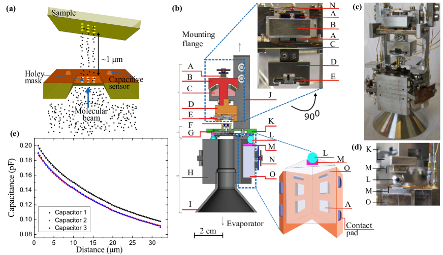
Hence, is in the range of 100 m at typical deposition rates of Å/s, confirming the ballistic regime. Figure 1(a) shows a sketch of the mask and the sample. Three capacitive sensors are symmetrically placed around the mask with a mutual distance of 1 mm. They enable high precision control of the distance to a conductive substrate, while adjusting the mask parallel to the sample surface.
The approach of the mask to the substrate is realized by three piezo motors. A cross section of the corresponding mask aligner is shown in Fig. 1(b).
It consists of three modules made from stainless steel. The lower motor module (H, I, M, N, O) contains the three piezoelectric motors (lower inset) Pan et al. (1990); Pan (1993) and enables mounting of the mask aligner to a CF flange. The piezomotors are assembled in three V-shaped recesses of the lower frame (H), being placed at a relative angle of . Each motor consists of a sapphire prism (O) with an equilateral triangular base of 10 mm edge length. The prism is clamped to the recess over four piezoelectric stacks (PI Ceramic GmbH) (A) covered each by a polished Al2O3 plate. Two further piezo-stacks are clamped to the front-end of the sapphire prism via a pressure plate (N). The pressure on this plate is adjusted via a screw, which strains the 0.2 mm thick CuBe spring contacting the plate via a ruby ball (diameter: 2 mm).Wiebe et al. (2004) Each prism, hence, can be moved via slip-stick motion employing a simultaneous saw-tooth voltage to all six piezo-stacks. Importantly, each of the three piezomotors can be moved independently. Step sizes during the movement mainly depend on the amplitude of the sawtooth voltage ( V) and the spring tension. They are typically in the range 50-200 nm as measured by a ruler after consecutive steps. The maximum vertical displacement of each motor amounts to 9.5 mm.
The central mask module (F, G, K) lies on top of the three prisms via three magnetic Nd spheres (L) (Fig. 1(d)). Each sphere is magnetically attached to the frame of the mask stage (K) and a prism (O) via Ni plates (M) glued to prism and frame. Small grooves in the Ni plates allow horizontal adjustment of the sphere. The sphere shape enables an inclination of the mask stage with respect to the individual piezomotors as required for the deliberate mask alignment. The frame (K) carries the mask stage, which allows exchange of
the mask via a standard sample holder of size mm2.
Both frames (H, K) are pierced by a hole with a diameter of 12 mm enabling the molecular beam to hit the mask. A metal cone (I) prevents evaporation of material
on the piezo-stacks and prisms.
The upper sample module (AE, J and upper inset) can move the sample parallel to the mask. It consists of a T-shaped stainless steel slider (B) holding the sample stage (D) and sliding via an additional piezomotor across a fixed sapphire rail (C). A horizontal range of 3.3 mm is possible. Sample holder (E) and sample stage (D) are electrically isolated in order to reduce stray capacitances, since the sample surface acts as the counter electrode for the capacitive sensors on the mask (Fig. 1(a)). The sample can be exchanged in-situ via a standard sample holder of size mm2.
Typical capacitance curves of the three sensors on the mask during an approach to a HOPG sample are shown in Fig. 1(e). They are measured employing an ac voltage while reading out the current response via a lock-in amplifier, leading to a sensitivity of fF. The mask-sample distance is calibrated via the step size of the piezomotor (see above) and the contact point between mask and sample ( m), which is taken as the point, where the curve starts to saturate at small distances. The curves of Fig. 1(e) can be nicely fitted by with , , and being fit parameters. The deviation from the naively expected behavior (: area of capacitor, (): dielectric constant of vacuum (material)) is related to remaining stray capacitances, which also can exhibit a dependence. In order to minimize these stray capacitances, cables are shielded (also to avoid crosstalk) and contacts to the capacitive plates are provided from the backside. Since the capacitive sensors are ending at the backside of the 1 m thick Si3N4 mask, there is an additional vertical offset m in , which contributes to .
Obviously, the capacitive control can start at distances m, which can be easily determined optically within UHV using a long-distance microscope.Geringer et al. (2009) To compare the measured capacitance with the naively expected capacitance at m, we use the front end size of the capacitive sensor m2, the dielectric constant of Si3N4, and the offset m, revealing fF. This is slightly smaller than the measured value of about fF. Hence, stray capacitances still contribute. Indeed, we find variations in the values for different masks by up to a factor of four. Nevertheless, distances corresponding to a single step of the piezomotor can always be detected reliably at m. Such a single step of one piezo motor corresponds to lifting of one of the capacitive sensors by nm with respect to the others or to an angular misalignment of . This enables an extremely high precision of parallel alignment. To minimize the distance between mask and sample without touching, we approached ten different masks until contact showing that the gradient of the capacitance is a reliable measure, i.e., if fF/m, the mask does not touch and is closer than m to the
substrate. Note that the uncertainty of m in distance between the different capacitors still provides an angular precision of .
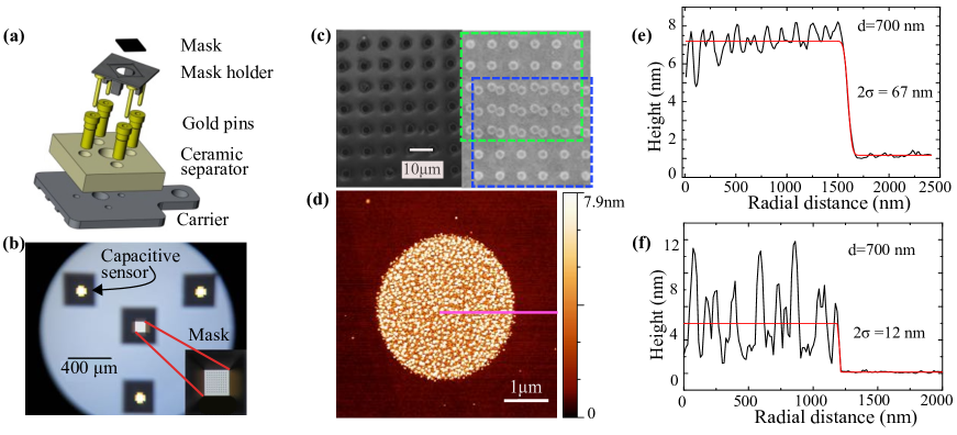
Fig. 2(a) shows a sketch of the mask assembly enabling capacitive control and in-situ mask exchange. The mask carrier is a mm3 steel plate compatible with existing transfer mechanisms in UHV (Scienta Omicron). The mask structure ( mm3) is glued to a mask holder carrying four gold pins at the underside, which are used to contact the capacitive sensor and ground. These gold pins are inserted into the four socket type gold pins mounted to the mask carrier, which provide electrical contacts to springs in the mask stage when the carrier is inserted.
The top view of the shadow mask (Norcada Inc.) is shown in Fig. 2(b) and (c). It consists of a 1 m thick Si3N4 membrane of size (100 m)2 carried by a highly doped Si wafer ( cm) of 0.2 mm thickness. The membrane is produced by depositing and structuring Si3N4 on top of the wafer and, subsequently, etching holes into the Si from the back. In the same etching step the three holes for the capacitors are produced which are covered by the same Si3N4 membrane, but without structure. Afterwards, 100 nm of SiO2 and 100 nm of CrAu are deposited on the backside of these unstructured membranes. Each of the resulting thin capacitive CrAu plates is glued to a Au wire, which contacts to the gold pin of the mask holder. The inner membrane called mask in Fig. 2(b) is pierced by an array of holes with diameter 3 m (Fig. 2(c), left).
Using this mask, we performed test evaporations of Au on a Si(111) sample at room temperature. The sample was prepared by ultrasonication in acetone and isopropyl alcohol, followed by oxygen plasma etching at 40 W. The piezo motors are calibrated ex-situ revealing error bars in the step size of about 5 %. Consecutive fields of circles are evaporated through the mask at a rate Å/s and at pressure Pa. Between the fields, the sample is moved closer to the mask and offset horizontally by m using the piezo motors. Figure 2c (right) displays a scanning electron microscopy (SEM) image of two overlapping fields, which have been used to crosscheck the steps of the horizontal piezo motor, revealing a discrepancy of only 4 % with respect to the ex-situ calibration ( nm per step at amplitude 60 V).
The evaporated circles are subsequently imaged by SFM. Figure 2(d) shows such a SFM image after evaporation at nm. The circle with 7 nm height consists of multiple clusters with diameters of nm. It exhibits sharp edges, and a flat, clean surrounding, which reveals a successful transfer of the holey mask structure to the sample. The edge sharpness is basically determined by the cluster sizes (left inset in Fig. 3). Individual profile lines reveal an edge sharpness of nm (Fig. 2(f)). To quantify the edge sharpness, we angularly averagedHorcas et al. (2007) the profile lines from the center of the disk towards its rim (pink line in Fig. 2(d)) and fitted an error function to them (Fig. 2(e)).
Note that although ellipticity is limited to a cluster size in our case, the angular average is very sensitive to possible lateral drifts of the mask relative to the sample, which would lead to an elliptical shape of the evaporated structures.
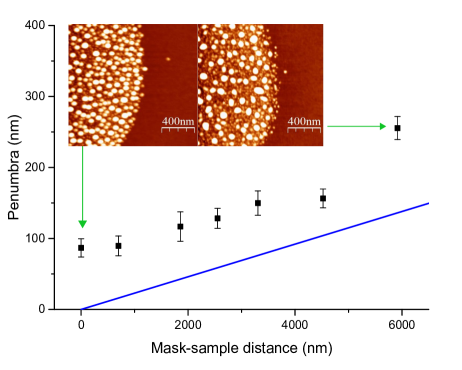
Figure 3 shows the 2 widths of the fitted error functions as a function of . The error bar includes the variations between different circles, which are deposited simultaneously. The theoretical limit according to is provided for comparison (blue line). The offset of the data points with respect to the blue line is obviously close to the cluster size, implying that it is limited by diffusion. A diffusion induced broadening of nm has recently also been found for Au evaporation on Si(001) at room temperature , after pressing a shadow mask directly onto the sample Linklater and Nogami (2008). We note that even at the safe approach distance of m, the penumbra size is nm.
In conclusion, we described a novel type of UHV mask aligner employing piezo motors and a capacitive control for mask-sample alignment. We demonstrate edge sharpness down to 10 nm and edge precision below 100 nm, possibly limited by diffusion of Au on Si(111) at room temperature. The versatility of the mask aligner is given by the in-situ mask and sample exchange and the lateral movement of the sample relative to the mask.
References
- Lyo and Avouris (1991) I.-W. Lyo and P. Avouris, Science 253, 173 (1991).
- Eigler and Schweizer (1990) D. M. Eigler and E. K. Schweizer, Nature 344, 524 (1990).
- Custance, Perez, and Morita (2009) O. Custance, R. Perez, and S. Morita, Nature Nanotechnology 4, 803 (2009).
- Crommie, Lutz, and Eigler (1993) M. F. Crommie, C. P. Lutz, and D. M. Eigler, Science 262, 218 (1993).
- Celotta et al. (2014) R. J. Celotta, S. B. Balakirsky, A. P. Fein, F. M. Hess, G. M. Rutter, and J. A. Stroscio, Review of Scientific Instruments 85, 121301 (2014).
- Kalff et al. (2016) F. E. Kalff, M. P. Rebergen, E. Fahrenfort, J. Girovsky, R. Toskovic, J. L. Lado, J. Fernández-Rossier, and A. F. Otte, Nature Nanotechnology 11, 926 (2016).
- Vasko et al. (2011) S. E. Vasko, A. Kapetanovic, V. Talla, M. D. Brasino, Z. Zhu, A. Scholl, J. D. Torrey, and M. Rolandi, Nano Letters 11, 2386 (2011).
- Fuechsle et al. (2012) M. Fuechsle, J. A. Miwa, S. Mahapatra, H. Ryu, S. Lee, O. Warschkow, L. C. L. Hollenberg, G. Klimeck, and M. Y. Simmons, Nat. Nanotechnol. 7, 242 (2012).
- Loth et al. (2012) S. Loth, S. Baumann, C. P. Lutz, D. M. Eigler, and A. J. Heinrich, Science 335, 196 (2012).
- Khajetoorians et al. (2013) A. A. Khajetoorians, B. Baxevanis, C. Hubner, T. Schlenk, S. Krause, T. O. Wehling, S. Lounis, A. Lichtenstein, D. Pfannkuche, J. Wiebe, and R. Wiesendanger, Science 339, 55 (2013).
- Choi et al. (2017) T. Choi, W. Paul, S. Rolf-Pissarczyk, A. J. Macdonald, F. D. Natterer, K. Yang, P. Willke, C. P. Lutz, and A. J. Heinrich, Nat. Nanotechnol. 12, 420 (2017).
- Shen et al. (1995) T. C. Shen, C. Wang, G. C. Abeln, J. R. Tucker, J. W. Lyding, P. Avouris, and R. E. Walkup, Science 268, 1590 (1995).
- Garcia, Knoll, and Riedo (2014) R. Garcia, A. W. Knoll, and E. Riedo, Nature Nanotechnology 9, 577 (2014).
- Dagata et al. (1990) J. A. Dagata, J. Schneir, H. H. Harary, C. J. Evans, M. T. Postek, and J. Bennett, Applied Physics Letters 56, 2001 (1990).
- Garcia, Martinez, and Martinez (2006) R. Garcia, R. V. Martinez, and J. Martinez, Chem. Soc. Rev. 35, 29 (2006).
- Fuhrer et al. (2001) A. Fuhrer, S. Lüscher, T. Ihn, T. Heinzel, K. Ensslin, W. Wegscheider, and M. Bichler, Nature 413, 822 (2001).
- Puddy, Chua, and Buitelaar (2013) R. K. Puddy, C. J. Chua, and M. R. Buitelaar, Applied Physics Letters 103, 183117 (2013).
- Magda et al. (2014) G. Z. Magda, X. Jin, I. Hagymási, P. Vancsó, Z. Osváth, P. Nemes-Incze, C. Hwang, L. P. Biró, and L. Tapasztó, Nature 514, 608 (2014).
- Lee et al. (2016) J. Lee, D. Wong, J. V. Jr, J. F. Rodriguez-Nieva, S. Kahn, H.-Z. Tsai, T. Taniguchi, K. Watanabe, A. Zettl, F. Wang, L. S. Levitov, and M. F. Crommie, Nature Physics 12, 1032 (2016).
- Ghahari et al. (2017) F. Ghahari, D. Walkup, C. Gutiérrez, J. F. Rodriguez-Nieva, Y. Zhao, J. Wyrick, F. D. Natterer, W. G. Cullen, K. Watanabe, T. Taniguchi, L. S. Levitov, N. B. Zhitenev, and J. A. Stroscio, Science 356, 845 (2017).
- Du et al. (2017) K. Du, J. Ding, Y. Liu, I. Wathuthanthri, and C.-H. Choi, Micromachines 8, 131 (2017).
- Deshmukh et al. (1999) M. M. Deshmukh, D. C. Ralph, M. Thomas, and J. Silcox, Applied Physics Letters 75, 1631 (1999).
- Ono et al. (1996) K. Ono, H. Shimada, S. ichi Kobayashi, and Y. Ootuka, Japanese Journal of Applied Physics 35, 2369 (1996).
- Matsui and Ochiai (1996) S. Matsui and Y. Ochiai, Nanotechnology 7, 247 (1996).
- van den Boogaart et al. (2004) M. A. F. van den Boogaart, G. M. Kim, R. Pellens, J.-P. van den Heuvel, and J. Brugger, Journal of Vacuum Science & Technology B: Microelectronics and Nanometer Structures 22, 3174 (2004).
- Gärtner et al. (2006) C. Gärtner, R. Hoffman, F. Pérez-Willard, M. Sauter, C. Sürgers, and H. v. Löhneysen, Rev. Sci. Instr. 77, 026101 (2006).
- Stöffler and Hoffmann-Vogel (2015) D. Stöffler and R. Hoffmann-Vogel, J. Vac. Sci. Technol. B 33, 013201 (2015).
- Staley et al. (2007) N. Staley, H. Wang, C. Puls, J. Forster, T. N. Jackson, K. McCarthy, B. Clouser, and Y. Liu, Applied Physics Letters 90, 143518 (2007).
- Tien et al. (2016) D. H. Tien, J.-Y. Park, K. B. Kim, N. Lee, and Y. Seo, Scientific Reports 6, 25050 (2016).
- Linklater and Nogami (2008) A. Linklater and J. Nogami, Nanotechnol. 19, 285302 (2008).
- Lüthi et al. (1999) R. Lüthi, R. R. Schlittler, J. Brugger, P. Vettiger, M. E. Welland, and J. K. Gimzewski, Appl. Phys. Lett. 75, 1314 (1999).
- Egger et al. (2005) S. Egger, A. Ilie, Y. Fu, J. Chongsathien, D.-J. Kang, and M. E. Welland, Nano Letters 5, 15 (2005).
- Zahl et al. (2005) P. Zahl, M. Bammerlin, G. Meyer, and R. R. Schlittler, Rev. Sci. Instr. 76, 023707 (2005).
- Savu et al. (2008) V. Savu, M. A. F. van den Boogaart, J. Brugger, J. Arcamone, M. Sansa, and F. Perez-Murano, J. Vac. Sci. Technol. B 26, 2054 (2008).
- Steurer et al. (2014) W. Steurer, L. Gross, R. R. Schlittler, and G. Meyer, Rev. Sci. Instr. 85, 023706 (2014).
- Tun et al. (2007) T. N. Tun, M. H. T. Lwin, H. H. Kim, N. Chandrasekhar, and C. Joachim, Nanotechnol. 18, 335301 (2007).
- Reichl (1980) L. E. Reichl, A modern course in statistical physics (University of Texas Press, Austin, 1980).
- Farrow (1995) R. F. C. Farrow, Molecular beam epitaxy : applications to key materials (Noyes Publications, Park Ridge, N.J, 1995).
- Pan et al. (1990) S. H. Pan, S. Behler, M. Bernasconi, and H.-J. Güntherodt, Bull. Am. Phys. Soc. 37, 167 (1990).
- Pan (1993) S. H. Pan, International Patent Publication Number WO 93/19494 (1993).
- Wiebe et al. (2004) J. Wiebe, A. Wachowiak, F. Meier, D. Haude, T. Foster, M. Morgenstern, and R. Wiesendanger, Rev. Sci. Instr. 75, 4871 (2004).
- Geringer et al. (2009) V. Geringer, M. Liebmann, T. Echtermeyer, S. Runte, M. Schmidt, R. Rückamp, M. C. Lemme, and M. Morgenstern, Phys. Rev. Lett. 102, 076102 (2009).
- Horcas et al. (2007) I. Horcas, R. Fernández, J. M. Gómez-Rodríguez, J. Colchero, J. Gómez-Herrero, and A. M. Baro, Review of Scientific Instruments 78, 013705 (2007).