Current voltage characteristics and excess noise at the trap filling transition in polyacenes.
Jeremy Pousset1, Eleonora Alfinito2,3,
Anna Carbone4, Cecilia Pennetta1, Lino Reggiani1
1Dipartimento di Matematica e
Fisica, ”Ennio de Giorgi” Università del Salento, via Monteroni
73100 Lecce, Italy,
2Dipartimento di Ingegneria dell’ Innovazione
Università del
Salento, via Monteroni, I-73100 Lecce, Italy
3INFN (Istituto Nazionale di Fisica Nucleare), Sezione di Lecce - Lecce, Italy
4Physics Department, Politecnico di Torino, Corso Duca degli Abruzzi 24, 10129 Torino, Italy
Abstract
Experiments in organic semiconductors (polyacenes) evidence a strong super quadratic increase of the current-voltage (I-V) characteristic at voltages in the transition region between linear (Ohmic) and quadratic (trap free space-charge-limited-current) behaviours. Similarly, excess noise measurements at a given frequency and increasing voltages evidence a sharp peak of the relative spectral density of the current noise in concomitance with the strong super-quadratic I-V characteristics. Here we discuss the physical interpretation of these experiments in terms of an essential contribution from field assisted trapping-detrapping processes of injected carriers. To this purpose, the fraction of filled traps determined by the I-V characteristics is used to evaluate the excess noise in the trap filled transition (TFT) regime. We have found an excellent agreement between the predictions of our model and existing experimental results in tetracene and pentacene thin films of different length in the range .
1 Introduction
Organic devices, based on polymeric materials or molecular semiconductors, succesfully compete with traditional electronic devices at least in terms of cost, flexibility and weight [1, 2, 3, 4, 5]. The performance of organic devices is controlled by charge carriers that are injected at the molecule-metal interfaces. In turns, injected carriers are drastically affected by the presence of trapping centers related to defect states. The effect of thermal and electrical stresses on charge carrier trapping and detrapping (TD) processes is widely investigated in the literature [6, 7, 8, 9, 10, 11, 12, 13, 14, 15, 16], together with studies devoted to noise in organic semiconductors [19, 18, 17, 4, 5, 20].
In particular, transport measurements in polyacenes have evidenced a strong superlinear increase of the current-voltage (I-V) characteristics [13, 19, 4], and associated noise measurements [19, 4] have shown a sharp peaking of the relative spectral-density of excess current-noise in concomitance with the superlinear increase of the I-V characteristics. This noise peaking occurs at voltage regions corresponding to the crossover between Ohmic and space-charge-limited-current (SCLC) regimes [19], at the so called trap-filling transition (TFT). The interpretation of the experiments for the case of tetracene was previously addressed in terms of trapping-detrapping processes of the injected carriers by a single level of deep traps [17]. Here we generalize the single trap model to the case of the presence of several trap levels, as it often occurs under SCLC conditions, and of variable sample lengths. To validate the model, we consider existing measurements performed on tetracene and pentacene films of length in the range [13, 19]. The agreement between theory and experiments provides a series of physical parameters that characterize the traps present in different materials.
The paper is organized as follows. The theoretical model which, following [17], is extended to the presence of many levels of traps, is developed in the next Sec. 2. Section 3 reports the comparison of theoretical calculations with existing experiments carried out in tetracene and pentacene samples of diferent lengths. Here, the mechanisms of voltage enhanced detrapping, as quantified by the fraction of ionized traps, are identified and discussed. Major conclusions are drawn in Sec. 4.
2 Theoretical model
We consider I-V characteristics and excess noise of a two-terminal sample with length and cross-sectional area characterized by the presence of a fully ionized shallow trap level and a set of independent traps levels each with a given energy, thus generalizing previous results carried out for a single-trap level [17]. Accordingly, within a phenomenological approach, we develop the appropriate expressions for the transport and relative excess current-noise spectrum as function of an applied voltage. We notice, that according to the phenomenological model all macroscopic physical quantities are considered as spatially averaged ones, thus microscopic spatial dependence of fields, traps and free carriers are implicitly accounted for by the voltage dependence of the considered quantities.
2.1 Transport
Following [21], charge transport is assumed to consist of three kinds of regimes, namely: Ohmic (linear I-V at the lowest applied voltages), TFT through a sequence of trap levels, each level being responsible for a sharp superquadratic I-V chracterics at intermediate applied voltages, and an SCLC quadratic I-V at further increasing applied voltages characterized by a trapping factor . The asymptotic value corresponds to the condition of trap free SCLC [21].
The fit of the experimental I-V characteristics is obtained as the sum of the currents respectively in: (i) the Ohmic regime; (ii) the TFT regime pertaining to a set of trap levels, which are weighted by the fraction of filled traps that are functions of the applied voltage and are limited within the values ; (iii) a quadratic SCLC regime that is included in the expression of the TFT current when . Here traps are assumed to be uniformly distributed over space while the inhomogeneous spatial distribution of the electric field and charge carriers are accounted for by the nonlinear behaviour of the I-V characteristics at increasing values of the applied voltage. According to this decomposition, we obtain:
| (1) |
with
| (2) |
where
is the Ohmic resistance, is the unit charge, is the free carrier thermal concentration, and is the carrier mobility that is assumed to be independent of the applied voltage.
| (3) |
where is obtained from the Mott-Gurney law [21] in the presence of a trap level, , with concentration of trapping centers and concentration of free carriers coming from the sum of thermally activated and injected as
| (4) |
where is the vacuum permittivity, is the relative dielecric constant of the material, the trapping factor. Notice that the carrier concentration injected from the contact is given by:
| (5) |
For convenience we can also write
| (6) |
We notice that, when , is the current corresponding to the quadratic trap-free SCLC regime, the maximum current that the sample can support.
For the fitting with experiments, the value of is obtained from the Ohmic regime reported in Eq. (2) and the value of is taken from the -th SCLC regime extrapolated at the corresponding flexing points of the I-V characteristics. Accordingly, for the case of the first trap the is obtained by best fitting the full experimental curve using
| (7) |
in the range of voltages for which .
For the case of a second trap the is obtained by best fitting the full experimental curve as
| (8) |
in the range of voltages for which and so on for all the other possible traps.
The value of correponding to the trap free SCLC regime is taken by extrapolating the current value at .
The theoretical value of the voltage dependence of the fraction of ionized traps, is taken by using two alternative models. The first is the Quasi-Fermi (QF) model of the form:
| (9) |
where is the degeneracy of the trap level for the case of acceptors, , with the Fermi level at thermal equilibrium and the -th trap energy level, is a numerical fitting parameter relating the mean value of trap concentration with the sample length , is the Boltzmann constant and is the bath temperature.
The second model considers the voltage dependence of the fraction of filled traps governed by the Poole-Frenkel (PF) effect [22] in the form:
| (10) |
with an adjustable Poole-Frenkel factor fitted to experiments and found to be higher for about one order of magnitude than the standard value .
The values of the low field mobility , thermal carrier density , and should be taken consistently with critical values of the I-V characteristics as will be detailed in Sec. 3 where a comparison between theory and experments will be carried out.
2.2 Noise
According to the current decomposition in Eqs. (1) to (4), the relative excess current-noise is written as:
| (11) |
where, according to Hooge formula [23], the Ohmic component of the noise is:
| (12) |
with the Ohmic Hooge parameter [23] (as well known, the Ohmic component is independent of applied voltage).
For TFT noise from N independent trap levels we take a superposition of simple Lorentzians as [24]
| (13) |
with
| (14) |
the amplitude of each -th trapping-detrapping source assumed to be independent from each other, where is the total number of -th traps in the volume of the device, and is the associated carrier life-time. We notice that at the onset of the TFT regime the number of free carriers equals the number of filled traps.
The Lorentzian spectrum is then generalized to the case that the single lifetime is broadened in a sufficient wide range of values so that the Lorentzian can orginate a spectrum in the correspoding frequency region as:
| (15) |
with a constant parameter to be fitted by comparison with experiments.
Accordingly, when the two time constants and defining the broadenong region , satisfy the condition and , respectively, the two terms in the numerator of Eq. (15) are approximately equal to and , and inside the broadenng region the superposition of exponential relaxation processes gives rise to a spectrum:
| (16) |
By generalizing the trap-free SCLC Kleinpenning formula [33] to the case in which traps are present, the SCLCi component of the noise is taken as:
| (17) |
with an SCLCi Hooge parameter.
Accordingly, the noise sources in Eqs. (12) and (16) are attributed to mobility fluctuations.
3 Comparison with experiments
The theoretical model developed above is applied to experimental data obtained on tetracene and pentacene samples [13, 19]. In so doing, we further validate and generalize the procedure presented in Ref. [17]. The values of the low field mobility , thermal carrier density and should be taken consistently with the asymptotics values of the characteristics. The simultaneous fitting of the I-V charateristics and of the relative excess-noise component at the given frequency will help in providing estimates of the trap concentration and the carrier lifetime in a consistent way.
3.1 Current-voltage characteristic
| Relative dielectric constat | ||
|---|---|---|
| Zero-field hole mobility | ||
| Trapping factor | ||
| Thermal free carrier concentration | ||
| Density of traps | ||
| —- |
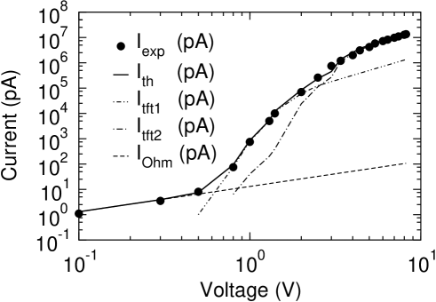
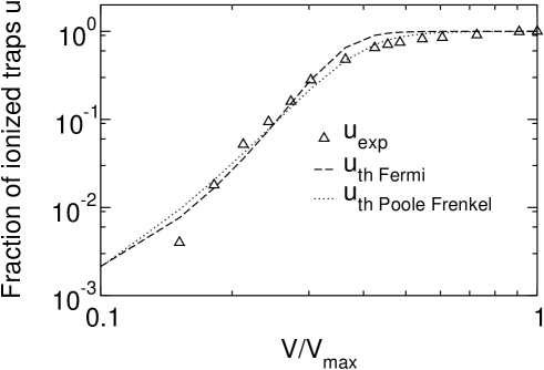
Figures 1, 2 and Figures 3, 4 report, respectively, the I-V characteristics and the associated fraction of filled traps for the case of two different rectangular samples of tetracene [13]. Data reported in Figs. 1 and 2 refer to a sample width of cross sectional area and length , respectively. In this case, the fitting between theory and experiments is obtained by taking:
| (18) |
| (19) |
| (20) |
which imply , ,
Data reported in Figs. 3 and 4 refer to a sample of cross sectional area and length , respectively. In this case, the fitting betwen theory and experiments is obtained by taking:
| (21) |
| (22) |
which implies , ,
Dashed curves in Fig. 1 and Fig. 3 refer to the theoretical fitting carried out within the model of Sec. 2 for a single trap level with the fraction of filled traps reported in Figs. 2 and 4 for the PF model. In Figs. 2 and 4 symbols refer to the values extracted from the fit of experiments and curves refer to the theoretical results obtained from statistics using a Quasi-Fermi (QF) model or a Poole-Frenkel (PF) model, respectively. We found that QF and PF models give very similar results, with the PF model providing a sligthly better agreement with experiments.
The parameters extracted from the fitting for the tetracene samples are summarized in Table 1.
Figures 5 and 6 report, respectively, the I-V characteritics and the associated fraction of filled traps obtained on a sample of pentacene [19] with and . In this case, the fitting is obtained by taking:
| (23) |
| (24) |
| (25) |
which implies , ,
The continuous curve in Fig. 5 refers to the theoretical fitting carried out within the model of Sec. 2 for a double trap level with the fraction of filled traps reported in Fig. 6. In Figure 6 symbols refer to the values extracted from the fit of experiments and curves refer to the theoretical results obtained from statistics using a QF model or a PF model, respectively. Even in this case, we found that QF and PF models give very similar results, with the PF model providing a sligthly better agreement with experiments.
3.2 Relative excess current-noise
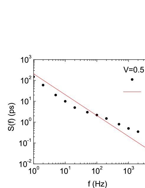
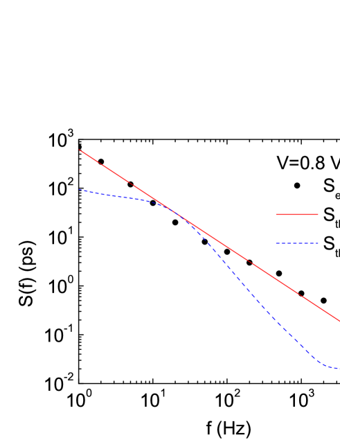
Here we consider the relative excess-noise characteristics measured in tetracene and pentacene samples of [19]. For the case of tetracene, Ref. [17] already reported the fit of the I-V charateristics and of the relative excess-noise measured at 20 Hz as function of the applied voltage for a Au/Tc/Al sample of length and cross-sectional area of . Below, noise spectra in the measured range of the same tetracene sample are fitted using the frequency expressions at the given voltage given by
| (26) |
| (27) |
for a single lifetime (Lorenzian) model, or
| (28) |
for a supeerposition of relaxation processes describewd by broadened set of lifetimes in the range , so that the broadening factor is well approximated by 1 in the considered frequency region.
| (29) |
Figure 7 reports the fraction of filled traps deermnwd from the fitting of the I-V experiments and that are here used for the fitting of the noise spectra.
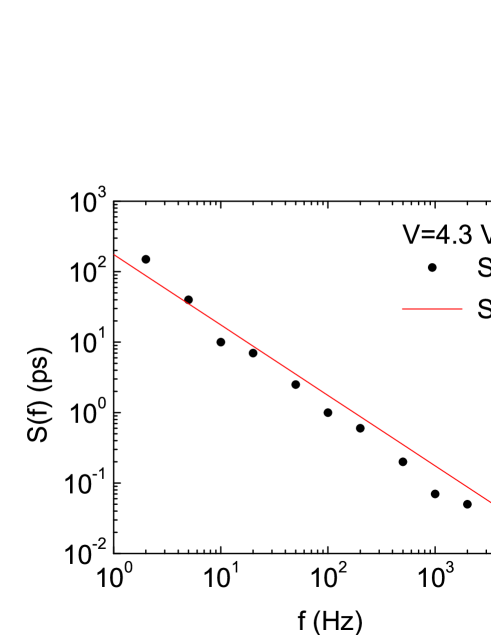
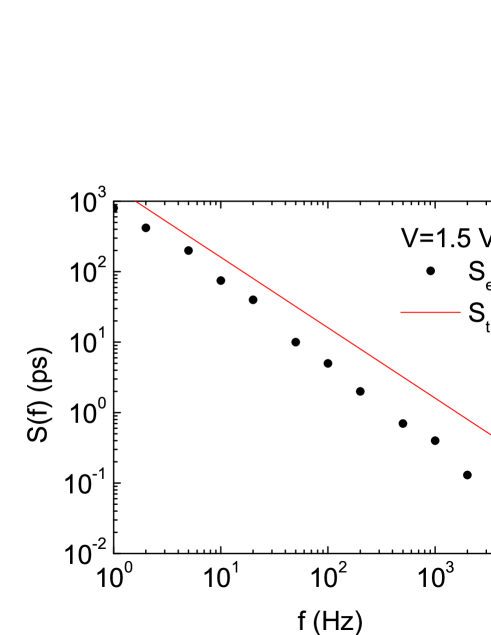
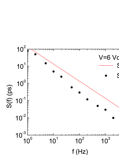
Figures 8 to 12 reports the noise spectra of tetracene [19] for several voltages covering the range from 0.5 to 6 V. We recall that the spectrum at 0.5 V corresponds to the Ohmic regime, spectra at 0.8 and 1.5 V corespond to the TFL regime, and spectra at 4.3 and 6 V correspond to the trap-free SCLC regime. In particular, Fig. 9 at 0.8 V compares the shape of the spectra when going from a single lifetime, , to the broadened set of lifetimes responsible for the 1/f slope. The case of broadened lifetimes well reproduce the like spectra exhibited by experiments in the full frequency range and at voltage regions where the TFT regime is dominant. We notice, that at the highest voltages experiments exhibit a spectra with a slope sligthy sharper than the simple 1/f, and which is responsible of most of the misfit with theory.
For the case of pentacene [19], the theoretical spectra of all the noise source considered are taken to exhibit an 1/f shape and the fitting with experiments is carried out at the frequency of 20 Hz by taking:
| (30) |
| (31) |
| (32) |
| (33) |
| (34) |
The values of the fraction of filled traps obtained from the I-V fit are used as input parameters for the corresponding fit of the relative excess-noise at 20 Hz as function of the applied voltage whivh is reported in Fig. 13. To fix the main parameters of the fitting between theory and experiments we have paralleled the procedure used in [17]. In particular, the maximum value of the trap concentrations and the corresponding estimate of a carrier free-time is obained by solving Eq. (14) for real values of .
The parameters extracted from the fitting of pentacene data are summarized in Table 2.
| Relative dielectric constant | ||
|---|---|---|
| Zero-field hole mobility | ||
| Thermal free-carrier concentration | ||
| Density of traps | ||
| Density of traps | ||
| Valence band state density | ||
| Carriers 1 free time | ||
| Number of carriers 1 | ||
| Carriers 2 free time | ||
| Number of carriers 2 | ||
| Deep trap energy level | ||
| —– | ||
| Trapping factors | ||
| Ohmic Hooge parameter | ||
| SCLC1 Hooge parameter | ||
| SCLC2 Hooge parameter |
Here, in view of the extremely low value of the hole mobility that is estimated from the given geometry, we have considered the possibility that from the electrical point of view the effective area of the contacts be a factor of smaller than the geometrical value reported in experiments [19]. This can happen due to the strong inhomegenety of the organic material that can make only a small fraction of the contact area permeable to the current flow. Accordingly, the corresponding parameters span a comparable range of values (see Table 2).
4 Conclusions
We have developed a phenomenological model that provides a quantitative interpretation of the current-voltage characteristic and the relative excess current-noise in the presence of space-charge limited conditins due to the presence of multiple trapping centers. The model is applied to the case of polyacenes where different sets of experiments are available from literature. We have found an excellent agreement between the predictions of our model and experimental results in tetracene and pentacene thin films of different lemgth in the range . The agreement allows us to state that the sharp peak of noise in the TFT region exhibited by pentacene films arises from the fluctuating occupancy of the traps due to trapping-detrapping processes. The fitting of the I-V and the noise experiments extends over 10 and 4 orders of magnitude, respectively, and provides a set of parameters (see Tables 1 and 2) of valuable interest for the characterization of the samples under investigation.
Finally, we remark that the measured current noise spectrum in the voltage region controlled by the TFT was usually found to be -like [25, 26, 27, 19, 28, 29, 30, 31, 32], thus without a direct evidence of a Lorentzian spectrum, as assumed in Eq. (14). As a consequence, a broadening of the trap lifetimes in the range is considered to account for the shape of the noise spectra [33, 34, 35].
References
- [1] M. Muccini, Nature Materials 5, 605 (2006).
- [2] A. Fleissner H. Schmid, C. Melzer, and H. Seggern, Appl. Phys. Lett. 91, 242103 (2007).
- [3] C.Y. Chen Y. -C. Chao, H. -F. Meng, and S. -F. Horng, Appl. Phys. Lett. 93, 223301 (2008).
- [4] F. Lezzi, G. Ferrari, C. Pennetta, and D. Pisignano, Nano Lett., 15, 7245 (2015)-
- [5] Y. Song, T. Lee, Journal of Materials Chemistry C, (2017).
- [6] D.V- Lang, X. Chi, T. Siegrist, A. M. Sergent, and A. P. Ramirez, Phys. Rev. Lett. 93, 076601 (2004).
- [7] T. Miyadera, S.D. Wang, T. Minari, K. Tsukagoshi, and Y. Aoyagi Appl. Phys. Lett. 93, 033304 (2008).
- [8] N. Koch, A. Elschner, R. L. Johnson, and J. P. Rabe Appl. Surf. Sci. 244, 593 (2005).
- [9] Y.S. Yang, S.H. Kim, J.I. Lee, H.Y. Chu, L.M. Do, H. Lee, J. Oh, and T. Zyung, Appl. Phys. Lett. 80, 1595 (2002).
- [10] D. Knipp, R.A. Street, and A.R. Volkel Appl. Phys. Lett. 82, 3907 (2003).
- [11] F. Dinelli, M. Murgia, P. Levy, M. Cavallini, and F. Biscarini Phys. Rev. Lett. 92, 116802 (2004).
- [12] C.H. Schwalb, S. Sachs, M. Marks, A. Schöll, F. Reinert, E. Umbach, and U. Höfer Phys. Rev. Lett. 101, 146801 (2008).
- [13] R.W.I. De Boer, M. Jochemsen, T.M. Klapwijk, A.F. Morpurgo, J. Niemax, A.K. Tripathi, and J. Pflaum J. Appl. Phys. 95, 1196 (2004).
- [14] J.H.D. Kang Appl. Phys. Lett. 86, 152115 (2005).
- [15] W. Chandra, L.K. Ang, and K.L. Pey, Appl. Phys. Lett. 90, 153505 (2007).
- [16] M. Giulianini, E.R. Waclawik, J.B. Bell, and N. Motta, Appl. Phys. Lett. 94, 083302 (2009). and I. Torres, D.M. Taylor, and E. Itoh, Appl. Phys. Lett. 85, 314 (2004).
- [17] A. Carbone, C. Pennetta and L.Reggiani, Appl. Phys. Lett. 95, 233303 (2009).
- [18] O.D. Jurchescu, B.H. Hamadani, H.D. Xiong, S.K. Park, S. Subramanian, N.M. Zimmerman, J.E. Anthony, T.N. Jackson, and D. J. Gundlach Appl. Phys. Lett. 92, 132103 (2008).
- [19] A. Carbone, B.K. Kotowska, and D. Kotowski, Phys. Rev. Lett. 95, 236601 (2005); and A. Carbone, B K. Kotowska, and D. Kotowski Eur. Phys. J. B 50, 77 (2006).
- [20] Y. Song, H. Jeong, S. Chung, G.H. Ahn, T.Y. Kim, Sci. Rep. 6 33967 (2016).
- [21] M.A. Lampert and P. Mark, Current Injection in Solids, Academic Press, New York (1970).
- [22] J.L. Hartke, J. Appl. Phys. 39, 4871 (1968).
- [23] F.N. Hooge, Phys. Lett. A 29, 139 (1969).
- [24] A. Van der Ziel, Noise: sources, charactrization, measurements, Prentice-Hall, New York (1970).
- [25] P. V. Necliudov, S. L. Rumyantsev, M. S. Shur, D. J. Gundlach and T. N. Jackson J. Appl. Phys. 88, 5395 (2000).
- [26] S. Martin, A. Dodabalapur, Z. Bao, B. Crone, H. E. Katz, W. Li, A. Passner, and J. A. Rogers J. Appl. Phys. 87, 3381 (2000).
- [27] L. K. J. Vandamme, R. Feyaerts, Gy. Trefán, and C. Detcheverry J. Appl. Phys. 91, 719 (2002).
- [28] Lin Ke, Surani Bin Dolmanan, Lu Shen, Chellappan Vijila, Soo Jin Chua, Rui-Qi Png, Perq-Jon Chia, Lay-Lay Chua, and Peter K.-H. Ho J. Appl. Phys. 104, 124502 (2008).
- [29] Hongki Kang, Lakshmi Jagannathan, and Vivek Subramanian Appl. Phys. Lett. 99, 062106 (2011).
- [30] Yong Xu, Takeo Minari, Kazuhito Tsukagoshi, Jan Chroboczek, Francis Balestra, Gerard Ghibaudo, Solid-State Electr. 61 106–110 (2011).
- [31] Rishav Harsh, and K. S. Narayan J. Appl. Phys. 118, 205502 (2015).
- [32] G. Giusi, E. Sarnelli, M. Barra, A. Cassinese, G. Scandurra, K. Nakayama and C. Ciofi, IEEE IEMDC (2017), in press
- [33] T.G.M. Kleinpenning, Physica 94B, 141 (1978); F.N. Hooge, T.G.M. Kleinpenning, and L.K.J. Vandamme, Rep. Prog. Phys. 44, 479 (1981).
- [34] C. Pennetta, E. Alfinito, and L. Reggiani, J. Stat. Mech. p02053 (2009).
- [35] D.M. Fleetwood, IEEE Trans. Nucl. Science, 52, 1462 (2015).