Band dependence of charge density wave in quasi-one-dimensional \ceTa_2NiSe_7 probed by orbital magnetoresistance
Abstract
\ceTa2NiSe7 is a quasi-one-dimensional (quasi-1D) transition-metal chalcogenide with Ta and Ni chain structure. An incommensurate charge-density wave (CDW) in this quasi-1D structure was well studied previously using tunnelling spectrum, X-ray and electron diffraction, whereas its transport property and the relation to the underlying electronic states remain to be explored. Here we report our results of magnetoresistance (MR) on \ceTa2NiSe7. A breakdown of the Kohler’s rule is found upon entering the CDW state. Concomitantly, a clear change of curvature in the field dependence of MR is observed. We show that the curvature change is well described by two-band orbital MR, with the hole density being strongly suppressed in the CDW state, indicating that the orbitals from Se atoms dominate the change in transport through the CDW transition.
Low-dimensional transition-metal chalcogenides (TMC) garnered great interests due to their rich physical properties Wang2012 ; Wang2015 , including the recent discovery of valley dependent transport Mak2012 and superconductivity Lu2015 in MoS2, extremely large MR in WTe2 Ali2014 and the stunning topological phases Qi2011 . The low dimensionality and high structural symmetry makes TMC ideal for studying the structure-property relation. Uniquely, the electron-electron interaction in 1D metals causes strong perturbations, in sharp contrast to the case in the 2D and 3D Fermi-liquid counter parts, and leads to Luttinger liquid (LL) behavior Luttinger1963 . On the other hand, CDW in the quasi-1D metal can be viewed as a classical analogue of a LL state Slot2004 . These facts raise special interests in the study of CDW in 1D metallic systems for exploring emergent behaviours. In addition, strong nonlinear electrical transport due to CDW sliding in 1D chain systems leads to high dielectric constants Zant1996 and narrow-band noise Zybtsev2009 , both of which may find interesting use in applications.
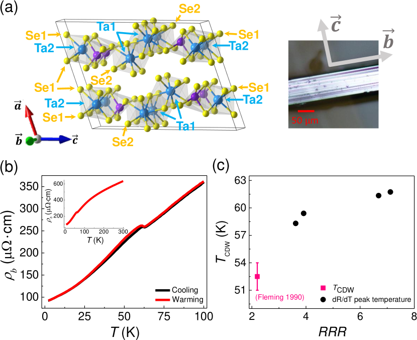
Ta2NiSe7 is a quasi-1D ternary TMC showing an incommensurate CDW Fleming1990 . Its quasi-1D structure is illustrated in Fig. 1(a). Similar to \ceFeNb_3Se_10 Meerschaut1981 , the unit cell of \ceTa2NiSe7 consists of double rows of tantalum atoms (Ta1) in bicapped trigonal prismatic selenium coordination, and the other double rows of tantalum atoms (Ta2) in octahedral selenium coordination; nickel atoms are in highly distorted octahedral coordination. Band structure calculations showed that the Fermi surface consists of contribution from Ta2 orbitals in the octahedral chains and Se2 orbitals from trigonal prismatic columns Canadell1987 . At around 52 K, an incommensurate CDW occurs. Interestingly, the CDW formation mechanism was suggested not to be the Fermi surface nesting effect, but rather, through the charge transfer between the two Ta2 chains STM1992 . However, X-ray diffraction experiment pointed out that all Ta2 atoms are equivalent in symmetry in the CDW stateXray1995 . So far, this discrepancy is not fully resolved, but is mitigated by the observation of two independent CDWs, with modulation wave vector and , each corresponding to the transverse displacement of Ni and Se2 Xray1995 , and the longitudinal modulation of Ta2 Ludecke2000 , respectively.
The CDW in \ceTa2NiSe7 is found to be sensitive to defects Fleming1990 ; Ludecke2000Nb . The typical role of defects on CDW includes scattering carriers, pinning the CDW domains and jeopardising the formation of long-range structural order. In 1D systems, the situation can be more complicated. The spacial distribution of defects can be driven by the CDW order to show a spacial distribution with the same modulation wave vector, which is the so-called defect quasiregularity induced by CDW Baldea1993 . The consequence, such as the thermal hysteresis of the CDW transition Baldea1990 , was indeed found in \ceTa2NiSe7 Fleming1990 . CDW gap only removes part of the Fermi surface, so that the system remains semimetallic below CDW transition temperature () Canadell1987 ; STM1992 .
Regarding the transport property of \ceTa2NiSe7, so far only a small kink in the temperature dependence of resistivity was found to correspond to the CDW Fleming1990 . The transport related to the 1D character, and the underlying electronic states are not explored. Here, we report the result of MR measurement on high-quality \ceTa2NiSe7 single crystals. In addition to a sizable MR up to at low temperatures, we find that the Kohler’s scaling is valid at high temperatures but fails in the CDW state. A clear change of curvature in the field dependence of MR upon entering the CDW state is also observed. The behavior is well interpreted using a two-band orbital MR model, which shows that the hole density is strongly suppressed in the CDW state, while the electron density is less affected. Our results provide transport evidences showing that CDW occurs mostly in hole-like band from Se orbitals.
Ta2NiSe7 single crystals were prepared by flux method. X-ray diffraction (XRD) were performed in Bruker D8 diffractometer. XRD on selected samples showed a space group of , and lattice constants of , , , , , consistent with earlier report Sunshine1986 . Single crystal morphology and elemental analysis were carried out by scanning electron microscope and energy dispersive X-ray spectroscopy. Crystals used in our measurement are highly selected, with a residual resistance ratio , which is the highest among those reported in literature. Typical size of the crystal is . , the resistance along the axis, was measured by standard four terminal method in a Quantum Design PPMS system with a 14 Tesla magnet, with a rotator for controlling the relative orientation between magnetic field and crystal.

Ta2NiSe7 shows a metallic behavior in the temperature range of 2 to 300 K, as shown in Fig. 1(b). , defined by the peak temperature in d/d, is at around 62.5 K. This value is nearly 10 K higher than the 52.5 K reported in earlier literatures Fleming1990 ; STM1992 ; Xray1995 and comparable to the highest reported so far Ludecke2000Nb . The large difference in is attributed to different sample qualities due to the existence of impurities. Typically, this can be characterised using . We studied several samples grown in different batches and obtained the relation between and in Fig. 1(c). The value from an earlier study Fleming1990 is also included in the plot. It is clear to see that increase monotonically with increasing . In this paper, we focus on the sample with the highest of 62.5 K, which corresponds to the lowest impurity concentration. Another interesting feature in is the hysteresis loop below . One should note that the resistivity upon warming is higher than that upon cooling. This feature was attributed to the defect quasi regularity induced by CDW, as described above.


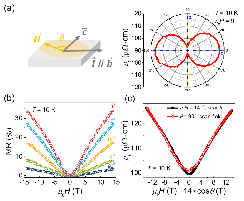
Now we focus on the MR of \ceTa2NiSe7. Shown in Fig. 2 are the MR measured along the axis under a rotating magnetic field in the plane. The polar plot of in Fig. 2(a), measured at 10 K under a 9 T field, shows a pronounced two-fold symmetry, with symmetry axis along / direction. In this configuration, different part of the Fermi surface is probed when the magnetic field rotates along different directions. To explore the nature of the MR at low temperatures, the field dependence of MR at 10 K is shown in Fig. 2(b). MR is largest with field perpendicular to the current (), reaching 35% at 14 T, and decreases progressively to below 4% when the field is parallel to the current. Clearly the orbital MR (also know as the ordinary MR) is dominating. We further illustrate this point in Fig. 2(c) by comparing two curves: for field along axis and under a rotating field of 14 T. For the latter, is essentially the field component perpendicular to the current direction. The two curves overlap rather well, meaning that the field perpendicular to current is critical, which further proves that the effect is dominated by orbital MR. For large region in curve, the field is oriented close to the axis, which in turn probe a different area of Fermi surface, as shown in Fig. 2(a). This leads naturally to the difference between the two curves in the large region (small field region in curve).
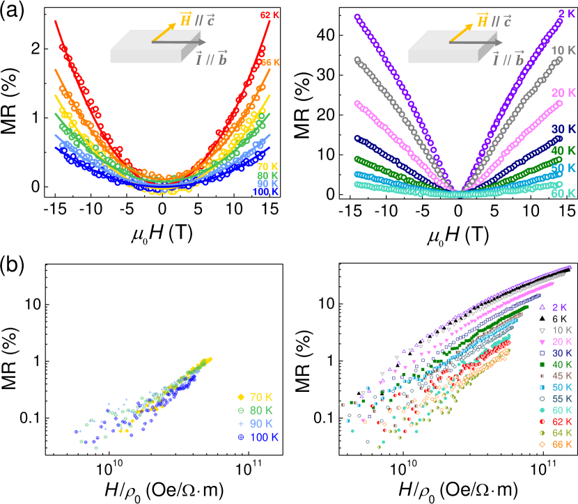
In an in-plane magnetic field perpendicular to current, the field dependence of MR at different temperatures is shown in Fig. 3(a). One major observation is that MR shows concave and convex curvature for temperatures above and below , respectively. The slope change in the field dependence of ordinary MR signifies a multiband effect, consist with the semimetallic band structure found in earlier calculation Canadell1987 . At high temperatures MR features a parabolic field dependence, again indicating that orbital MR is dominating, a mechanism the same with that at low temperatures.
We find that MR data above follows the Kohler’s rule Ziman1972 , namely, . Here is the zero-field resistivity at a given temperature, and stands for a function of . The Kohler’s rule typically holds well for materials with carrier density insensitive to temperature and with isotropic scattering. In Fig. 3(b), data in \ceTa2NiSe7 for falls on a master curve of Kohler scaling, with an exponent of 1.99, as expected for an orbital MR. However, when the temperature is lowered through , significant deviation develops, leading to the scattered curves in the Kohler’s plot, as shown in the right panel of Fig. 3(b). In this multi-band system, the breakdown of Kohler’s rule in the CDW states indicate that either the ratio of electron and hole carrier changes strongly, or the scattering becomes anisotropic. While both possibilities may be relevant, the former appears to be more tempting since a direct consequence of a CDW order is the removal of carriers.

Here we attempt to provide a more quantitative understanding of the MR using the semiclassical two-band resistivity,
Here, is the electron charge, and are the electron and hole density, and are the electron and hole mobility, respectively. With this equation, we can fit the MR at different temperatures and extract the transport quantities. Unfortunately, because of the inclusion of four parameters, it is difficult to get a reliable fitting if we set all the four parameters independent. Now with the implication of the above discussions, especially the clue we obtained in the Kohler scaling, we intentionally set the mobility of electron and hole to be identical to facilitate an easier fitting. Fig. 4(a) shows the representative MR data and the fitting curve. One can see that the two-band ordinary MR equation describes the data quite well, for temperatures both above and below . The resultant fitting parameters are summarized in Fig. 4(b). One will also note that electron and hole are entirely symmetric in the two-band resistivity model, therefore it is impossible to differentiate the two solely from the model. For this we rely on the Hall resistivity data of \ceTa2NiSe7, and found that the hole dominates over the entire temperature range (data not shown here), which allows us to distinguish and in Fig. 4(b). Consistently the resultant hole density is several times higher than the electron density over the entire temperature range. We see that the carrier density shows clearly different behavior for electron-like and hole-like bands: the electron density increases only slightly upon cooling, while the hole density decreases significantly when entering the CDW state. This contrasting behavior shows unambiguously that the CDW gap open predominately in the hole-like band. Recall that the Fermi surface of \ceTa2NiSe7 consists of an electron-like band from Ta2 orbitals in the octahedral chains, and a hole-like band Se2 orbitals from trigonal prismatic columns Canadell1987 , our results indicate that the carrier transport is dominated by hole-like band from the orbitals from Se2 atoms, which finds good consistency with earlier synchrotron X-ray diffraction result that the primary part of CDW resides on Se2 and Ni Xray1995 .
In summary, we report our magneto resistivity measurement on the quasi-1D transition-metal chalcogenide \ceTa2NiSe7. The Kohler’s rule is valid at high temperatures, but breaks down in the CDW state. A clear change of curvature in the field dependence of magnetoresistivity upon entering the CDW state is observed, which is fully accounted for by a two-band ordinary magnetoresistivity model. The two-band fitting shows that the hole carrier density is strongly suppressed in the CDW state, indicating that CDW takes place in hole-like band, mostly the orbitals from Se2 atoms.
The work at SJTU is supported by MOST (Grant No. 2015CB921104) and NSFC (Grant Nos. 91421304 and 11474198), at Penn State by NSF (Grant No. EFMA1433378), at Tulane supported by the U.S. Department of Energy under EPSCoR Grant No. DE-SC0012432 with additional support from the Louisiana Board of Regents (support for a graduate student, materials, travel to NHMFL).
References
- (1) Q. H. Wang, K. Kalantar-Zadeh, A. Kis, J. N. Coleman, and M. S. Strano, “Electronics and optoelectronics of two-dimensional transition metal dichalcogenides,” Nat Nano 7, 699–712 (2012).
- (2) H. Wang, H. Yuan, S. Sae Hong, Y. Li, and Y. Cui, “Physical and chemical tuning of two-dimensional transition metal dichalco-genides,” Chem. Soc. Rev. 44, 2664–2680 (2015).
- (3) K. F. Mak, K. He, J. Shan, and T. F. Heinz, “Control of valley polarization in monolayer MoS2 by optical helicity,” Nat Nano 7, 494–498 (2012).
- (4) J. M. Lu, O. Zheliuk, I. Leermakers, N. F. Q. Yuan, U. Zeitler, K. T. Law, and J. T. Ye, “Evidence for two-dimensional Ising superconductivity in gated MoS2,” Science 350, 1353–1357 (2015).
- (5) M. N. Ali, J. Xiong, S. Flynn, J. Tao, Q. D. Gibson, L. M. Schoop, T. Liang, N. Haldolaarachchige, M. Hirschberger, N. P. Ong, and R. J. Cava, “Large, non-saturating magnetoresistance in WTe2,” Nature 514, 205 (2014).
- (6) X.-L. Qi and S.-C. Zhang, “Topological insulators and superconductors,” Rev. Mod. Phys. 83, 1057–1110 (2011).
- (7) J. M. Luttinger, “An Exactly Soluble Model of a Many‐Fermion System,” Journal of Mathematical Physics 4, 1154–1162 (1963).
- (8) E. Slot, M. A. Holst, H. S. J. van der Zant, and S. V. Zaitsev-Zotov,“One-Dimensional Conduction in Charge-Density-Wave Nanowires,”Phys. Rev. Lett. 93, 176602 (2004).
- (9) H. S. J. van der Zant and O. C. Mantel and C. Dekker and J. E. Mooij and C. Træholt,“Thin‐film growth of the charge‐density‐wave oxide Rb0.30MoO3,”Applied Physics Letters 68, 3823–3825 (1996).
- (10) S. G. Zybtsev, V. Y. Pokrovskii, V. F. Nasretdinova, and S. V. Zaitsev-Zotov,“Gigahertz-range synchronization at room temperature and other features of charge-density wave transport in the quasi-one-dimensional conductor NbS3,”Applied Physics Letters 94, 152112 (2009).
- (11) R. M. Fleming, S. A. Sunshine, C. H. Chen, L. F. Schneemeyer,and J. V. Waszczak,“Defect-inhibited incommensurate distortion in Ta2NiSe7,”Physical Review B 42, 4954 (1990).
- (12) A. Meerschaut, P. Gressier, L. Guemas, and J. Rouxel,“Structural determination of a new one-dimensional niobium chalcogenide: FeNb3Se10,”Materials Research Bulletin 16, 1035–1040 (1981).
- (13) E. Canadell and M. H. Whangbo,“Metallic versus nonmetallic properties of ternary chalcogenides: tantalum metal selenide, Ta2MSe7 (M= nickel, platinum), and tantalum nickel chalcogenide, Ta2NiX5 (X= sulfide, selenide),”Inorganic Chemistry 26, 3974–3976 (1987).
- (14) Z. Dai, C. G. Slough, W. W. McNairy, and R. V. Coleman,“Charge-density-wave formation in Ta2NiSe7 studied by scanning tunneling microscopy,”Physical review letters 69, 1769–1772 (1992).
- (15) A. Spijkerman, A. Meetsma, J. L. de Boer, Y. Gao, and S. van Smaalen,“Modulated structure of NiTa 2 Se 7 in its incommensurate charge-density-wave state at 16 K,”Physical Review B 52, 3892 (1995).
- (16) J. Lüdecke, M. Schneider, and S. van Smaalen,“Independent q→ and 2q→ Distortions in the Incommensurately Modulated Low-Temperature Structure of NiTa2Se7,”Journal of Solid State Chemistry 153, 152 – 157 (2000).
- (17) J. Lüdecke, E. Riedl, M. Dierl, K. Hosseini, and S. van Smaalen,“Influence of niobium on the charge-density-wave transition of ,”Phys. Rev. B 62, 7057–7062 (2000).
- (18) I. Bâldea and M. Bădescu,“Quasiregular impurity distribution driven by a charge-density wave,”Phys. Rev. B 48, 8619–8628 (1993).
- (19) I. Bâldea,“Reentrant charge-density wave in the one-dimensional system with impurities - a self-consistent approach,”Physica Scripta 42, 749 (1990).
- (20) S. A. Sunshine and J. A. Ibers,“Synthesis, structure, and transport properties of tantalum nickel selenide (Ta2NiSe7) and tantalum platinum selenide (Ta2PtSe7),”Inorganic Chemistry 25, 4355–4358 (1986).
- (21) J. Ziman,Principles of the Theory of Solids (Cambridge University Press, 1972).