Large Tunneling Anisotropic Magnetoresistance mediated by Surface States
Abstract
We investigated the tunneling anisotropic magnetoresistance (TAMR) in thick hcp Co films at cryogenic temperatures using scanning tunneling microscopy. At around , a strong TAMR up to 30% is found with a characteristic voltage dependence and a reversal of sign. With the help of ab initio calculations the TAMR can be traced back to a spin-polarized occupied surface states that experience a strong spin-orbit interaction leading to a magnetization direction depending hybridization with bulk states.
Due to its potential for magnetic storage application, the tunneling anisotropic magnetoresistance (TAMR) effect has attracted a lot of attention since its discovery Bode et al. (2002); Gould et al. (2004); Rüster et al. (2005); Giddings et al. (2005); Saito et al. (2005); Giraud et al. (2005). It is cuased by changes in the tunneling density of state (DOS) upon magnetization direction in heterostructures such as ferromagnet/insulator/normal metal junctions. It originates from the spin-orbit coupling (SOC), which lifts the degeneracy of electronic states of a system depending on the magnetization axis. In the case of an out-of-plane TAMR, the magnetic electrode with a magnetization in-plane and out-of-plane exhibits two distinct tunneling DOS Matos-Abiague and Fabian (2009). It can be produced by the Bychkov-Rashba/Dresselhaus SOC field Bychkov and Rashba (1984); Dresselhaus (1955); Matos-Abiague and Fabian (2009) or by a change of the electronic DOS due to SOC induced band splitting Bode et al. (2002). The TAMR effect was reported for a large diversity of magnetic films. For example, diluted magnetic semiconductors such as GaMnAs Gould et al. (2004); Rüster et al. (2005); Giddings et al. (2005); Saito et al. (2005); Giraud et al. (2005) display a sizable TAMR. Due to the lack of inversion symmetry in its Zink-Blend crystalline structure, the Dresselhaus effect combined with the Bychkov-Rashba effect at the interfaces produces a TAMR of the order of a few percent. Electronic states of magnetic 3d metals hybridized with those of 5d transition metals at interfaces (Fe/W Bode et al. (2002), Co/Pt Park et al. (2008); Shick et al. (2006)) constitute a second class of material where TAMR effects up to 10% were reported. Recently, a sizable TAMR effect of 10 % was reported for a simple fcc Co film epitaxially grown on a sapphire substrate without the help of 3d/5d interfaces Wang et al. (2013). In this case, the uniaxial epitaxial strain induces a SOC in combination with a Bychkov-Rashba effect and causes a large TAMR Matos-Abiague et al. (2009).
In order to further increase the TAMR, it was theoretically proposed to use the enhanced SOC in spin-polarized surface state at metallic surfaces and interfaces Chantis et al. (2007); Khan et al. (2008). Indeed, due to the large potential gradient, the Rashba effect can increase at surfaces and interfaces and can strongly affect the electronic band structure. Depending on the magnetization direction, surface states can hybridize with bulk states and give rise to surface resonances that can produce a sizable TAMR. A TAMR of 20% was theoretically predicted in a Fe/vacuum/Cu junction Chantis et al. (2007). Later a similar proposition was given for Fe/MgO/Fe magnetic tunnel junctions Khan et al. (2008), where spin-polarized interface resonances are present Tusche et al. (2005); Tiusan et al. (2004). The advantage of this approach is the strong momentum selectivity of tunneling across the MgO barrier that can reduce the number of states contributing to tunneling. The experimental observation, however, revealed a TAMR of only 1 percent in the Fe/MgO/Fe junctions Lu et al. (2012).
In this Letter, we report record TAMR effects in hcp Co films of the order of 30% without the need of heavy elements. It is caused by magnetization direction dependent hybridization of spin-polarized surface states with bulk bands. We argue that this effect is due to the bulk band structure of Co and as a consequence shows up in many Co film systems suitable for application.
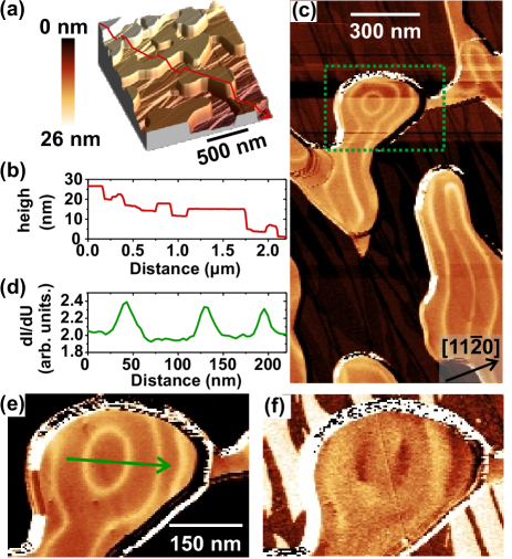
Co films were grown by molecular beam epitaxy from high purity Co rods onto clean Ru(0001) surfaces. Details on the substrate preparation can be found elsewhere Hervé et al. (2018). After deposition of 10 monolayers (ML), the sample was annealed to 450∘C, which leads to partial de-wetting of the film and the formation of flat islands typically about 30 ML local thickness Yu et al. (2002). Fig. 1a shows a typical topographic STM image of the surface. The line scan (Fig. 1b) displays a general tilt of the surface due to an unavoidable miscut of the Ru substrate. The Co islands, however, locally form atomically flat terraces. As it has been reported before, Co grows in its hcp modification on Ru(0001) El Gabali et al. (2007).
Fig. 1c shows a large area map of the differential conductance of the sample taken with a non-magnetic W tip at a bias voltage . A strong contrast is found between the thick hcp Co islands (bright) and the remaining thin wetting layer (dark) due to large difference of their electronic structure. Further a clear contrast can be resolved on the Co islands. On the islands, white lines are found that either are closed loops or end at the edges of the islands. Applying an out-of-plane magnetic field leads to a movement of these white lines (see Supplementary) identifying them as magnetic domain walls. Cobalt in its hcp modification displays a strong uniaxial magnetic anisotropy of about 60% of the dipolar energy with an easy axis along the c-axis of the hcp cell Hubert and Schäfer (1998). Thus, the Co film in this thickness range forms a magnetic stipe domain pattern Hubert and Schäfer (1998), in which the out-of-plane magnetocrystalline anisotropy orients the local magnetization normal to the surface plane, i.e. the magnetization points out-of or into the plane of the surface. The islands split into magnetic domains in the form of a stripe domain pattern in order to reduce the dipolar energy Hubert and Schäfer (1998). Fig. 1d shows a line scan across a zoomed part of the sample displayed in Fig. 1e. As can be seen, the signal on neighboring domains is identical and only the domain walls appear as bright. This excludes that the observed signal is caused by the tunneling magnetoresistance effect, in agreement with the non-magnetic tip. Thus, the signal does not depend on the sign of the magnetization but only on its orientation, i.e. out-of-plane (dark) on the domains and in-plane (bright) on the domain walls. It thus is in accord with a TAMR signal. When dipping the W tip into a thick Co island, magnetic Co can be transferred to the tip and the differential conductance then becomes sensitive to the relative orientation of the local sample magnetization and the tip magnetization due to the tunneling magnetoresistance (TMR) effect Jul (1975); Wiesendanger (2009). As illustrated in Fig. 1f, this changes the observed contrast considerably. In this case, the tip became sensitive to an in-plane component of the sample magnetization and the signal of the domain walls depends on the in-plane direction of the local magnetization. They either appear as bright or dark lines, depending on the direction of magnetization in the walls. Most likely, the walls are of Bloch type due to the large Co thickness Hubert and Schäfer (1998).
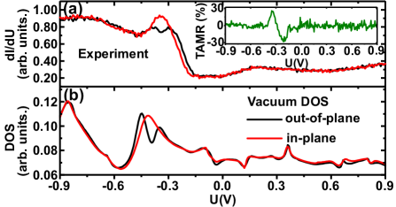
Since the TAMR effect is evoked by spin-orbit interaction causing modifications in the DOS upon changes in the magnetization axis, it is usually very dependent on the bias voltage. In order to study the bias dependence, we recorded the differential conductance on stripe domains with magnetization out-of the plane and domain walls with an in-plane magnetization as function of the bias voltage. Fig. 2a shows the result in a wide voltage range between -900 and . At most bias voltages, is within the noise identical on the differently oriented magnetic structures. Clear differences only appear near , where on the domain walls, a broad peak is observed (red curve) while on the domains, a double peak structure with a local minimum at that voltage is seen (black curve). Note that at this bias voltage, a van Hofe singularity of an occupied minority surface state of Co has been reported for bulk Co and thin Co films Himpsel and Eastman (1979); Diekhöner et al. (2003); Barral et al. (2005); Heinrich et al. (2010). The inset of the Figure shows the TAMR, i.e. the difference of the two signals over the out-of plane signal (green curve), which quantifies the TAMR effect. It clearly shows a resonance behavior around with a dip slightly below and a peak, above. The TAMR is surprisingly large with up to 30%. Note that a similar TAMR is even seen on a single ML of Co on Ru(0001), but with a lower amplitude Hervé et al. (2018).
In order to understand the origin of the TAMR, we carried out first-principles calculations using a full potential relativistic Green function method, specially designed for semi-infinite systems such as surfaces and interfaces Lüders et al. (2001); Geilhufe et al. (2015). The calculations were performed within the density functional theory in a generalized gradient approximation Perdew et al. (1996). signals were simulated within the Tersoff-Hamann approximation, in which a signal is associated with the local density of states (LDOS) calculated in vacuum at a certain distance from the surface Tersoff and Hamann (1985). In our study we calculated the LDOS at from the surface.
The calculated LDOS (Fig. 2b) reproduces the measured signal qualitatively. The overall shape of the LDOS agrees with the experimental data. Especially, it shows nearly identical LDOS for both magnetic configurations at most of the energies, i.e. an absence of a TAMR effect. Only near , the LDOS significantly depends on the orientation axis of the magnetization. The calculated LDOS nicely reflects the single peak structure for in-plane magnetization (red) and the double peak structure for out-of plane magnetization (black). Note that the calculations show a slightly larger difference than observed in the experiment and also the energies are slightly different. These small deviations from the experiment may either be due to the limits of DFT or due to the difference of the samples. In the experiments, we deal with Co films of final thickness on Ru(0001), which may display some strain due to the lattice mismatch to the substrate, while the calculations were carried out for a half-infinite Co structure with its natural lattice constant.
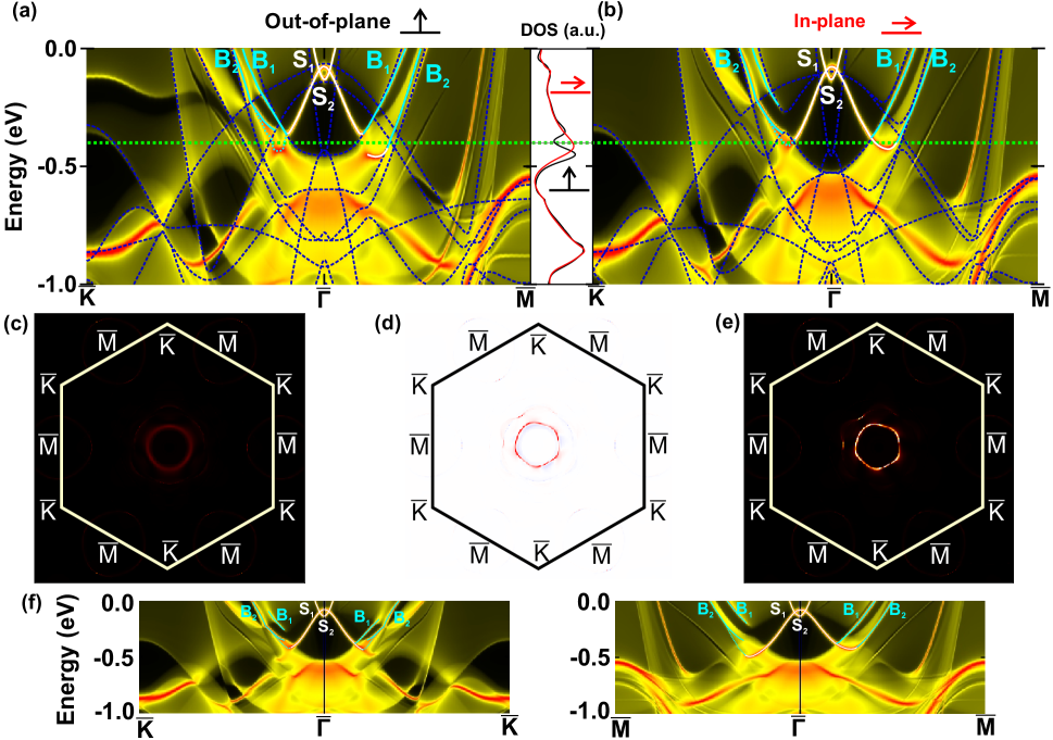
Finally, the DFT calculations allow to identify the origin of the observed large TAMR effect. Fig. 3a and c display the calculated two-dimensional band structure at the Co surface. Bulk states are superposed as dark blue dashed lines while states only present at the surface are displayed in yellow/red. The intensity in the figure represents the weight of the states in a log-scale. For clarity, the surface and surface/bulk hybridized states discussed in the following are marked by white and light blue line respectively. For comparison, the LDOS of Fig. 2b is replotted vertically to size next to the band structure. As can be seen, the difference in LDOS around are caused by large changes in the surface band structure and are related to a forbidden band crossing. In the following, we analyze the band structure in more detail. As can be seen from Fig. 3a) and b), the unoccupied surface state of positive effective mass near the -point is not affected by changes of the magnetization axis and is not involved in the TAMR. Several of the bulk bands, which cross in case of an out-of-plane magnetization, develop forbidden crossings upon rotating the magnetization into the plane. This, however, hardly affects the LDOS of the bulk (see Supplementary). The most prominent changes in the surface electronic structure arises from changes in the surface state . The surface state of negative effective mass is of minority and character Wiebe et al. (2004); Barral et al. (2005); Heinrich et al. (2010). For an in-plane magnetization, merges continuously with the bulk sp-band of positive effective mass causing states with vanishing group velocity and a van Hofe singularity near -400 meV. Figure 3e displays a two-dimensional plot of the states in the surface Brillouin zone and shows a bright ring at that energy as a consequence (plotted on a linear scale). For an out-of-plane magnetization, hybridizes with and develops a gap near -400meV reducing the density of states in the two-dimensional Brillouin zone at that energy (compare Fig. 3c). This gap is responsible for the reduction of the DOS at -400 meV and causes the TAMR. Its spectral weight is shifted away from the gap and causes the double peak feature in the DOS. This is further illustrated by the change of the DOS depicted in Fig.3d plotted in a linear scale (red for reduction an blue for an increase). For clarity, also cuts through the band structure along non-equivalent directions are shown in Fig. 3f for an in-plane magnetization. While for an out-of-plane magnetization, the states at and are equivalent (), for an in-plane magnetization the bands experience a slight shift due to the spin-momentum locking () and direction dependent hybridization with the bulk sp-bands.
In conclusion, we have shown that simple hcp Co shows a large TAMR of 30% near caused by surface states. Thus, this effect is expected to be rather robust to the details of the Co film. Note that similar surface states have been reported even for 2 ML Co films on Cu(111) and Au(111) of both fcc and hcp stacking Heinrich et al. (2010) and Co on W(110) Wiebe et al. (2004). As shown recently, a similar contrast was even found for a single ML of Co on Ru(0001) Hervé et al. (2018), further emphasizing the robustness of this effect.
We acknowledge funding by the Deutsche Forschungsgemeinschaft (DFG) under the grant WU349/15-1, by the European Commission (Grant ATOMS FP7/2007-2013-62260), discussions with B. Dupé and M. Martins, and technical support from J. Chen, M. Peter and J. Jandke.
References
- Bode et al. (2002) M. Bode, S. Heinze, A. Kubetzka, O. Pietzsch, X. Nie, G. Bihlmayer, S. Blügel, and R. Wiesendanger, Phys. Rev. Lett. 89, 237205 (2002).
- Gould et al. (2004) C. Gould, C. Rüster, T. Jungwirth, E. Girgis, G. M. Schott, R. Giraud, K. Brunner, G. Schmidt, and L. W. Molenkamp, Phys. Rev. Lett. 93, 117203 (2004).
- Rüster et al. (2005) C. Rüster, C. Gould, T. Jungwirth, J. Sinova, G. M. Schott, R. Giraud, K. Brunner, G. Schmidt, and L. W. Molenkamp, Phys. Rev. Lett. 94, 027203 (2005).
- Giddings et al. (2005) A. D. Giddings, M. N. Khalid, T. Jungwirth, J. Wunderlich, S. Yasin, R. P. Campion, K. W. Edmonds, J. Sinova, K. Ito, K.-Y. Wang, et al., Phys. Rev. Lett. 94, 127202 (2005).
- Saito et al. (2005) H. Saito, S. Yuasa, and K. Ando, Phys. Rev. Lett. 95, 086604 (2005).
- Giraud et al. (2005) R. Giraud, M. Gryglas, L. Thevenard, A. Lemaître, and G. Faini, Applied Physics Letters 87, 242505 (2005).
- Matos-Abiague and Fabian (2009) A. Matos-Abiague and J. Fabian, Phys. Rev. B 79, 155303 (2009).
- Bychkov and Rashba (1984) Y. A. Bychkov and E. I. Rashba, Journal of Physics C: Solid State Physics 17, 6039 (1984).
- Dresselhaus (1955) G. Dresselhaus, Phys. Rev. 100, 580 (1955).
- Park et al. (2008) B. G. Park, J. Wunderlich, D. A. Williams, S. J. Joo, K. Y. Jung, K. H. Shin, K. Olejník, A. B. Shick, and T. Jungwirth, Phys. Rev. Lett. 100, 087204 (2008).
- Shick et al. (2006) A. B. Shick, F. Máca, J. Mašek, and T. Jungwirth, Phys. Rev. B 73, 024418 (2006).
- Wang et al. (2013) K. Wang, T. L. A. Tran, P. Brinks, J. G. M. Sanderink, T. Bolhuis, W. G. van der Wiel, and M. P. de Jong, Phys. Rev. B 88, 054407 (2013).
- Matos-Abiague et al. (2009) A. Matos-Abiague, M. Gmitra, and J. Fabian, Phys. Rev. B 80, 045312 (2009).
- Chantis et al. (2007) A. N. Chantis, K. D. Belashchenko, E. Y. Tsymbal, and M. van Schilfgaarde, Phys. Rev. Lett. 98, 046601 (2007).
- Khan et al. (2008) M. N. Khan, J. Henk, and P. Bruno, Journal of Physics: Condensed Matter 20, 155208 (2008).
- Tusche et al. (2005) C. Tusche, H. L. Meyerheim, N. Jedrecy, G. Renaud, A. Ernst, J. Henk, P. Bruno, and J. Kirschner, Phys. Rev. Lett. 95, 176101 (2005).
- Tiusan et al. (2004) C. Tiusan, J. Faure-Vincent, C. Bellouard, M. Hehn, E. Jouguelet, and A. Schuhl, Phys. Rev. Lett. 93, 106602 (2004).
- Lu et al. (2012) Y. Lu, H.-X. Yang, C. Tiusan, M. Hehn, M. Chshiev, A. Duluard, B. Kierren, G. Lengaigne, D. Lacour, C. Bellouard, et al., Phys. Rev. B 86, 184420 (2012).
- Hervé et al. (2018) M. Hervé, B. Dupé, R. Lopes, Böttcher, M. Martins, T. Balashov, L. Gerhard, J. Sinova, and W. Wulfhekel, Nature Com. accepted (2018).
- Yu et al. (2002) C. Yu, J. Pearson, and D. Li, Journal of Applied Physics 91, 6955 (2002).
- El Gabali et al. (2007) F. El Gabali, J. Puerta, C. Klein, A. Saa, A. Schmid, K. McCarty, J. Cerda, and J. de la Figuera, New J. of Phys. 9, 80 (2007).
- Hubert and Schäfer (1998) A. Hubert and R. Schäfer, Springer (1998).
- Jul (1975) Physics Letters A 54, 225 (1975), ISSN 0375-9601.
- Wiesendanger (2009) R. Wiesendanger, Rev. Mod. Phys. 81, 1495 (2009).
- Himpsel and Eastman (1979) F. Himpsel and D. Eastman, Phys. Rev. B 20, 3217 (1979).
- Diekhöner et al. (2003) L. Diekhöner, M. Schneider, A. Baranov, V. Stepanyuk, P. Bruno, and K. Kern, Phys. Rev. Lett. 90, 236801 (2003).
- Barral et al. (2005) M. Barral, M. Weissmann, and A. Llois, Phys. Rev. B 72, 125433 (2005).
- Heinrich et al. (2010) B. Heinrich, C. Iacovita, M. Rastei, L. Limot, V. Ignatiev, P.A. ans Stepanyunk, and J. Bucher, Eur. Phys. J. B. 75, 49 (2010).
- Lüders et al. (2001) M. Lüders, A. Ernst, W. M. Temmerman, Z. Szotek, and P. J. Durham, Journal of Physics: Condensed Matter 13, 8587 (2001).
- Geilhufe et al. (2015) M. Geilhufe, S. Achilles, M. A. Köbis, M. Arnold, I. Mertig, W. Hergert, and A. Ernst, Journal of Physics: Condensed Matter 27, 435202 (2015).
- Perdew et al. (1996) J. P. Perdew, K. Burke, and M. Ernzerhof, Phys. Rev. Lett. 77, 3865 (1996).
- Tersoff and Hamann (1985) J. Tersoff and D. R. Hamann, Phys. Rev. B 31, 805 (1985).
- Wiebe et al. (2004) J. Wiebe, L. Sacharow, A. Wachowiak, G. Bihlmayer, S. Heinze, S. Blügel, M. Morgenstern, and R. Wiesendanger, Phys. Rev. B 70, 035404 (2004).