Supercurrent through a spin-split quasi-ballistic point contact in an InAs nanowire
Abstract
We study the superconducting proximity effect in an InAs nanowire contacted by Ta-based superconducting electrodes. Using local bottom gates, we control the potential landscape along the nanowire, tuning its conductance to a quasi-ballistic regime. At high magnetic field (), we observe approximately quantized conductance plateaus associated with the first two spin-polarized one-dimensional modes. For T, the onset of superconductivity occurs in concomitance with the development of sizeable charge localization leading to a 0.7-type conductance anomaly. In this regime, the proximity supercurrent exhibits an unusual, non-monotonic dependence. We interpret this finding in terms of a competition between the Kondo effect, dominating near , and the Zeeman effect, enforcing spin polarization and the emergence of a phase shift in the Josephson relation at higher .
One-dimensional (1D) semiconductor nanowires (NWs) with strong spin-orbit coupling and induced superconductivity are attracting considerable attention owing to their potential to realize topological superconductivity and emergent Majorana modes Lutchyn et al. (2010); Oreg et al. (2010); Lutchyn et al. (2017); Aguado (2017). For a topological phase to be established, the 1D character has to be preserved over micron-scale lengths and the chemical potential needs to be positioned within the so-called helical gap opened by a properly oriented magnetic field Chen et al. (2017). Given the modest size of the spin-orbit energy 111of the order of eV according to tight-binding atomistic and self-consistent simulation of the band structure of an InAs nanowire of diameter = 20 nm (Zaiping Zeng and Yann-Michel Niquet, private communication). See also, Ref. Nadj-Perge et al. (2012)., the second condition implies that the 1D conduction mode supporting Majoranas should be only slightly filled. For this reason, it is important to explore the 1D properties of semiconductor NWs at low subband filling, in the presence of the superconducting proximity effect and an externally applied magnetic field. To this aim, we investigate InAs NWs in combination with tantalum-based superconducting contacts with a high in-plane critical magnetic field, .
Conductance quantization is the most commonly observed experimental signature of ballistic 1D transport Van Wees et al. (1988). In semiconductor NWs, this phenomenon is more easily observed at large magnetic field Weperen et al. (2013), where backscattering is reduced and spin degeneracy is simultaneously lifted, leading to conductance steps of , where is the electron charge and the Planck constant. More recently, conductance quantization was observed also at zero magnetic field, with steps of due to two-fold spin degeneracy Heedt et al. (2016); Kammhuber et al. (2016); Zhang et al. (2017); Fadaly et al. (2017); Gooth et al. (2017); Estrada Saldaña et al. (2017). Here we make use of two independently tunable bottom gates in order to tailor the potential landscape in the NW channel Estrada Saldaña et al. (2017). Proper tuning of the applied gate voltages results in the creation of a local point contact exhibiting approximately quantized conductance plateaus in the few-channel regime. Interestingly, we find that unintentional charge localization, while seemingly suppressed at high magnetic field, becomes apparent at low field, resulting in a 0.7-type conductance anomaly, a phenomenon largely studied in quantum point contacts formed within high-mobility two-dimensional heterostructures Cronenwett et al. (2002); Thomas et al. (1996); Sfigakis et al. (2008); Iqbal et al. (2013) and only recently in NWs Heedt et al. (2016).
In this exotic regime, and thanks to the large electron g-factor in InAs and to the relatively large , we are able to investigate the superconducting proximity effect coexisting with a strong -field-induced spin polarization. We observe a non-monotonic behavior of the critical current as a function of field that can be understood as a Zeeman-driven quantum phase transition from a spin singlet ground state, with 0-phase-shift Josephson coupling, to a spin-1/2 ground state, with -phase-shift Josephson coupling. Upon increasing the magnetic field, the supercurrent first vanishes at the - transition, and then recovers once the Zeeman energy is large enough to stabilize the spin-1/2 ground state, resulting in a non-monotonic dependence. This interpretation is confirmed by theoretical calculations based on an Anderson-type model coupled to superconducting leads with strong and gate-dependent tunnel couplings.
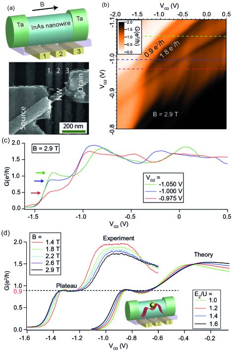
The device designed for our experiment is shown in Fig. 1a. It was fabricated from a single, 65-nm-diameter InAs NW grown by chemical beam epitaxy Gomes et al. (2015). The NW was deposited on a bed of narrow gate electrodes covered by 12 nm of HfO2. Successively, Ta (60 nm)/Al (15 nm) source and drain contacts with a spacing of 280 nm were defined by e-beam lithography and subsequent e-beam evaporation. The latter was preceded by a gentle in-situ Ar etching to remove the native oxide of the NW. The Ta/Al contacts were measured to be superconducting below a critical temperature, K, which is consistent with values reported for Ta in the crystalline -phase ( K Schwartz et al. (1972)). The sample was mounted in a dilution refrigerator (base temperature of 15 mK), and a magnetic field, , was applied in the device plane using a vector magnet. In all of the measurements presented here, was aligned with the longitudinal axis of the NW (data for different angles can be found in the Supplementary Material).
In order to look for conductance quantization, the device was first brought to the normal state by applying a high magnetic field B = 2.9 T, i.e. well above ; the linear conductance, , was measured as a function of voltages and , applied to gates 2 and 3, respectively (Fig. 1b). Two conductance plateaus, around and , can be identified, i.e. close to the ideally expected values for one and two 1D modes and , respectively. As we shall see further below, these modes are resulting from the Zeeman-induced splitting of the first spin-degenerate 1D subband.
To a closer look, Fig. 1b shows noticeable structures consisting of conductance modulations of up to 20% superimposed on the quantized plateaus. We ascribe these modulations to tunneling resonances associated mainly with quasi-localized states in the quantum point contact. Such states are expected to have similar capacitive coupling to gates 2 and 3, hence producing the predominantly diagonal conductance ridges observed in Fig. 1b. The amplitude of these additional features varies over the (,) plane and can vanish at certain regions.
Figure 1c shows three traces taken at different as indicated by the horizontal dashed lines in Fig. 1b. The green trace exhibits a clearly visible broad peak structure causing an overshoot of the conductance at the onset of the first plateau. This structure is no longer present in the blue trace resulting in an essentially flat conductance plateau. Further increasing results in a global suppression of the conductance step (red trace).
From now on we focus our attention on the intermediate value of , where the first conductance step is “cured” from spurious resonances thereby resembling the one expected for the onset of the first 1D conduction mode in a ballistic point contact. From a comparison with the other traces we know that a resonance is in fact lurking in this seemingly ideal conductance plateau. This underlines the importance of double gate control in revealing the nature of the observed transport features. The underlying presence of charge localization is on the other hand apparent in the second plateau where conductance oscillations remain clearly visible (Fig. 1c 222We note that the second plateau extends on a much larger range suggesting that conductance is limited by the barrier induced by .).
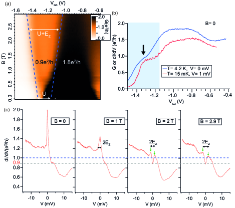
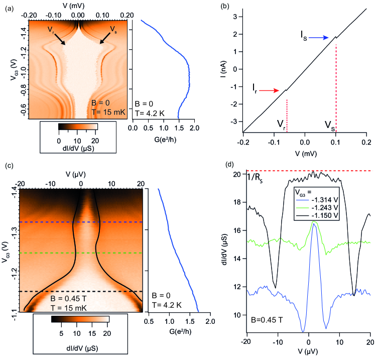
The first conductance plateau preserves its flat, featureless character over a relatively large magnetic field range. Upon reducing down to 1.4 T (Fig. 1d), the plateau shrinks with due to the decreasing Zeeman energy, , with being the Bohr magneton and the electron g-factor in the point contact, while the conductance remains quantized at . Below 1.4 T, a conductance enhancement begins to emerge due to supercurrents (not shown). The full-range B-field dependence is shown as a color-scale plot in Fig. 2a.
The superimposed dashed lines highlight the -evolution of the first conductance plateau. Interestingly, the two lines do not coalesce at as we may expect if the width of the plateau were proportional to . Instead, a residual zero-field splitting remains. Its origin can be ascribed once again to a localized charge state, most likely the evolution to zero field of the one already identified at T. The residual splitting is indicative of a sizable charging energy ( meV with 333Converting the scale into energy is possible with the help of differential conductance () measurements at finite source-drain bias voltage, . This standard procedure (Supplementary Material) yields a conversion factor = 0.0082 meV/mV) associated with the localized state.
Localized states are often observed in semiconductor NWs. They can form Weis et al. (2014); Schroer and Petta (2010); Voisin et al. (2014) due to a plethora of confining mechanisms: crystal defects or impurities in the NW, tunnel barriers at the contacts, surface charges, or Friedel oscillations in electron density. In a gate-defined point contact, where charge density is substantially lowered and electric-field screening consequently reduced, localization is enhanced and Coulomb interaction emerges. Strongly localized states leading to a few rather sharp Coulomb resonances can indeed be observed in the studied gate-induced constriction near full charge depletion. They lie at further negative gate voltages, outside the (, ) field explored in Fig. 1b (see Supplementary Material). The localized state at the onset of the first conductance plateau has a more subtle nature, and, as we have seen, its presence may go unperceived without a proper control of the electrostatic landscape.
At , transport is largely affected by the superconducting proximity effect. A dissipation-less supercurrent sets in already at the onset of the first quasi-ballistic conduction mode leading to a divergence of the conductance. Before discussing the superconducting regime it is instructive to examine the normal type behavior, which can be accessed at temperatures above . Figure 2b shows a characteristic measurement at 4.2 K. Interestingly, the onset of conduction through the first spin-degenerate subband (whose conductance is around 1.5 , i.e. somewhat lower than at B = 2.9 T) is preceded by a shoulder at . A shoulder can also be consistently found in a measurement of at and = 15 mK, where is the superconducting gap.
This feature is reminiscent of a phenomenon known as the ”0.7 anomaly”, largely studied in conventional quantum point contacts Van Wees et al. (1988) electrostatically defined in a high-mobility two-dimensional electron gas . The origin of the 0.7 anomaly has received a variety of explanations raising a long-standing debate Micolich (2011). A number of works point toward Kondo-effect physics associated with a localized state in the QPC Cronenwett et al. (2002); Heyder et al. (2015); Brun et al. (2016); Meir et al. (2002), a physical picture that, in view of the already discussed observations, appears be appropriate to the system studied here. This picture is further confirmed by measurements for different values of and fixed at the shoulder. The data, plotted in Fig. 2c, show the characteristic Zeeman splitting of a zero-bias Kondo resonance. At , the resonance has a zero-bias divergence due to the superconducting proximity effect.
To confirm our interpretation in terms of a quasi-ballistic QPC with a 0.7-type anomaly arising from a localized spin-1/2 state, we model the device using the following Anderson-type Hamiltonian:
| (1) |
Here is the localised level occupancy operator, its energy position (later we shall scale to for a direct comparison with the experimental data) and its spin operator. The coupling between the level and the leads, , results in a broadening , where is the density of states in the leads. The operator quantity corresponds to a correlated-hopping term introducing a perturbation of the level hybridization whose magnitude depends on its occupation for opposite spins Meir et al. (2002). We find that = -0.4 yields the best agreement with the data. We assume to depend quadratically on (and hence on ) and through the relation . The dependence can be expected from the influence of the magnetic field on the orbital motion and confinement of electrons. The last term in Eq. (1) accounts for superconducting pairing, with being the induced superconducting gap.
The model was solved using the numerical renormalization group (NRG) method Wilson (1975); Bulla et al. (2008).
We begin by applying the model to the normal regime () at high . We find that the free parameters of the model are severely constrained even if only qualitative features of the conductance are to be reproduced for different and . In this sense, the model is robust. At , Kondo correlations at finite enhance the conductance to a value below the unitary limit producing a 0.7-type conductance shoulder at , as experimentally observed at K (Fig. 2b). At finite , the shoulder evolves into a plateau at . The results of the NRG calculations reproduce remarkably well the experimental trend as shown in Fig. 1d. In particular, the calculated conductance at the spin-resolved 0.7 anomaly remains constant despite the large variation of the ratio. The -dependent term (proportional to ), even if small against the gate dependent term (proportional to ), is essential to produce this behavior. Without it, the plateau would evolve into a local minimum, as we actually find experimentally when is applied perpendicularly to the NW under the same gate configuration (see Supplementary Material).
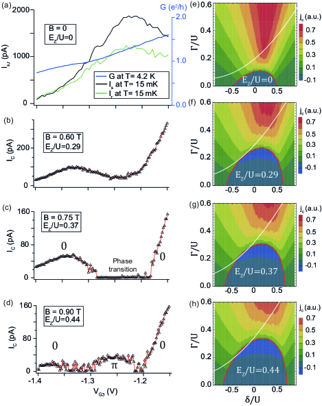
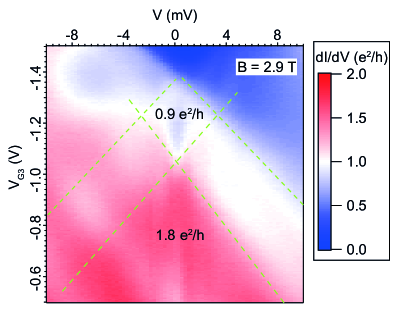
We are now ready to address the superconducting proximity effect in the 0.7-anomaly regime. Figs. 3a-d show supercurrent measurements as a function at different values of . Except for panel a, showing switching and re-trapping currents directly measured at , the other panels display traces obtained from fitting to the so-called resistively and capacitively shunted junction (RCSJ) model (details on the measurement and fitting methodology are given in the Supplementary Material). Remarkably, while the normal conductance increases monotonically with (see the superimposed trace in panel a), does not, in contrast to the Ambegaokar-Baratoff relation, for which . At , the switching currents (closely related to ) are slightly peaked in correspondence with the 0.7-anomaly regime. Upon increasing , develops a minimum around (panel g) and gets fully suppressed for T (panel h) before re-emerging at higher (panel i).
The above behavior can be explained using the Hamiltonian in Eq. (1). Figs. 3e-h show NRG calculations of , as a function of and . We used meV, as deduced from tunnel spectroscopy measurements close to full channel depletion (see Supplementary Material). The plots depict phase diagrams consisting of an open region where (corresponding to a spin-singlet ground state) and a closed region where (corresponding to a spin-1/2 ground state). The sign reversal reflects a phase shift in the current-phase Josephson relation.
Due to the positive sign of the parameter, the phase boundary has the shape of a skewed arc leaning to the right. The case (Fig. 3e) has been extensively studied both theoretically Meng et al. (2009) and experimentally Cleuziou et al. (2006); Van Dam et al. (2006); Jörgensen et al. (2007); Eichler et al. (2009); Maurand et al. (2012); Delagrange et al. (2017); Lee et al. (2017). In the odd-charge regime (), strong (weak) coupling tends to stabilize a singlet (doublet) ground state. The singlet has a predominantly BCS character for , and a predominatly Kondo character for . The Zeeman effect contrasts both of these many-body phenomena thereby reducing the singlet binding energy and making the spin-1/2 domain grow (Figs. 3f-h) Lee et al. (2014).
The above phase diagrams can account for the unusual, non-monotonic dependence of observed experimentally. The white lines in Figs. 3e-h denote the trajectory followed in the experimental sweeps, as deduced from normal-state fit parameters. As the doublet region of the phase diagram grows with , its phase boundary approaches the trajectory leading to a suppression of in the region of closest proximity. At , the phase boundary reaches the trajectory and is correspondingly fully suppressed due to a competition between 0- and -junction behavior. For larger , the trajectory crosses the spin-1/2 region within which the system acquires a clear -junction behavior characterized by the emergence of a negative .
In conclusion, we have shown that, even when seemingly absent, charge localization may play a crucial role in the transport properties of semiconductor NWs. The herein employed multi-gate device geometry proved to be essential towards clarifying this behavior. We have further shown that charge localization in a NW junction gives rise to a strong non-monotonic behavior of the Josephson current as a function of due to 0.7 physics. Our findings own relevance also in relation to experiments aiming at detecting Majorana modes in Josephson junction geometries based on depleted NWs under strong Zeeman fields Tiira et al. (2017); Gharavi et al. (2017); Zuo et al. (2017). In particular, the predictions based on the anomalous B-field dependence of the critical current owing to the presence of Majoranas in the junction San-Jose et al. (2014); Cayao et al. (2017); San-Jose et al. (2013) may be masked by the localization effects and the 0.7 physics discussed here.
We acknowledge financial support from the Agence Nationale de la Recherche, through the TOPONANO project, and from the EU through the ERC grant No. 280043. R. A. acknowledges financial support from the Spanish Ministry of Economy and Competitiveness through Grant FIS2015-64654-P. R. Ž. acknowledges the support of the Slovenian Research Agency (ARRS) under Program P1-0044 and J1-7259.
References
- Lutchyn et al. (2010) R. M. Lutchyn, J. D. Sau, and S. D. Sarma, Phys. Rev. Lett. 105, 077001 (2010).
- Oreg et al. (2010) Y. Oreg, G. Refael, and F. Von Oppen, Phys. Rev. Lett. 105, 1 (2010), 1003.1145 .
- Lutchyn et al. (2017) R. M. Lutchyn, E. P. A. M. Bakkers, L. P. Kouwenhoven, P. Krogstrup, C. M. Marcus, and Y. Oreg, arXiv:1707.04899 (2017).
- Aguado (2017) R. Aguado, Riv. Nuovo Cimento 40, 523 (2017).
- Chen et al. (2017) J. Chen, P. Yu, J. Stenger, M. Hocevar, D. Car, S. R. Plissard, E. P. Bakkers, T. D. Stanescu, and S. M. Frolov, Science advances 3, e1701476 (2017).
- Note (1) Of the order of eV according to tight-binding atomistic and self-consistent simulation of the band structure of an InAs nanowire of diameter = 20 nm (Zaiping Zeng and Yann-Michel Niquet, private communication). See also, Ref. Nadj-Perge et al. (2012).
- Van Wees et al. (1988) B. J. Van Wees, H. Van Houten, C. W. J. Beenakker, J. G. Williamson, L. P. Kouwenhoven, D. Van Der Marel, and C. T. Foxon, Phys. Rev. Lett. 60, 848 (1988).
- Weperen et al. (2013) I. V. Weperen, S. R. Plissard, E. P. A. M. Bakkers, S. M. Frolov, and L. P. Kouwenhoven, Nano Letters 13, 387 (2013).
- Heedt et al. (2016) S. Heedt, W. Prost, J. Schubert, D. Grützmacher, and T. Schäpers, Nano letters 16, 3116 (2016).
- Kammhuber et al. (2016) J. Kammhuber, M. C. Cassidy, H. Zhang, Ö. Gül, F. Pei, M. W. A. de Moor, B. Nijholt, K. Watanabe, T. Taniguchi, D. Car, S. R. Plissard, E. P. A. M. Bakkers, and L. P. Kouwenhoven, Nano letters 16, 3482 (2016).
- Zhang et al. (2017) H. Zhang, Ö. Gül, S. Conesa-Boj, M. P. Nowak, M. Wimmer, K. Zuo, V. Mourik, F. K. de Vries, J. van Veen, M. W. A. de Moor, J. D. S. Bommer, D. J. van Woerkom, D. Car, S. R. Plissard, E. P. A. M. Bakkers, M. Quintero-Pérez, C. M. C., S. Koelling, S. Goswami, K. Watanabe, T. Taniguchi, and L. P. Kouwenhoven, Nature communications 8, 16025 (2017).
- Fadaly et al. (2017) E. M. T. Fadaly, H. Zhang, S. Conesa-Boj, D. Car, Ö. Gül, S. R. Plissard, R. L. M. Op het Veld, S. Kölling, L. P. Kouwenhoven, and E. P. A. M. Bakkers, Nano Letters 17, 6511 (2017).
- Gooth et al. (2017) J. Gooth, M. Borg, H. Schmid, V. Schaller, S. Wirths, K. Moselund, M. Luisier, S. Karg, and H. Riel, Nano Letters 17, 2596 (2017).
- Estrada Saldaña et al. (2017) J. C. Estrada Saldaña, J. P. Cleuziou, E. J. H. Lee, D. Car, S. R. Plissard, E. P. A. M. Bakkers, and S. De Franceschi, arXiv:1709.02614 (2017).
- Cronenwett et al. (2002) S. M. Cronenwett, H. J. Lynch, D. Goldhaber-Gordon, L. P. Kouwenhoven, C. M. Marcus, K. Hirose, N. S. Wingreen, and V. Umansky, Phys. Rev. Lett. 88, 226805 (2002).
- Thomas et al. (1996) K. Thomas, J. Nicholls, M. Simmons, M. Pepper, D. Mace, and D. Ritchie, Phys. Rev. Lett. 77, 135 (1996).
- Sfigakis et al. (2008) F. Sfigakis, C. Ford, M. Pepper, M. Kataoka, D. Ritchie, and M. Simmons, Phys. Rev. Lett. 100, 026807 (2008).
- Iqbal et al. (2013) M. Iqbal, R. Levy, E. Koop, J. Dekker, J. P. de Jong, J. van der Velde, D. Reuter, A. Wieck, R. Aguado, and Y. Meir, Nature 501, 79 (2013).
- Gomes et al. (2015) U. Gomes, D. Ercolani, V. Zannier, F. Beltram, and L. Sorba, Semiconductor Science and Technology 30, 115012 (2015).
- Schwartz et al. (1972) N. Schwartz, W. Reed, P. Polash, and M. H. Read, Thin Solid Films 14, 333 (1972).
- Note (2) We note that the second plateau extends on a much larger range suggesting that conductance is limited by the barrier induced by .
- Note (3) Converting the scale into energy is possible with the help of differential conductance () measurements at finite source-drain bias voltage, . This standard procedure (Supplementary Material) yields a conversion factor = 0.0082 meV/mV.
- Weis et al. (2014) K. Weis, S. Wirths, A. Winden, K. Sladek, H. Hardtdegen, H. Lüth, D. Grützmacher, and T. Schäpers, Nanotechnology 25, 135203 (2014).
- Schroer and Petta (2010) M. Schroer and J. Petta, Nano letters 10, 1618 (2010).
- Voisin et al. (2014) B. Voisin, V.-H. Nguyen, J. Renard, X. Jehl, S. Barraud, F. Triozon, M. Vinet, I. Duchemin, Y.-M. Niquet, S. De Franceschi, and M. Sanquer, Nano letters 14, 2094 (2014).
- Micolich (2011) A. Micolich, Journal of Physics: Condensed Matter 23, 443201 (2011).
- Heyder et al. (2015) J. Heyder, F. Bauer, E. Schubert, D. Borowsky, D. Schuh, W. Wegscheider, J. von Delft, and S. Ludwig, Phys. Rev. B 92, 195401 (2015).
- Brun et al. (2016) B. Brun, F. Martins, S. Faniel, B. Hackens, A. Cavanna, C. Ulysse, A. Ouerghi, U. Gennser, D. Mailly, P. Simon, S. Huant, V. Bayot, M. Sanquer, and H. Sellier, Phys. Rev. Lett. 116, 136801 (2016).
- Meir et al. (2002) Y. Meir, K. Hirose, and N. S. Wingreen, Phys. Rev. Lett. 89, 196802 (2002).
- Wilson (1975) K. G. Wilson, Rev. Mod. Phys. 47, 773 (1975).
- Bulla et al. (2008) R. Bulla, T. A. Costi, and T. Pruschke, Rev. Mod. Phys. 80, 395 (2008).
- Meng et al. (2009) T. Meng, S. Florens, and P. Simon, Phys. Rev. Lett. , 38 (2009).
- Cleuziou et al. (2006) J.-P. Cleuziou, W. Wernsdorfer, V. Bouchiat, T. Ondarçuhu, and M. Monthioux, Nature nanotechnology 1, 53 (2006).
- Van Dam et al. (2006) J. A. Van Dam, Y. V. Nazarov, E. P. Bakkers, S. De Franceschi, and L. P. Kouwenhoven, Nature 442, 667 (2006).
- Jörgensen et al. (2007) H. I. Jörgensen, T. Novotný, K. Grove-Rasmussen, K. Flensberg, and P. E. Lindelof, Nano Letters 7, 2441 (2007).
- Eichler et al. (2009) A. Eichler, R. Deblock, M. Weiss, C. Karrasch, V. Meden, C. Schönenberger, and H. Bouchiat, Phys. Rev. B 79, 2 (2009).
- Maurand et al. (2012) R. Maurand, T. Meng, E. Bonet, S. Florens, L. Marty, and W. Wernsdorfer, Phys. Rev. X 2, 1 (2012).
- Delagrange et al. (2017) R. Delagrange, R. Weil, A. Kasumov, M. Ferrier, H. Bouchiat, and R. Deblock, Physica B: Condensed Matter (2017).
- Lee et al. (2017) E. J. Lee, X. Jiang, R. Aguado, C. M. Lieber, and S. De Franceschi, Phys. Rev. B 95, 180502 (2017).
- Lee et al. (2014) E. J. Lee, X. Jiang, M. Houzet, R. Aguado, C. M. Lieber, and S. De Franceschi, Nature nanotechnology 9, 79 (2014).
- Tiira et al. (2017) J. Tiira, E. Strambini, M. Amado, S. Roddaro, P. San-Jose, R. Aguado, F. S. Bergeret, D. Ercolani, L. Sorba, and F. Giazotto, Nat. Commun. 8, 14984 (2017).
- Gharavi et al. (2017) K. Gharavi, G. W. Holloway, R. R. LaPierre, and J. Baugh, Nanotechnology 28, 085202 (2017).
- Zuo et al. (2017) K. Zuo, V. Mourik, D. B. Szombati, B. Nijholt, D. J. van Woerkom, A. Geresdi, J. Chen, V. P. Ostroukh, A. R. Akhmerov, S. R. Plissard, D. Car, E. P. A. M. Bakkers, D. I. Pikulin, L. P. Kouwenhoven, and S. M. Frolov, Phys. Rev. Lett. 119, 187704 (2017).
- San-Jose et al. (2014) P. San-Jose, E. Prada, and R. Aguado, Phys. Rev. Lett. 112, 137001 (2014).
- Cayao et al. (2017) J. Cayao, P. San-Jose, A. M. Black-Schaffer, R. Aguado, and E. Prada, Phys. Rev. B 96, 205425 (2017).
- San-Jose et al. (2013) P. San-Jose, J. Cayao, E. Prada, and R. Aguado, New J. of Phys. 15, 075019 (2013).
- Nadj-Perge et al. (2012) S. Nadj-Perge, V. Pribiag, J. Van den Berg, K. Zuo, S. Plissard, E. Bakkers, S. Frolov, and L. Kouwenhoven, Phys. Rev. Lett. 108, 166801 (2012).
Supplementary Materials: Supercurrent through a spin-split quasi-ballistic point contact in an InAs nanowire
I Lever-arm parameter
The lever-arm parameter = 0.0082 meV/mV used to convert to energy was extracted from the differential conductance (dI/dV) colormap taken at T shown in Fig. S1.
II Resonances before the conductance plateau
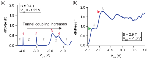
The linear conductance exhibited a few quantum dot resonances at more negative than the region displaying quantized conductance at large field shown in the main text. These resonances are plotted in Fig. S2a, together with the parity of the states (E:even; O:odd). The width of these resonances increases with , corroborating our assumption of a tunnel coupling dependent on this gate. This succession of Coulomb resonances confirms the odd parity of the state whose screening results in the 0.7 anomaly.
III Many-subbands regime
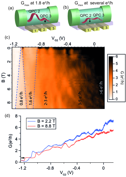
At certain gate configurations, the two barriers of the quantum dot described in the main text could be best described as two quantum point contacts (QPCs) in series. We call them QPC 2 and QPC 3, for their location in the sections of the nanowire above gates 2 and 3, respectively (see the scheme in Fig. S3a).
In the main text, QPC 2 was kept nearly closed at a negative voltage of , which restricted the conductance to values below h, no matter how much we opened QPC 3 by pushing to positive voltage (see Fig. S2b). QPC 2 enforced in this case a one-subband regime.
The ample tunability of our device also allowed us to explore a regime of transport through many subbands, in which case QPC 3 was open and QPC 2 was varied (see the scheme in Fig. S3b). In this new gate configuration, gate 3 was fixed at , and was swept.
Figure S3c shows a measurement of the magnetic field evolution of G in this new configuration as a function of , with the field oriented at 45∘ with respect to the axis of the nanowire. In this plot, blue dashed lines were added to follow the Zeeman splitting of conductance plateaus. Two cuts taken from this plot at (displayed in Figure S3d) show that a clear conductance plateau develops at h, denoting that a QPC regime exists at this gate voltage.
These measurements, together with the ones of the main text, provide a global picture of the way the conduction-band profile of the nanowire can be altered by the two gates, leading either to low-transparency localization, QPC conductance quantization or, remarkably, to a localized magnetic impurity that mimics conductance quantization at large field.
IV Dependence of the linear conductance on the magnetic field when aligned perpendicular to the axis of the nanowire
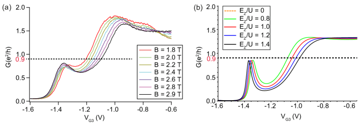
Figure S4a shows the perpendicular magnetic field evolution of G at a field large enough to suppress superconductivity. Instead of a plateau of quantized conductance -as observed for parallel magnetic field under the same conditions (main text)-, there is a peak followed by a dip in the conductance. Furthermore, the conductance in the dip decreases as the magnetic field is increased.
This magnetic field behavior can be qualitatively understood if we assume that the tunnel coupling does not increase with the magnetic field (but just with ), which results in a more pronounced Coulomb blockade effect. Figure S4b shows that, indeed, the NRG model as described in the main text can qualitatively replicate the experimental data of Fig. S4a when, as opposed to the parallel-field case, we neglect the quadratic term arising from the -contribution by setting in (,).
The observation of a conductance plateau for parallel field, and Coulomb blockade oscillations for perpendicular field, confirms once more to the quantum dot nature of the 0.7 anomaly in the device. This is distinctively different from a conventional QPC behavior, where conductance quantization occurs regardless of the field direction, aside from backscattering suppression.
V Equivalent circuit and quality factor of the Josephson junction
The nanowire Josephson junction was underdamped at low magnetic field and/or with low critical current (which happened at low normal-state conductance), and mostly overdamped at high magnetic field. In this section we explain why this is the case.
Figure S5a shows the equivalent circuit of the Josephson junction device. The cold parts of the circuit, which were kept at T15 mK during the measurement, are encircled by dashed lines. The voltage source and the ammeter are at room temperature; the latter in series with a resistance of about 10 k from the current amplifier.
The cold parts of the circuit consisted of a filtering stage (black dashed lines), the on-chip leads (blue dashed lines), and the sample (red dashed lines). The filtering stage had a two-stage RC circuit, with =10 k and =10 nF. Since there are four of these resistances in series with the sample, the total resistance in series with the sample was of about 50 k.
The on-chip leads capacitance was estimated at F from the capacitance of two neighboring bonding pads. The resistance of the leads was determined by fitting of the supercurrent V- characteristic to be R1.6 k, as explained in the next section.
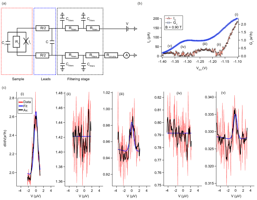
In the circuit of Figure S5a, the sample itself is modeled as a Josephson supercurrent source I() of critical current , in parallel with a junction resistance and a junction capacitance . and depended on the gate voltage and ranged, respectively, from 20 pA to 2 nA, and from 20 k to 100 k. could also depend on the bias voltage , but for the small bias applied on the device at high magnetic field -of less than 20 -, this dependency could be dropped. The value of could be estimated from the charging energy U1.3 meV, from which we obtain F.
In the resistively and capacitively shunted junction (RCSJ) model, the quality factor of the junction can be evaluated by the following formula Jörgensen et al. (2007):
| (S1) |
For our sample, the factor is gate-dependent because and are not inversely proportional to each other for all gate voltages. Since and are also changing with magnetic field, will be a function of the gate voltage and the magnetic field.
Nevertheless, it is possible to roughly estimate for a few values of and and see its tendency. At , at the supercurrent maximum of Figure 3a of the main article and therefore the junction is underdamped for this particular gate voltage. At the supercurrent minimum of the same plot, when the normal conductance of the sample is low, and the junction is slightly overdamped. At this gate voltage, and are equal. Since tends to decrease with a rising magnetic field, becomes smaller as the magnetic field increases, and the junction is predominantly overdamped.
Figures S6a,c show raw-data conductance maps as a function of the gate voltage , at and at T, respectively. In these maps, whenever the supercurrent is non-dissipative, it appears as a plateau of conductance around zero-bias, such as in the black curve in Figure S6d. This plateau, if the junction is underdamped, will be bound by and , which are proportional to the re-trapping () and switching () current. and are indicated in the map of Figure S6a. in most of this gate range, as for an underdamped junction. To extract and , we took V-I curves like the one in Figure S6b, in which these quantities are indicated. In this curve, and are easily distinguishable.
At B = 0.45 T, the junction becomes overdamped for all the gate range shown in the raw data of Figure S6c. This is revealed by the symmetry of the supercurrent with respect to zero bias, if one corrects for a 2 V voltage offset from the voltage source. The magnetic field renders the junction overdamped, consistently with our estimation of Q.
Figure S6d shows three raw conductance traces taken from the map (along the dashed lines of the same color as the corresponding curves). At this magnetic field, the supercurrent is non-dissipative only around the black dashed line, as shown in the black curve, whose conductance approaches . At lower gate voltage, there is a zero-bias peak instead of a plateau, and its conductance is clearly below . Here the supercurrent manifests itself as a dissipative conductance peak, which occurs because the Josephson energy becomes so small that it attains the same order of magnitude as the thermal energy. In the next section, we detail how the critical current was extracted in this case.
VI Method for fitting the supercurrent
The critical current was obtained from a fit of the corrected V - data with the theory derived from the RCSJ model with thermal noise in Ref. Ivanchenko and Zil ’berman (1969), extended in Ref. Ambegaokar and Halperin (1969) and used in Refs. Jörgensen et al. (2007); Eichler et al. (2009); Steinbach et al. (2001). The correction of the voltage and the conductance consisted in subtracting the series resistance according to: and . We assumed, as also done in Refs. Jörgensen et al. (2007); Eichler et al. (2009), that the current-phase relationship was sinusoidal (). This assumption may no longer hold near the singlet doublet transition point Delagrange et al. (2016). Since we took V - measurements, the derivative of the original formula given in equation S2 was taken, where is the modified Bessel function of complex order , , and is the ratio between the Josephson energy and the thermal energy. This equation contains the resistance of the junction , which was added to the original expression given in Ref. Ivanchenko and Zil ’berman (1969) to account for an additional multiple Andreev reflection (MAR) channel in parallel with the Josephson current Jörgensen et al. (2007). The resistance provides an ohmic contribution at a current above the critical current.
| (S2) |
For a small Josephson energy with respect to the thermal energy (i.e., ), which was the case for , the dI/dV expression simplifies to Ivanchenko and Zil ’berman (1969):
| (S3) |
Both equations give similar results for 0.6 T. An example of five fits (i-v) that produce the and data points indicated in the re-emergent supercurrent plot of Figure S5b is given in Figure S5c. As it is seen in this series of plots, the supercurrent arises as a narrow -a few wide- and small zero-bias peak in the conductance. A large supercurrent produces a large zero-bias peak (i) -and viceversa (iii and v). When there is no peak (ii and iv), as it occurs in a phase transition, the critical current is zero or attains a very small value below 20 pA. We fit the data at all magnetic fields studied with and k as fitting parameters.
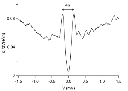
VII Superconducting gap
Fig. S7 shows a plot of the superconducting gap with the nanowire near depletion, in the tunnel regime. meV is extracted from this measurement, in agreement with the of thin Ta films evaporated with a similar procedure as the one used for the contacts of the device. This value was used in the NRG calculations of the supercurrent through the spin-split single level.
VIII NRG calculations
The numerical renormalization group (NRG) calculations for the Hamiltonian [Eq. (1) in the main text] have been performed to determine the normal-state differential conductance (for ) and the Josephson current (for ) in the presence of the magnetic field. For normal-state properties, we used NRG discretization parameter , two interleaved discretization meshes, keeping up to 5000 multiplets (or using an energy cutoff at energy in the units of the characteristic energy scale of a given NRG step). The conductance was extracted from raw dynamical properties data without performing a spectral broadening. The calculations in the superconducting state were performed with , keeping up to 10000 multiplets (or using an energy cutoff at energy ). These calculations were performed for a range of phase difference , from which we extracted the critical current defined as the Josephson current such that the absolute value is maximized.
References
- Jörgensen et al. (2007) H. I. Jörgensen, T. Novotný, K. Grove-Rasmussen, K. Flensberg, and P. E. Lindelof, Nano Letters 7, 2441 (2007).
- Ivanchenko and Zil ’berman (1969) Y. M. Ivanchenko and L. A. Zil ’berman, Soviet Physics Jetp 28, 1272 (1969).
- Ambegaokar and Halperin (1969) V. Ambegaokar and B. I. Halperin, Phys. Rev. Lett. 23, 274 (1969).
- Eichler et al. (2009) A. Eichler, R. Deblock, M. Weiss, C. Karrasch, V. Meden, C. Schönenberger, and H. Bouchiat, Phys. Rev. B 79, 2 (2009).
- Steinbach et al. (2001) A. Steinbach, P. Joyez, A. Cottet, D. Esteve, M. Devoret, M. Huber, and J. M. Martinis, Phys. Rev. Lett. 87, 137003 (2001).
- Delagrange et al. (2016) R. Delagrange, R. Weil, A. Kasumov, M. Ferrier, H. Bouchiat, and R. Deblock, Phys. Rev. B 93, 195437 (2016).