Density and Microstructure of -C Thin Films
Abstract
In this work, we studied amorphous carbon (-C) thin films deposited using direct current (dc) and high power impulse magnetron sputtering (HiPIMS) techniques. The microstructure and electronic properties reveal subtle differences in -C thin films deposited by two techniques. While, films deposited with dcMS have a smooth texture typically found in -C thin films, those deposited with HiPIMS consist of dense hillocks surrounded by a porous microstructure. The density of -C thin films is a decisive parameter to judge their quality. Often, x-ray reflectivity (XRR) has been used to measure the density of carbon thin films. From the present work, we find that determination of density of carbon thin films, specially those with a thickness of few tens of nm, may not be accurate with XRR due to a poor scattering contrast between the film and substrate. By utilizing neutron reflectivity (NR) in the time of flight mode, a technique not commonly used for carbon thin films, we could accurately measure differences in the densities of -C thin films deposited using dcMS and HiPIMS.
I Introduction
Amorphous carbon (-C), graphite and diamond are well-known allotropes of carbon. Graphite with a layered hexagonal crystal structure has sp2 hybridization and in diamond due to a tetrahedral structure, hybridization is sp3. On the other hand, -C is somewhere in between, having a mixture of both hybridizations Robertson (2002). Due to presence of a significant fraction of sp3 hybridization and properties similar to diamond, (-C) is also referred as diamond like carbon (DLC). -C has several interesting properties they are mechanically hard, chemically inert and transparent (mainly in infrared region) Robertson (2002), etc. Therefore, -C films are widely used as protective coatings of magnetic data storage devices, biomedical equipments, optical windows and cold neutron applications. With such an excellent physical, mechanical and chemical properties, it has gained attention among the researcher and in coating technology.
An -C thin film can be deposited using chemical vapor deposition (CVD) or physical vapor deposition (PVD) ( pulse laser deposition (PLD), sputtering) techniques. When deposited using CVD, generally -C thin films have hydrogen(H) contamination. Among the PVD techniques, PLD has been frequently used to deposit -C films having sp3 fraction as high as 80 Gaumet et al. (1993); Yamamoto et al. (1998). On the other hand, it is well-known that small sample size and lower deposition rates limit the uses of PLD for mass production and industrial uses. Another PVD technique that is magnetron sputtering (MS), has also emerged as an industrially accepted technique for preparation of H free -C thin films. Though the sp3 fraction is found to be typically 45 in sputtered film Logothetidis et al. (1999). It may be noted that in a typical direct current MS (dcMS) process, the plasma is dominated by neutrals and the fraction of ions is very small (5). On the onset of this century, an advancement in dcMS was seen in terms of high power impulse magnetron sputtering (HiPIMS). In HiPIMS very large power (about 103 greater than that in dcMS) may enhance the fraction of ions to the extent that it can be even larger than neutral atoms. HiPIMS technique was immediately applied for preparation of thin films of transition metal compounds e.g. TiO2 Konstantinidis et al. (2006), TiN Lattemann et al. (2010), CrN Lin et al. (2011) etc. A general observation in terms of properties of deposited films was observed as the morphology was globular rather than columnar observed in dcMS. Sporadic attempts have also been made to deposit -C films with HiPIMS. However, in most of the studies so far, the characterization of plasma has been the focus, rather than the properties of resulting films Lattemann et al. (2011); Sarakinos et al. (2012); Nakao et al. (2013); Huang et al. (2013); Lin et al. (2014). Lattemann Lattemann et al. (2011) used HiPIMS together with arc mode to find enhancement in C ions and resulting films were found to have graphitic clusters. In another study with rather high frequency (250 Hz to 1 kHz), the plasma was found to have larger ionized species yielding enhance densification with larger sp3 fraction Sarakinos et al. (2012). In more recent, works Ar and C2H2 gas mixture were used to deposit -C films but films were not H free Kimura and Kamata (2016); Aijaz et al. (2016). Clearly, HiPIMS offers possibilities to deposit carbon thin films with high density and high sp3 fractions, and more systematic studies are required to achieve this.
Microstructure and density of -C thin films determines their merit. The microstructure and the electronic structure of -C thin films have been well-established and techniques employed to measure them are: transmission electron microscopy (TEM), atomic force microscopy (AFM), scanning electron microscopy (SEM); and electronic structure using Raman, x-ray photo electron spectroscopy (XPS) and C K-edge x-ray absorption spectroscopy (XAS). In detailed study by Ferrari et al. Ferrari et al. (2000a) it was found that there is near linear dependence of density with sp3 fraction. Therefore density of -C thin films is pivotal to determine their quality. Generally, x-ray reflectivity (XRR) has been the technique used most frequently to measure the density of -C thin films. In most of the studies an -C film has been deposited on a Si substrate. The density of -C (typically 2.2 g/cm3) films is slightly less than that of Si (2.3 g/cm3). In a typical XRR pattern two critical angles are expected Ferrari et al. (2000a). However, their separation is too close to observe experimentally and it may happen that the critical angle of -C film get merged together with Si. In this case, rather than measuring the density of -C film, the density of Si substrate is measured. It may be noted that in recent works though density of -C films have been determined using XRR Lattemann et al. (2011); Sarakinos et al. (2012), either XRR patterns were not shown or the separation of critical edges of C and Si could not be seen Liu et al. (2016). Moreover, as pointed out in a seminal work by Wallace et al. Wallace and Wu (1995), determination of density from typical XRR measurements (angle dispersive - 2 scans) could have errors up to 5 due to sample misalignment and a similar error may get augmented as the critical edge is not well defined due to similarity in densities of C and Si.
It is surprising to note that neutron reflectivity (NR), which is otherwise similar to XRR, has not yet been used to determine the density of -C films. For C and Si, neutron scattering length densities are: 7.3310-6 and 2.0410-6 Å-2; for Cu K x-rays they are: 1.8710-5 and 2.0110-5 Å-2, respectively. Since for neutrons, C is a stronger scatterer, therefore the critical angle is exclusively determined by C. Moreover, by doing NR measurements in energy dispersive or time of flight (TOF) mode, the angle of incidence is kept fixed (no movement of sample during measurement). Therefore foot print effects can be avoided completely and the critical angle of the density of C thin films can be measured much more precisely than XRR. In the present work, we have shown this amply for C thin films deposited using dcMS and HiPIMS techniques. As shown in this work, with XRR small difference in the density of C films could not be probed, they could be seen clearly with NR. In addition synchrotron based C K-edge x-ray absorption spectroscopy (XAS) was used to investigate the nature of bonding and hybridization. Combining XRR, NR and XAS data with laboratory based techniques - AFM and XPS, we probed the microstructure and density of -C thin films.
II Experimental Details
Carbon thin films were deposited using dcMS and HiPIMS at room temperature (without any intentional heating) using a 3 inch C (99.999% purity) target (Orion-8, AJA Int. Inc. system). The base pressure of the chamber was of the order of 1 Torr and working pressure was 3 mTorr due to flow of Ar gas (99.9995% purity) at 20 sccm. It is expected that by using a pure C target, low background pressure and pure Ar gas, the resulting films would be hydrogen free, unlike those obtained by a chemical precoces Weiler et al. (1994). Films were deposited at an average power (current) of 100 W (0.2 A), both for dcMS and HiPIMS process but the peak power (current) obtained in the later was about 28 kW (56 A). Typical deposition times were about 1 h in dcMS and 2 h in the HiPIMS process. The duty cycle used in the HiPIMS process was about 0.35 (pulse length 70 s and frequency 50 Hz). Samples were deposited on a Si(100) substrate and the target to substrate distance was kept fixed at about 12 cm. For better uniformity substrates were continuously rotated around their own axis at 60 rpm. Resulting films were characterized for their thickness, density and roughnesses by x-ray reflectivity (XRR) using a standard diffractometer (Bruker D8 Discover) equipped with a Cu kα x-ray source. To gain further insight about parameters obtained from XRR measurements, we did neutron reflectivity (NR) measurements at AMOR reflectometer in time of flight mode at SINQ/PSI, Switzerland Stahn and Glavic (2016); Gupta et al. (2004). The electronic structure of the samples were determined using x-ray absorption near edge spectroscopy (XANES) technique at the C K-edge in total electron yield (TEY) mode at BL01 beamline at Indus-2 synchrotron radiation source at RRCAT, Indore Phase et al. (2014). We have also used x-ray photoelectron spectroscopy (XPS) to study the electronic structure. The XPS measurement were carried out using Electron Spectroscopy for Chemical Analysis (ESCA) spectrometer equipped with Al kα x-ray source. Both XANES and XPS measurements were performed under UHV conditions. Surface morphology of the deposited samples were determined by atomic force microscopy(AFM) operating in contact mode.
III Results and Discussion
III.1 Atomic Force Microscopy
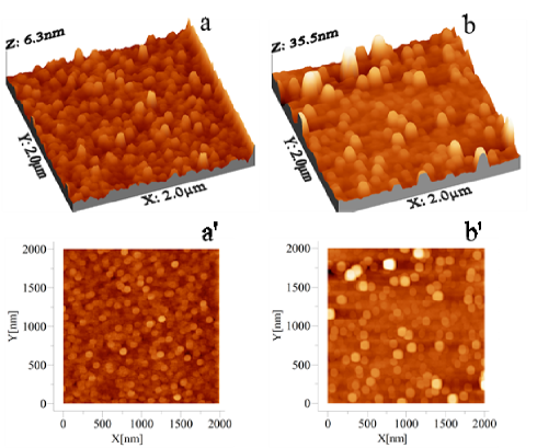
Surface morphologies of the deposited samples obtained from AFM measurements are shown in fig. 1. Images were processed using WSxM software package Horcas et al. (2007). Keeping X and Y scale constant in all images at 22 m2, the Z-scale was varied on the basis of maximum column height. It is about 65 Å for films grown with dcMS (fig. 1 (a), (a′)) and about 350 Å for samples grown with HiPIMS(fig. 1 (b), (b′). As can be seen from AFM images, film grown using HiPIMS has topographical distribution which is about 5 times higher in height than those in dcMS deposited films. This indicates that while films deposited using dcMS are smooth, those deposited using HiPIMS have a distribution in which large columns or hillocks are surrounded by voids. It is known that the density of ions is larger in the HiPIMS process and when deposited film gets bombarded with ions, this could result in such distribution leading to formation of a porus microstructure. The consequences of these are also reflected in the density as well as in the orbital ordering, which is measured with XRR, NR, XPS and C K-edge XANES and presented in next section.
III.2 X-ray and Neutron Reflectivity
XRR is one of the well-known techniques for determining thickness (), roughness () and number density () or mass density of thin films. For x-rays, refractive index (n) is a complex number and it is slightly less than unity, and can be expressed as:
| (1) |
where,
| (2) |
here and are dispersive and absorptive part of the refractive index, is absorption coefficient, is linear absorption coefficient and is classical radii of electron. The x-ray scattering length density (SLD) is frequently used as: (i) Re(SLD)=Z and (ii) Im(SLD)=. Since absorption of x-rays takes place in material, it carries information related to presence of vacancy, defects etc.
| Technique/ | dcMS | HiPIMS | |||||||
|---|---|---|---|---|---|---|---|---|---|
| Parameter | XRR | NR | XRR | NR | |||||
| (5) Å | 251 | 256 | 384 | 391 | |||||
| Re10-5Å-2 | 1.910.01 | 0.660.002 | 1.920.02 | 0.710.005 | |||||
| Im10-8Å-2 | 3.05 | 0 | 33 | 0 | |||||
| g/cm3 | 2.250.01 | 1.980.004 | 2.260.02 | 2.140.005 | |||||
| (2)Å | 6.4 | 8 | 8.0 | 10 |
On the other hand, neutron reflectivity is also a frequently used technique specially for magnetic thin films, as neutrons carries a magnetic moment Ott (2007). In addition, NR has been frequently used for low Z materials and polymers due to large scattering cross-sections for H and D Penfold (2002). In view of this, it is surprising to note that NR has not yet been used to study -C thin films even though the mass density of C and Si is very close. Since neutron scattering takes place from nucleus, and therefore the neutron scattering length () can differ significantly between neighboring elements. For C and Si, is 6.5 fm and 4.15 fm, respectively. Similar to x-rays, the refractive index for neutrons can be written as:
| (3) |
Here is number density and the imaginary term has been omitted as for C and Si it is about six orders of magnitude smaller than dispersive part due to smaller absorption of neutrons.
It may be noted that XRR has been frequently used to study -C films Ferrari et al. (2000b); Patsalas et al. (2005). Generally, -C thin films are deposited on a Si or SiO2 substrate. X-ray scattering contrast between the substrate and C is rather poor due to nearly equal number densities Re(SLD)C = 1.8710-5Å-2 (mass density =2.2 g/cm3) and Re(SLD)Si = 1.9810-5 Å-2 (=2.3 g/cm3). In the study of -C films with XRR, apart from thickness () and roughness (), the density of the film has been often determined. Generally in an angle dispersive XRR measurement typical errors in determination of density are about 5% Wallace and Wu (1995). In addition, due to similar values of Re(SLD) for C and Si, the critical angle is not well defined and determination of density from XRR measurement could easily have another 5% error, signifying that even from a very careful experiment, the density of -C film could have errors exceeding 10%.
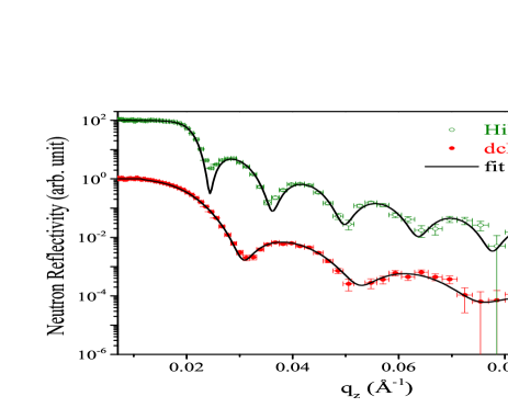
On the other hand, neutron has a large scattering contrast between C and Si due to large differences in their scattering lengths and resulting number densities for neutrons are = 7.3310-6Å-2 and = 2.0410-6 Å-2. In addition, absorption of neutrons is almost negligible unlike x-rays and therefore, number densities can be determined more precisely Wallace and Wu (1995). Moreover, by doing neutron reflectivity measurements in the time of flight (ToF) mode (similar to energy dispersive), the sample is kept at a fixed angle of incidence and therefore illumination remains constant. Hence, foot print effects can be avoided completely and the critical angle is well-defined so that density can be determined more accurately. Our comparison of both XRR and NR, clearly shows the limitation of XRR determination of density specially for carbon thin films.
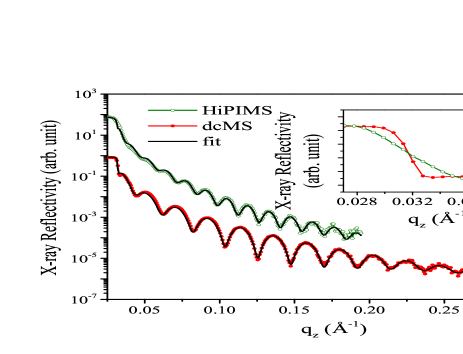
XRR and NR patterns for both samples are shown in fig. 2 and 3, respectively. They were fitted using a Parratt32 software package Parratt (1954) to obtain , and and are shown in table 1. As can be seen there, the value of thickness and roughness obtained from XRR and NR are similar (within experimental errors), as expected. But mass density of films calculated from XRR and NR are at large variance and the value of densities both for dcMS and HiPIMS deposited films are similar at about 2.25 g/cm3. It may be noted that the mass density of Si is about 2.3 g/cm3. Therefore, it may be possible that rather than film, the substrate density is measured. On the other hand, we find that the values of mass densities obtained from NR measurements are 1.98 and 2.14 g/cm3, respectively for dcMS and HiPIMS deposited films. Clearly, films deposited with HiPIMS have larger density and it can only be probed by doing NR measurements in the ToF mode.
An additional feature that can be seen from the XRR pattern is the behavior of critical edges for the samples deposited with dcMS and HiPIMS as shown in the inset of fig. 2). Such behavior can only be fitted taking a much higher value for the imaginary part of SLD. From table 1, we find that the value of ImSLD is about 10 times higher for the film deposited using HiPIMS. Such a significant increase in ImSLD can be understood by analyzing the XPS and XAS results, which are presented in next sections.
III.3 X-ray Photoelectron Spectroscopy
X-ray photoelectron spectroscopy (XPS) is one of the well-known technique to determine sp2 and sp3 fractions in a -C sample. The XPS spectra shown in fig. 4 can be deconvoluted in three components (i) sp2 (ii) sp3 and (iii) C bonded with oxygen, following ref. Ansell et al. (1979). Using XPSPEAK41 peak fitting software, we can find that experimental data matches well with the calculation. Obtained fitting parameters are shown in table 2. The sp3/sp2 hybridization ratio found are 0.83 and 0.88, respectively for dcMS and HiPIMS deposited films. This clearly shows that -C film deposited using HiPIMS have lower sp2 fraction. It may also be noted that the C-O fraction is also large in the -C films deposited using HiPIMS. Although XPS measurements clearly show differences for the -C thin films deposited using HiPIMS in terms of larger sp3/sp2 hybridization ratio and C-O fractions, they can be more precisely seen in the C K-edge spectra shown in the next section.
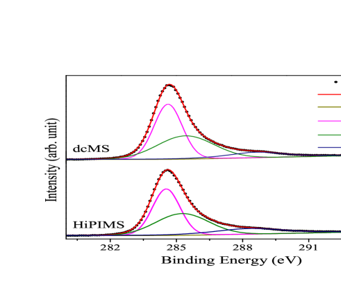
| Technique | dcMS | HiPIMS | ||
|---|---|---|---|---|
| Feature | BE (eV) | hyb.() | BE(eV) | hyb.() |
| sp2 | 284.6 | 48.1 | 284.6 | 44.2 |
| sp3 | 285.4 | 39.7 | 285.3 | 38.7 |
| C-O | 288.6 | 12.2 | 288.4 | 17.1 |
III.4 X-ray Absorption Near Edge Spectroscopy
X-ray absorption near edge spectroscopy (XANES) is one of the best technique to probe the local structure. C K-edge XANES spectra was measured in total electron yield mode. Samples deposited using dcMS and HiPIMS were measured under UHV conditions as shown in fig. 5. Pre and post-edge normalization has been applied using Athena software package Ravel and Newville (2005). The C K-edge spectra have several features assigned as , , , and . The feature a (285.5 eV) is due to 1s transition (or hybridization), the faint feature b is ambiguous and may be because of hybridization of carbon with nitrogen or hydrogen when exposed to atmosphere Hemraj-Benny et al. (2006), features and are due to hybridization of carbon with oxygen C-O and C=O, respectively and is because of hybridization. Comparing the films deposited with dcMS and HiPIMS, following difference are noteworthy (i) feature is more intense is dcMS deposited film (ii) features and are more intense in HiPIMS deposited film (iii) for HiPIMS deposited films we also find that the feature is almost absent and the feature is somewhat more prominent.
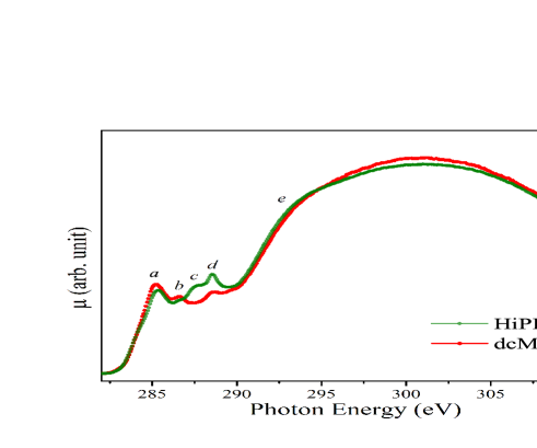
We find that the information obtained from C K-edge XANES measurements is in agreement with other results obtained in this work. Films deposited with HiPIMS have lower sp2 fractions and the most remarkable change can be seen in terms of significantly stronger C=O and C-O features ( and ). Since in both cases films were prepared under similar deposition conditions, it is unlikely that oxygen atoms get incorporated only in HiPIMS deposition process. From the AFM measurements (fig. 1) we can see that while dcMS deposited films have a rather smooth texture, those deposited with HiPIMS have particles about 5 times larger in the form of hillocks that are surrounded with a porous microstructure. Since the density of HiPIMS deposited films (obtained from NR measurements) is larger despite having a porous structure, it can be assumed that the hillocks formed here are dense and have a large sp3 fraction. Since in the HiPIMS process there is an enhancement in the ions, these ions not assist in nucleation of larger particles due to enhanced mobility but they may also bombard the growing film and lead to microstructure that is a combination of dense hillocks surrounded by pores. When samples are exposed to atmosphere those pores get filled with oxygen leading to a significant carbon oxygen bonding as observed by both XPS and XANES. We believe that by further tuning the deposition parameters in the HiPIMS process, the formation pores can be avoided or increased. In some applications in fact films with large porosity are required Laušević et al. (2013); Schopf and Es-Souni (2017). Such types of films have higher effective surface area that is desirable for high energy devices. In either way HiPIMS process offers a possibly to control the microstructure which is not generally possible in typical dcMS processes.
IV Conclusion
In this work we studied -C thin films deposited using dcMS and HiPIMS processes. The microstructure, electronic properties and the density of the films were measured. We show that while XRR have limitations in measuring small differences in the density of -C films due to poor scattering contrast and sample alignment. NR in ToF mode can be used for precise measurement of density of carbon thin films. Our results on the micro, electronic and film density correlate well and signify that HiPIMS process leads to formation of dense particles but at the same time bombardment of ions also increases pores. By further tuning the process it is believed that even denser and high sp3 fraction carbon thin films can be obtained by HiPIMS.
Acknowledgments
Authors would like to acknowledge Layanta Behera for help in sample preparation, V. R. Reddy and Anil Gome for XRR, Niti and Seema for NR, Rakesh Kumar Sah for XAS, Mohan Gangrade for AFM and Prakash Behara for XPS measurement. We are thankful to A. K. Sinha for support and encouragements. Authors thank the Department of Science and Technology, India (SR/NM/Z-07/2015) for the financial support and Jawaharlal Nehru Centre for Advanced Scientific Research (JNCASR) for managing the project.
References
References
- Robertson (2002) J. Robertson, Materials Science and Engineering: R: Reports 37, 129 (2002).
- Gaumet et al. (1993) J. J. Gaumet, A. Wakisaka, Y. Shimizu, and Y. Tamori, J. Chem. Soc., Faraday Trans. 89, 1667 (1993).
- Yamamoto et al. (1998) K. Yamamoto, Y. Koga, S. Fujiwara, F. Kokai, and R. Heimann, Applied Physics A 66, 115 (1998).
- Logothetidis et al. (1999) S. Logothetidis, M. Gioti, P. Patsalas, and C. Charitidis, Carbon 37, 765 (1999).
- Konstantinidis et al. (2006) S. Konstantinidis, J. Dauchot, and M. Hecq, Thin Solid Films 515, 1182 (2006), proceedings of the 33rd International Conference on Metallurgical Coatings and Thin Films.
- Lattemann et al. (2010) M. Lattemann, U. Helmersson, and J. Greene, Thin Solid Films 518, 5978 (2010).
- Lin et al. (2011) J. Lin, J. J. Moore, W. D. Sproul, and S. L. Lee, Journal of Vacuum Science & Technology A: Vacuum, Surfaces, and Films 29, 061301 (2011), http://dx.doi.org/10.1116/1.3645612 .
- Lattemann et al. (2011) M. Lattemann, B. Abendroth, A. Moafi, D. McCulloch, and D. McKenzie, Diamond and Related Materials 20, 68 (2011).
- Sarakinos et al. (2012) K. Sarakinos, A. Braun, C. Zilkens, S. Mráz, J. Schneider, H. Zoubos, and P. Patsalas, Surface and Coatings Technology 206, 2706 (2012).
- Nakao et al. (2013) S. Nakao, K. Yukimura, S. Nakano, and H. Ogiso, IEEE Transactions on Plasma Science 41, 1819 (2013).
- Huang et al. (2013) M. Huang, X. Zhang, P. Ke, and A. Wang, Applied Surface Science 283, 321 (2013).
- Lin et al. (2014) J. Lin, W. D. Sproul, R. Wei, and R. Chistyakov, Surface and Coatings Technology 258, 1212 (2014).
- Kimura and Kamata (2016) T. Kimura and H. Kamata, Japanese Journal of Applied Physics 55, 07LE02 (2016).
- Aijaz et al. (2016) A. Aijaz, S. Louring, D. Lundin, T. Kubart, J. Jensen, K. Sarakinos, and U. Helmersson, Journal of Vacuum Science & Technology A: Vacuum, Surfaces, and Films 34, 061504 (2016), https://doi.org/10.1116/1.4964749 .
- Ferrari et al. (2000a) A. C. Ferrari, A. Libassi, B. K. Tanner, V. Stolojan, J. Yuan, L. M. Brown, S. E. Rodil, B. Kleinsorge, and J. Robertson, Phys. Rev. B 62, 11089 (2000a).
- Liu et al. (2016) L. Liu, T. Wang, J. Huang, Z. He, Y. Yi, and K. Du, Diamond and Related Materials 70, 151 (2016).
- Wallace and Wu (1995) W. E. Wallace and W. L. Wu, Applied Physics Letters 67, 1203 (1995), https://doi.org/10.1063/1.115007 .
- Weiler et al. (1994) M. Weiler, S. Sattel, K. Jung, H. Ehrhardt, V. S. Veerasamy, and J. Robertson, Applied Physics Letters 64, 2797 (1994), http://dx.doi.org/10.1063/1.111428 .
- Stahn and Glavic (2016) J. Stahn and A. Glavic, Nuclear Instruments and Methods in Physics Research Section A: Accelerators, Spectrometers, Detectors and Associated Equipment 821, 44 (2016).
- Gupta et al. (2004) M. Gupta, T. Gutberlet, J. Stahn, P. Keller, and D. Clemens, Pramana 63, 57 (2004).
- Phase et al. (2014) D. M. Phase, M. Gupta, S. Potdar, L. Behera, R. Sah, and A. Gupta, AIP Conference Proceedings 1591, 685 (2014), http://aip.scitation.org/doi/pdf/10.1063/1.4872719 .
- Horcas et al. (2007) I. Horcas, R. Fernández, J. M. Gómez-Rodríguez, J. Colchero, J. Gómez-Herrero, and A. M. Baro, Review of Scientific Instruments 78, 013705 (2007), http://dx.doi.org/10.1063/1.2432410 .
- Ott (2007) F. Ott, Comptes Rendus Physique 8, 763 (2007).
- Penfold (2002) J. Penfold, Current Opinion in Colloid and Interface Science 7, 139 (2002).
- Ferrari et al. (2000b) A. C. Ferrari, A. Libassi, B. K. Tanner, V. Stolojan, J. Yuan, L. M. Brown, S. E. Rodil, B. Kleinsorge, and J. Robertson, Phys. Rev. B 62, 11089 (2000b).
- Patsalas et al. (2005) P. Patsalas, S. Logothetidis, and P. Kelires, Diamond and Related Materials 14, 1241 (2005), sMAC ’04 Conference Proceeding S.I.
- Parratt (1954) L. G. Parratt, Phys. Rev. 95, 359 (1954).
- Ansell et al. (1979) R. Ansell, T. Dickinson, A. Povey, and P. Sherwood, Journal of Electroanalytical Chemistry and Interfacial Electrochemistry 98, 79 (1979).
- Ravel and Newville (2005) B. Ravel and M. Newville, Journal of Synchrotron Radiation 12, 537 (2005).
- Hemraj-Benny et al. (2006) T. Hemraj-Benny, S. Banerjee, S. Sambasivan, M. Balasubramanian, D. A. Fischer, G. Eres, A. A. Puretzky, D. B. Geohegan, D. H. Lowndes, W. Han, J. A. Misewich, and S. S. Wong, Small 2, 26 (2006).
- Laušević et al. (2013) Z. Laušević, P. Y. Apel, J. B. Krstić, and I. V. Blonskaya, Carbon 64, 456 (2013).
- Schopf and Es-Souni (2017) D. Schopf and M. Es-Souni, Carbon 115, 449 (2017).