Split-gate device for indirect excitons
Abstract
We present a concept and experimental proof of principle for split-gate devices for indirect excitons (IXs). The split-gate forms a narrow channel, a point contact, for IX current. Control of IX flow through the split-gate with both gate voltage and excitation power is demonstrated.
Split-gates can be utilized for creating and controlling narrow channels (quantum point contacts) for electrons in mesoscopic electronic devices. Studies of electronic split-gate devices have led to a number of findings including electron focusing Sharvin1965 ; Sharvin1965a ; Tsoi1974 ; Houten1988 , conductance quantization Wees1988 ; Wharam1988 , electron beam collimation Molenkamp1990 ; Eriksson1996 ; Crook2000 , and electron flow branching Topinka2000 ; Topinka2001 .
In this work, we present a concept and proof-of-principle experiments with split-gate devices for indirect excitons (IXs). An IX is a bound pair of an electron and a hole in spatially separated layers, which can be realized in coupled quantum well (CQW) structures (Fig. 1a). Due to several advantageous properties, IXs form a system that can be used to explore transport of cold bosons through split-gate devices, providing a counterpart to the many transport studies of cold fermions through electronic split-gate devices. These properties include: (i) IXs have built-in dipole moments , allowing the control of IX energy by voltage, where the IX energy shifts as ( is the separation between the electron and hole layers, is voltage controllable electric field in the structure growth direction). Various in-plane potential landscapes formed by voltage for IXs were studied in earlier works, including excitonic ramps Hagn1995 ; Gartner2006 ; Dorow2016 , static Zimmermann1997 ; Zimmermann1998 ; Hammack2006 ; Remeika2012 ; Remeika2015 and moving Winbow2011 lattices, traps Huber1998 ; Gorbunov2004 ; High2009nl ; Schinner2013 ; Shilo2013 ; Mazuz-Harpaz2017 , and transistors Andreakou2014 . (ii) Long IX lifetimes allow them to travel long distances in mesoscopic devices before recombination Hagn1995 ; Gartner2006 ; Dorow2016 ; Remeika2012 ; Remeika2015 ; Winbow2011 ; Andreakou2014 . (iii) Long IX lifetimes also allow effective IX thermalization with the crystal lattice Butov2001 , giving the opportunity to study IX transport through mesoscopic devices in the quantum regime below the temperature of quantum degeneracy.
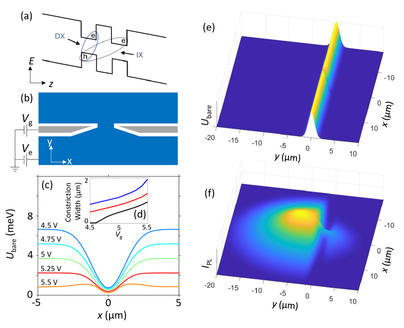
An excitonic split-gate device is formed by two electrodes: a large electrode (shown in blue (dark) in Fig. 1b) and a split-gate electrode (shown in gray in Fig. 1b). Voltage on the large electrode realizes the indirect regime in which IXs form the lowest energy state with energies below the energy of spatially direct excitons (DXs), which are also shown in Fig. 1a. Gate voltage on the split-gate electrode creates a narrow channel for IXs (Fig. 1c-f). The design of the IX split-gate device is similar to the design of electronic split-gate devices in semiconductor structures Houten1988 ; Wees1988 ; Wharam1988 ; Molenkamp1990 ; Eriksson1996 ; Crook2000 ; Topinka2000 ; Topinka2001 . A difference is in the presence of the large electrode, which is needed to implement the indirect regime for IX devices. This large electrode is separated from the split-gate electrode by a narrow opening. We note that in some IX CQW samples, e.g. in GaAs/AlAs CQW samples studied in Hagn1995 ; Huber1998 ; Hammack2006 , the indirect regime is realized at . Therefore, these samples don’t require a large electrode and, in turn, the narrow opening between it and the split-gate electrode, making the device design simpler.
The electric field and resulting IX potential energy for the bare, unscreened, split-gate device were modeled by numerically solving Poisson’s equation (note that the split-gate potential landscape and, in turn, are affected by IX screening, this is discussed below). Cross-sections of IX energy profiles at the split-gate position are shown in Fig. 1c for different . The IX energy is given relative to the energy of IXs far from the split-gate electrode, as determined by on the large electrode.
The channel width for transport of IXs with energy (relative to the IX energy in a bare device away from the split-gate) is controlled by . This is illustrated in Fig. 1d for a bare potential for several values. The control of split-gate channel by voltage provides control of IX current passing through. At low temperatures, is determined by IX interaction. IXs are oriented dipoles and interact repulsively with the interaction energy on the order of meV for typical IX densities Ivanov2002 ; Remeika2015 . The IX interaction energy for IX split-gate devices is analogous to the electron Fermi energy for electronic split-gate devices.
Figure 1e,f presents 3D images illustrating IX transport through a split-gate. IXs are generated by laser excitation on one side of the split-gate device (laser excitation centered around m is shown in Fig. 1f) and travel to the other side through the split-gate. This geometry corresponds to the experiments described below.
In the CQW structure grown by molecular beam epitaxy, an -GaAs layer with n cm-3 serves as a homogeneous bottom electrode. Two 8 nm GaAs QWs are separated by a 4 nm Al0.33Ga0.67As barrier and positioned 0.1 m above the -GaAs layer within an undoped 1 m thick Al0.33Ga0.67As layer. The QWs are positioned close to the homogeneous bottom electrode to suppress the in-plane electric field Hammack2006 , which could otherwise lead to IX dissociation Zimmermann1997 . The top semitransparent electrodes are fabricated by applying 2 nm Ti and 7 nm Pt.
IXs were generated by a 633 nm HeNe laser focused to a spot with full width half maximum m. Exciton photoluminescence (PL) was measured by a spectrometer and a liquid nitrogen cooled charge coupled device camera (CCD). The spatial – IX PL pattern was measured by the CCD after spectral selection by an nm interference filter chosen to match the IX energy. As a result, the low-energy bulk emission, higher-energy DX emission, and scattered laser light were effectively removed and the IX PL images were visualized. Experiments were performed in an optical helium cryostat at bath temperature K.
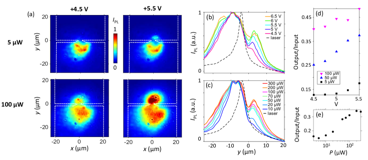
Experimental proof of principle for the IX split-gate device is shown in Fig. 2. IXs are photogenerated on one side of the split-gate (laser is positioned at (0,-4 m) in Fig. 2) and their transport through the split-gate is detected by measuring the spatial pattern of the IX emission. The rows in Fig. 2a and Figs. 2b and 2d show control of IX transport through the split-gate by gate voltage for a fixed laser excitation power . Increasing the channel width by voltage enhances the IX flux through the split-gate.
The columns in Fig. 2a and Figs. 2c and 2e show control of IX transport through the split-gate by laser excitation power for a fixed gate voltage . Increasing IX density by excitation power enhances the IX flux through the split-gate. This is described in terms of screening below.
We simulated IX transport through the split-gate in the diffusive regime corresponding to the proof of principle experiments shown in Fig. 2. This regime is characterized by the mean free path small compared to the device dimensions. The following nonlinear partial differential equation was used to model IX transport through the split-gate:
| (1) |
The first term in square brackets in Eq. 1 accounts for IX diffusion, is the IX density, the IX diffusion coefficient. The second term accounts for IX drift due to the dipole-dipole IX interaction, which is approximated by the plate capacitor formula , is the dielectric constant Ivanov2002 , and due to the split-gate potential . The IX mobility is given by the Einstein relation . The effect of in-plane disorder intrinsic to QWs is approximated using a “thermionic model” for the diffusion coefficient, Ivanov2002 . is the diffusion coefficient in the absence of QW disorder and is the amplitude of the disorder potential. The temperature of IXs is approximated as . The non-resonant photoexcitation causes heating of the IX gas by a few Kelvin. However, the hot IXs cool to the lattice temperature within few microns of the excitation spot Hammack2009 justifying the approximation. The last two terms in Eq. 1 account for the creation and decay of IXs. is the IX generation rate and is the IX lifetime.
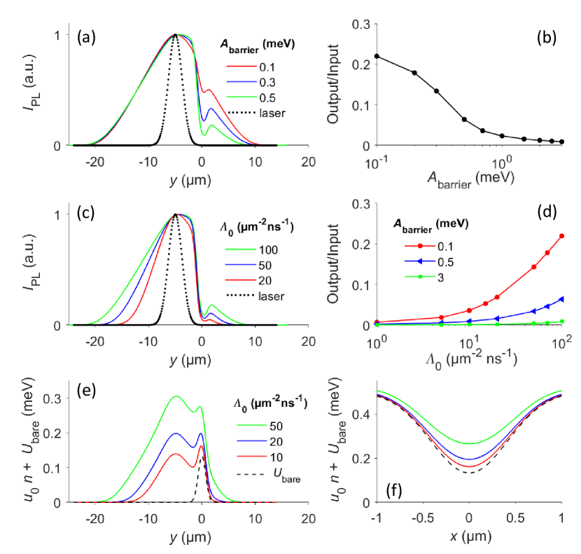
Simulations (Fig. 3) qualitatively reproduce both the control of IX transport through the split-gate by voltage (compare Fig. 2b with Fig. 3a and Fig. 2d with Fig. 3b) and by excitation power (compare Fig. 2c with Fig. 3c and Fig. 2e with Fig. 3d). The data are discussed below.
Increasing absolute value of gate voltage increases the channel width at the IX energy and also reduces the barrier height (Fig. 1c). As a result, IX transport through the split-gate is controlled by gate voltage (rows in Fig. 2a and Figs. 2b, 2d, 3a, and 3b). The dependence on voltage in simulations is presented by the dependence on the height of the bare barrier away from the channel (e.g. meV corresponds to V, see Fig. 1c).
Increasing IX excitation power increases IX density . This causes screening of the split-gate potential by IXs, increasing the channel width and reducing the barrier for IX transport through the split-gate (Figs. 3e and 3f). Increasing also causes screening of disorder as IXs interact repulsively. Screening of the split-gate potential and disorder increases IX transport through the split-gate (columns in Fig. 2a and Figs. 2c, 2e, 3c, and 3d).
An interesting regime for electron transport through electronic split-gates is the regime of quantum ballistic transport, where the mean free path and Fermi wavelength exceed the device dimensions. This regime is realized for electronic split-gate devices in high-quality semiconductor structures at low temperatures Houten1988 ; Wees1988 ; Wharam1988 ; Molenkamp1990 ; Eriksson1996 ; Crook2000 ; Topinka2000 ; Topinka2001 .
For excitonic devices, at low temperatures ( K, achievable in dilution refrigerators Butov2001 ; High2012 ), the IX coherence length in a coherent IX gas in high-quality CQW semiconductor structures reaches m High2012 , exceeding the dimensions of the split-gate channel (Fig. 1), IX interparticle separation ( m for typical IX density cm-2), and IX thermal de Broglie wavelength ( m for IX temperature K). This indicates the feasibility of the realization of IX quantum ballistic transport through excitonic split-gate devices at low temperatures. The realization of this regime forms the subject for future works.
We note that excitonic split-gate devices allow imaging IX current paths after spatially localized IX injection. Therefore, besides giving the opportunity to extend studies of narrow-channel phenomena in fermions Sharvin1965 ; Sharvin1965a ; Tsoi1974 ; Houten1988 ; Wees1988 ; Wharam1988 ; Molenkamp1990 ; Eriksson1996 ; Crook2000 ; Topinka2000 ; Topinka2001 to bosons, IX split-gate devices can also be used as a tool to probe directional effects in transport of composite bosons, including the predicted exciton Hall effect Dzyubenko1984 and exciton spin Hall effect Kavokin2005 . Excitonic split-gate devices can also be used for studying transport of composite particles through narrow channels Grasselli2016 .
In conclusion, we presented a concept and experimental proof of principle for split-gate devices for indirect excitons.
This work was supported by NSF Grant No. 1640173 and NERC, a subsidiary of SRC, through the SRC-NRI Center for Excitonic Devices. C. J. D. was supported by the NSF Graduate Research Fellowship Program under Grant No. DGE-1144086. This work used the Extreme Science and Engineering Discovery Environment (XSEDE), which is supported by NSF grant ACI-1548562, and XSEDE computer Comet at the San Diego Supercomputer Center through allocation TG-ASC150024.
References
- (1) Yu. V. Sharvin, A possible method for studying Fermi surfaces, J. Expt. Theor. Phys. 48, 984-985 (1965) [Sov. Phys. JETP 21, 655-656 (1965)]
- (2) Yu. V. Sharvin, L. M. Fisher, Observation of focused electron beams in a metal, Pisma ZhETF 1, 54-57 (1965) [JETP Lett. 1, 152-153 (1965)].
- (3) V. S. Tsoi, Focusing of electrons in a metal by a transverse magnetic field, Pisma ZhETF 19, 114-116 (1974) [Pisma JETP 19, 70-71 (1974)].
- (4) H. van Houten, B. J. van Wees, J. E. Mooij, C. W. J. Beenakker, J. G. Williamson, C. T. Foxon, Coherent Electron Focussing in a Two-Dimensional Electron Gas, Europhys. Lett. 5, 721-725 (1988).
- (5) B. J. van Wees, H. van Houten, C. W. J. Beenakker, J. G. Williamson, L. P. Kouwenhoven, D. van der Marel, C. T. Foxon, Quantized Conductance of Point Contacts in a Two-Dimensional Electron Gas, Phys. Rev. Lett. 60, 848-850 (1988).
- (6) D. A. Wharam, T. J. Thornton, R. Newbury, M. Pepper, H. Ahmed, J. E. F. Frost, D. G. Hasko, D. C. Peacockt, D. A. Ritchie, G. A. C. Jones, One-dimensional transport and the quantisation of the ballistic resistance, J. Phys. C: Solid State Phys. 21, L209-L214 (1988).
- (7) L. W. Molenkamp, A. A. M. Staring, C. W. J. Beenakker, R. Eppenga, C. E. Timmering, J. G. Williamson, C. J. P. M. Harmans, C. T. Foxon, Electron-beam collimation with a quantum point contact, Phys. Rev. B 41, 1274-1277 (1990).
- (8) M. A. Eriksson, R. G. Beck, M. Topinka, J. A. Katine, R. M. Westervelta, K. L. Campman, A. C. Gossard, Cryogenic scanning probe characterization of semiconductor nanostructures, Appl. Phys. Lett. 69, 671-673 (1996).
- (9) R. Crook, C. G. Smith, C. H. W. Barnes, M. Y. Simmons, D. A. Ritchie, Imaging diffraction-limited electronic collimation from a non-equilibrium one-dimensional ballistic constriction, J. Phys.: Condens. Matter 12, L167-L172 (2000).
- (10) M. A. Topinka, B. J. LeRoy, S. E. J. Shaw, E. J. Heller, R. M. Westervelt, K. D. Maranowski, A. C. Gossard, Imaging Coherent Electron Flow from a Quantum Point Contact, Science 289, 2323-2326 (2000)
- (11) M. A. Topinka, B. J. LeRoy, R. M. Westervelt, S. E. J. Shaw, R. Fleischmann, E. J. Heller, K. D. Maranowski, A. C. Gossard, Coherent branched flow in a two-dimensional electron gas, Nature 410, 183-188 (2001).
- (12) M. Hagn, A. Zrenner, G. Böhm, G. Weimann, Electric-field-induced exciton transport in coupled quantum well structures, Appl. Phys. Lett. 67, 232-234 (1995).
- (13) A. Gärtner, A.W. Holleitner, J.P. Kotthaus, D. Schuh, Drift mobility of long-living excitons in coupled GaAs quantum wells, Appl. Phys. Lett. 89, 052108 (2006).
- (14) C.J. Dorow, Y.Y. Kuznetsova, J.R. Leonard, M.K. Chu, L.V. Butov, J. Wilkes, M. Hanson, A.C. Gossard, Indirect excitons in a potential energy landscape created by a perforated electrode, Appl. Phys. Lett. 108, 073502 (2016).
- (15) S. Zimmermann, A.O. Govorov, W. Hansen, J.P. Kotthaus, M. Bichler, W. Wegscheider, Lateral superlattices as voltage-controlled traps for excitons, Phys. Rev. B 56, 13414-13421 (1997).
- (16) S. Zimmermann, G. Schedelbeck, A.O. Govorov, A. Wixforth, J.P. Kotthaus, M. Bichler, W. Wegscheider, G. Abstreiter, Spatially resolved exciton trapping in a voltage-controlled lateral superlattice, Appl. Phys. Lett. 73 154-156 (1998) .
- (17) A.T. Hammack, N.A. Gippius, Sen Yang, G.O. Andreev, L.V. Butov, M. Hanson, A.C. Gossard, Excitons in electrostatic traps, J. Appl. Phys. 99, 066104 (2006).
- (18) M. Remeika, M.M. Fogler, L.V. Butov, M. Hanson, A.C. Gossard, Two-dimensional electrostatic lattices for indirect excitons, Appl. Phys. Lett. 100, 061103 (2012).
- (19) M. Remeika, J.R. Leonard, C.J. Dorow, M.M. Fogler, L.V. Butov, M. Hanson, A.C. Gossard, Measurement of exciton correlations using electrostatic lattices, Phys. Rev. B 92, 115311 (2015).
- (20) A.G. Winbow, J.R. Leonard, M. Remeika, Y.Y. Kuznetsova, A.A. High, A.T. Hammack, L.V. Butov, J. Wilkes, A.A. Guenther, A.L. Ivanov, M. Hanson, A.C. Gossard, Electrostatic Conveyer for Excitons, Phys. Rev. Lett. 106, 196806 (2011).
- (21) T. Huber, A. Zrenner, W. Wegscheider, M. Bichler, Electrostatic Exciton Traps, Phys. Status Solidi A 166, R5-R6 (1998).
- (22) A.V. Gorbunov, V.B. Timofeev, Interwell Excitons in a Lateral Potential Well in an Inhomogeneous Electric Field, JETP Letters 80, 185–189 (2004) [Pis’ma Zh. Eksp. Teor. Fiz. 80, 210–215 (2004).
- (23) A.A. High, A.T. Hammack, L.V. Butov, L. Mouchliadis, A.L. Ivanov, M. Hanson, A.C. Gossard, Indirect Excitons in Elevated Traps, Nano Lett. 9, 2094-2098 (2009).
- (24) G.J. Schinner, J. Repp, E. Schubert, A.K. Rai, D. Reuter, A.D. Wieck, A.O. Govorov, A.W. Holleitner, J.P. Kotthaus, Confinement and Interaction of Single Indirect Excitons in a Voltage-Controlled Trap Formed Inside Double InGaAs Quantum Wells, Phys. Rev. Lett. 110, 127403 (2013).
- (25) Y. Shilo, K. Cohen, B. Laikhtman, K. West, L. Pfeiffer, R. Rapaport, Particle correlations and evidence for dark state condensation in a cold dipolar exciton fluid, Nat. Comm. 4, 2335 (2013).
- (26) Y. Mazuz-Harpaz, K. Cohen, B. Laikhtman, R. Rapaport, K. West, L.N. Pfeiffer, Radiative lifetimes of dipolar excitons in double quantum wells, Phys. Rev. B 95, 155302 (2017).
- (27) P. Andreakou, S.V. Poltavtsev, J.R. Leonard, E.V. Calman, M. Remeika, Y.Y. Kuznetsova, L.V. Butov, J. Wilkes, M. Hanson, A.C. Gossard, Optically controlled excitonic transistor, Appl. Phys. Lett. 104, 091101 (2014).
- (28) L.V. Butov, A.L. Ivanov, A. Imamoglu, P.B. Littlewood, A.A. Shashkin, V.T. Dolgopolov, K.L. Campman, A.C. Gossard, Stimulated Scattering of Indirect Excitons in Coupled Quantum Wells: Signature of a Degenerate Bose-Gas of Excitons. Phys. Rev. Lett. 86, 5608-5611 (2001).
- (29) A.L. Ivanov, Quantum diffusion of dipole-oriented indirect excitons in coupled quantum wells, Europhys. Lett. 59, 586-591 (2002).
- (30) A.T. Hammack, L.V. Butov, J. Wilkes, L. Mouchliadis, E.A. Muljarov, A.L. Ivanov, A.C. Gossard, Kinetics of the inner ring in the exciton emission pattern in coupled GaAs quantum wells, Phys. Rev. B 80, 155331 (2009).
- (31) A.A. High, J.R. Leonard, A.T. Hammack, M.M. Fogler, L.V. Butov, A.V. Kavokin, K.L. Campman, A.C. Gossard, Spontaneous coherence in a cold exciton gas, Nature 483, 584-588 (2012).
- (32) A.B. Dzyubenko, Yu.E. Lozovik, Quasi two-dimensional electron-hole pair condensate in a strong magnetics field, Fiz. Tverd. Tela 26, 1540-1541 (1984) [Sov. Phys. Solid State 26, 938 (1984)].
- (33) A. Kavokin, G. Malpuech, M. Glazov, Optical Spin Hall Effect, Phys. Rev. Lett. 95, 136601 (2005).
- (34) F. Grasselli, A. Bertoni, G. Goldoni, Exact two-body quantum dynamics of an electron-hole pair in semiconductor coupled quantum wells: A time-dependent approach, Phys. Rev. B 93, 195310 (2016).