Analytical Modeling of Metal Gate Granularity based Threshold Voltage Variability in NWFET 11footnotemark: 1
Abstract
Estimation of threshold voltage variability for NWFETs has been computationally expensive due to lack of analytical models. Variability estimation of NWFET is essential to design the next generation logic circuits. Compared to any other process induced variabilities, Metal Gate Granularity (MGG) is of paramount importance due to its large impact on variability. Here, an analytical model is proposed to estimate variability caused by MGG. We extend our earlier FinFET based MGG model to a cylindrical NWFET by satisfying three additional requirements. First, the gate dielectric layer is replaced by Silicon of electro-statically equivalent thickness using long cylinder approximation; Second, metal grains in NWFETs satisfy periodic boundary condition in azimuthal direction; Third, electrostatics is analytically solved in cylindrical polar coordinates with gate boundary condition defined by MGG. We show that quantum effects only shift the mean of the distribution without significant impact on the variability estimated by our electrostatics-based model. The distribution estimated by our model matches TCAD simulations. The model quantitatively captures grain size dependence with with excellent accuracy (error) compared to stochastic 3D TCAD simulations, which is a significant improvement over the state-of- the-art model with fails to produce even a qualitative agreement. The proposed model is faster compared to commercial TCAD simulations.
keywords:
NWFET, Metal Gate Granularity (MGG), Percolation, Threshold voltage (), Variability, Work function, Analytical model.1 Introduction
NWFET (Nanowire Field Effect Transistor) has emerged as the potential replacement for FinFET as an ultimate scaled CMOS device [1]. For both FinFET and NWFET, process induced variabilities have been very challenging from circuit performance viewpoint. Multi-gate transistors exhibit higher Metal Gate Granularity (MGG) variability compared other variability phenomena like Line Edge Roughness (LER), Random Dopant Fluctuation (RDF) etc., [2, 3, 4, 5]. The wider the distribution, the worse is the circuit performance [6]. Hence, the estimation of distribution is a must before circuit design.
It was reported that the NWFET (gate all around nanowire MOSFET) has better immunity against MGG induced variability compared to that of FinFET by 3D TCAD simulations in [7]. The smaller variability in NWFET is a strong motivation to replace FinFET with NWFET in future technology nodes. The steep computation cost of 3D stochastic TCAD simulations to extract variability seeks for more computationally efficient techniques. The distribution from smaller grain sizes typically result in a Gaussian like distribution while the larger grains produce a bimodal distribution (in case of two WF values). Any analytical method or model should be able to capture this size dependence efficiently. Further, analytical models are intuitive, faster than TCAD and can be a stepping-stone to a compact model. Recently, our group has developed the analytical estimation of the variability in FinFETs [8].
In this work, we extend the FinFET based MGG model to NWFET with cylindrical geometry by satisfying three additional constraints. The results from this model agree well with TCAD. Quantum confinement (not accounted in our model) produces a shift in the distribution without affecting its shape. The model is compared to state-of-the-art to show significant improvement achieved.
2 The Analytical Model
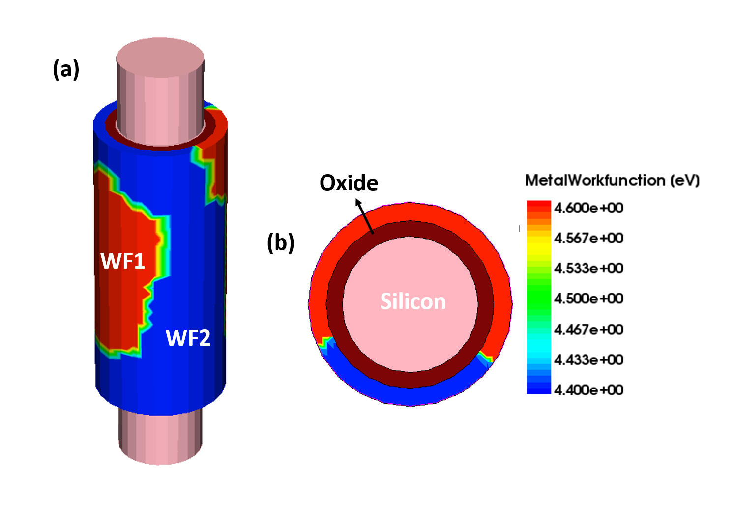
The body potential of NWFET is analytically modeled in [9, 10]. Due to very low free carrier concentration in sub-threshold regime, the electrostatics of the NWFET can be captured by the Laplace equation alone instead of Poisson equation [9]. A 3D schematic of the NWFET with MGG is shown in Fig.1(a). A simple cylinder is assumed for the purpose of solving the Laplace equation.
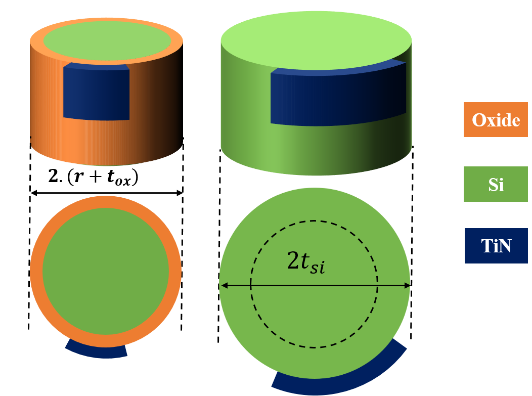
Two flat faces (planes) of the cylinder correspond to two boundary conditions (Source and the Drain) and the curved surface of the cylinder corresponds to the third boundary condition i.e. the Gate. The thin gate dielectric is substituted with electro-statically equivalent, thicker Silicon to form a single homogeneous cylinder. This simplification is essential for obtaining a closed form expression for the electrostatic potential. Due to this, the radius gets modified to effective (new) radius () and is given by (1).
| (1) |
where is the radius of the nanowire, is the diameter, and are the relative permittivities of the Silicon and the Oxide. The Gate length () remains unchanged. Due to this transformation, the actual grain gets stretched out only in the horizontal direction (azimuthal direction) by the factor as given by (1). This grain distortion is illustrated in Fig. 2. The procedure of finding variability in distribution is presented in three consecutive subsections below.
2.1 Cylindrical Gate MGG Generation
In this section, the algorithm for generating random metal gate grains is presented. This is similar to the algorithm used for FinFET in [8] except a grain periodicity constraint in the azimuthal direction. Since the gate is wrapped around the nanowire, metal grains on the NWFET gate satisfies the periodic boundary condition in azimuthal () direction for the Potential (). The modified algorithm is presented below. The average grain diameter () is assumed to vary from 3-25 nm [11]. The cut-open view of the gate is shown in Fig. 3(a).
-
1.
The mean number of grains () on the gate of a single NWFET is determined using
-
2.
The total gate area is discretized into a fine square mesh as shown in Fig. 3(a). Using ‘’ as the mean and standard deviation of the Poisson distribution, (assuming and is the grid size in and directions) random numbers are produced.
-
3.
These randomly generated integers are then assigned to every grid-point. The location of a non-zero integer is marked as grain center (red point) as seen in Fig. 3(a).
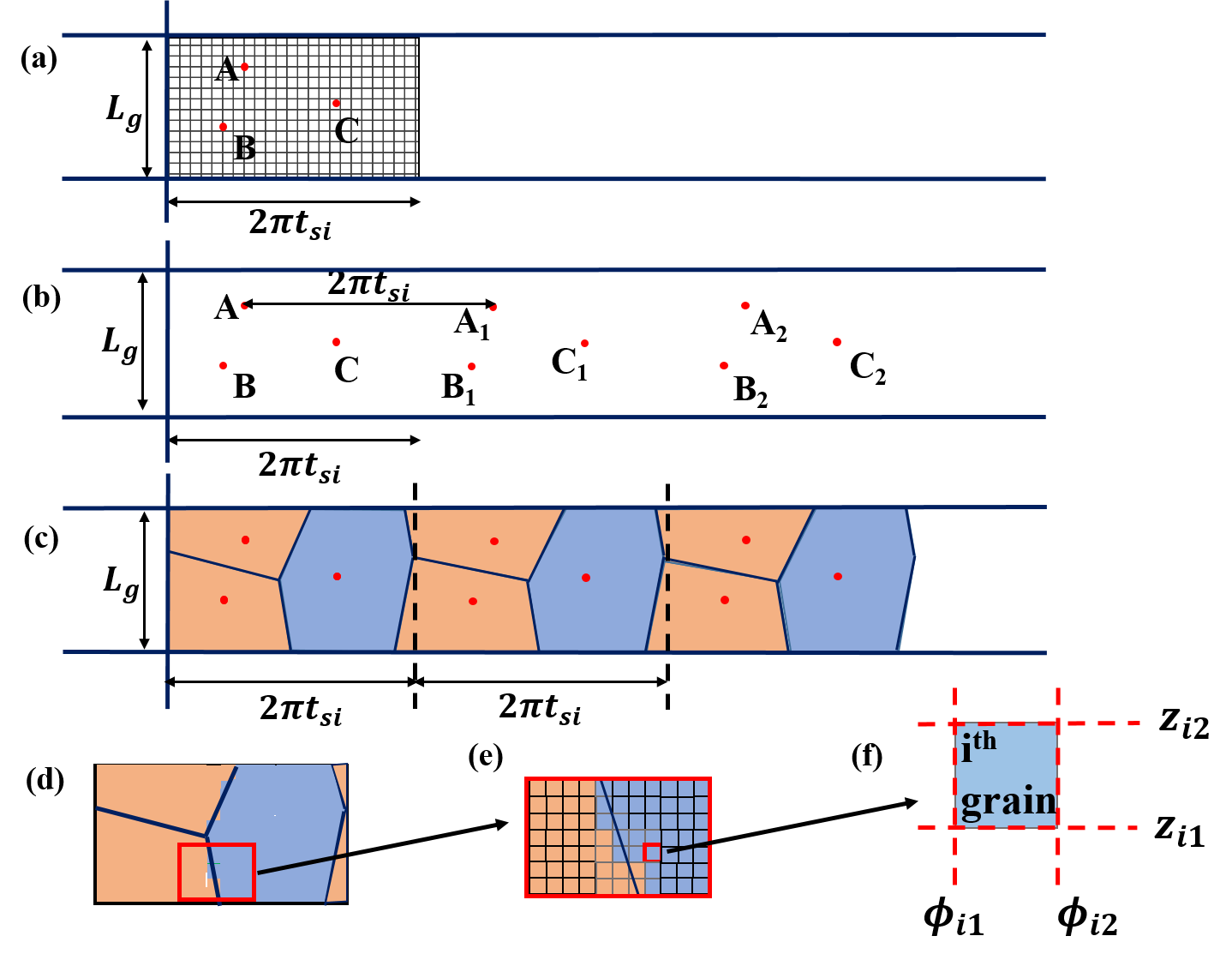
Figure 3: Methodology to assign boundary conditions on Gate. (a) Gate is discretized and using Poisson distribution, integers are generated randomly and assigned to every grid point. Non-zero integer locations are highlighted with red dots. (b) For each grain center, a point is marked at a distance of and another at and so on. (c) The blue solid lines represent perpendicular bisectors for the lines joining the dots. For each grain, WF is assigned based on probability. See the color assigned to each grain; (d) the marked section in figure (c) is selected as gate area. This selected area satisfies periodic boundary condition. (e) A representation of discretization a large Voronoi grain into tiny squares of appropriate WF; (f) The spatial coordinates (, , , ) of th grid point are shown. -
4.
For each grain center (say) ‘’ (see Fig. 3(b)), a grain center at a horizontal distance of is marked as and another at a distance of marked as and so on. The same procedure is followed for other grain centers and . (For the sake of simplicity only three grain centers are assumed in Fig. 3(a)). Thus, periodicity among grain centers is maintained.
- 5.
-
6.
The section marked by the black dashed lines in Fig.3(c) is then considered as the gate area to be wrapped around the NWFET. This procedure ensures periodic boundary condition for the potential of the gate area as seen in Fig. 3(d).
-
7.
The th grid-point corresponds to a square domain which lies between and . This domain is given the appropriate WF value (Fig. 3(e-f)) to make grains on NWFET as shown in Fig. 1(a).
Due to MGG, the WF vary randomly on the gate surface of NWFET. Depending on the material chosen for gate metal, the WF can take multiple values. For this work, TiN is assumed to be the gate metal.
2.2 Computing the Electrostatic Potential in the Nanowire
For solving the Laplace equation, the following boundary conditions for the cylinder are given below.
For the Gate:
| (2) |
For the Source:
| (3) |
For the Drain:
| (4) |
where is the applied gate bias, is the work-function (spatially varying) difference between gate material (TiN) and channel. is the work-function difference between the Source (or the Drain ) and channel and is the applied Drain bias.
The potential ( ) inside the nanowire requires contributions from the Gate, Source and, Drain. The potential due to Gate () is computed using (5) in MATLABTM whose derivation is adopted from [13] which solves Laplace equation in cylindrical coordinates unlike Cartesian coordinate in [8]. In the same way, the contribution of the Drain and the Source are computed using Eq. (6) and Eq. (7) adopted from [13]. The Fourier Bessel coefficients for the Gate are computed using (8) and (9). The total potential inside the nanowire at any point is the sum of all potentials from the Gate, the Source and, the Drain as given by equation (10) by simply following the Superposition principle.
| (5) |
| (6) |
| (7) |
| (8) |
| (9) |
| (10) |
where is the Modified Bessel function of order, and are the Bessel functions of zeroth and first order respectively. is the zero of the zeroth order Bessel function, and are the Fourier Bessel coefficients and are complex conjugates to each other as shown in (9). is the total number of grains on the gate area of a single device. is the boundary condition on the gate which varies spatially due to MGG.
2.3 Percolation model to estimate
estimation by resistance based percolation model is adopted from [14] in which local resistivity is computed from local potential by Eq. (11). The effective resistance is given by Eq. (12). This model is same as the percolation model used for FinFET in [8] except for geometry. The effective resistance is computed for each value (at a few regular intervals) of applied gate potential . We get exponentially decreasing values (and hence exponentially increasing current values computed using Eq. (13) ) as we increase values.
| (11) |
| (12) |
where is the potential at the Source end, is the doping in the Source and Drain region.
| (13) |
For each device, the sub-threshold I-V is estimated and hence, (by constant current method) value is extracted. The same process is followed and repeated for many devices (e.g. 250 NWFETs) to get values and the standard deviation () for the distribution of values can be computed.
3 Validation of the Proposed Model
The analytical model is corroborated with 3D TCAD simulations performed using Sentaurus. A sample structure used for stochastic simulations in TCAD is shown in Fig.1(a). The TCAD simulation deck uses Density Gradient Model [15] to account for quantization effects. The device and simulation parameters are calibrated according to the existing literature [16, 17]. First, electrostatic potentials are validated for few cases. Second, distributions obtained from analytical model are compared and validated against TCAD for different grain sizes. Finally, the standard deviations in distributions are compared to that of TCAD.
| Parameter | Value |
|---|---|
| Physical Gate Length () | |
| Nanowire diameter () | |
| Equivalent oxide thickness () | |
| Channel Doping | |
| S/D Doping | |
| WF for TiN for and respectively | |
| with probabilities 0.6 and 0.4 [11] | and |
3.1 Electrostatic potential validation with TCAD
In this section, the potential (cylindrical Laplace solution) obtained from the model is compared with TCAD 3D simulations (for and ). First, an NWFET with uniform gate WF (as shown in Fig. 4 (a)) displays good electrostatic potential agreement with TCAD , as seen in Fig. 4(c). Similarly, we show potential match for the non-uniform WF case (for the schematic of asymmetric WF grains as shown in Fig. 4(b)) in Fig. 4(d).
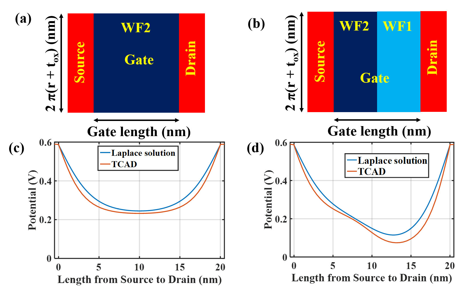
The asymmetry in WF (through the length of the device) is reflected in the asymmetry in the potential, which indicates that the positional dependence of the metal grains is accounted for. There seems to be a small quantitative mismatch in the potential. The gate oxide replacement, based on long cylinder approximation, is the primary reason for the mismatch in potential (near to Source or Drain, the tangential electric field dominates over the normal electric field). Along with that, use of finite basis functions in computation and assumption of metallic S/D also causes a mismatch in potential. Even so, the analytical Laplace solution is capable of capturing changes in the potential due to MGG qualitatively as shown in Fig. 4(d). This is essential to model for any arbitrary grain sizes, shape and distribution. The small quantitative errors in absolute potential produce a mean shift in distribution. Potential estimated using cylindrical Laplace solution is of decent accuracy by taking into account only first few harmonics of the sinusoidal functions (around 10 in number) and Modified Bessel functions (around 5 in number) for NWFET parameters given in Table 1.
3.2 Quantization effects on MGG induced variability
The quantum mechanical confinement effects due to narrow diameters in nanowires are not accounted for in our model. So, it is essential to have an estimate of error, if quantization is neglected. In TCAD, typically the Density Gradient (DG) model is activated in device simulations to account for this [15]. We compare the Classical Drift-Diffusion (DD) with DG corrected DD (DG + DD) stochastic 3D TCAD distributions of 5 nm and 20 nm grain sizes (Fig. 5).
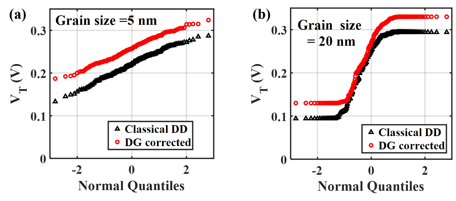
The distributions look identical except for the mean shift. From the Fig. 6(a), it is evident that standard deviation () is overestimated by 2 − 3 mV in the absence DG correction. The mean () however 20 − 30 mV shows a significant shift in distribution, which is expected [18]. This shows that, quantization shows a small effect on MGG induced variability as shown in Fig. 6(a), i.e. essentially an offset, without affecting the shape of the distribution (see Fig. 5).
We also present the statistics of sub-threshold slope (SS). The mean sub-threshold slope () values of DG corrected distributions are slightly (negligibly) higher (worse) compared to classical case. Both DD and DG+DD standard deviations () are much smaller compared to their respective mean values as shown in Fig. 6(b). Hence, the change in channeled via change in SS due to inclusion of DG is insignificant (see Fig. 6(c)). This shows that MGG either with or without DG correction has little impact on SS in NWFET, consistent with [3].
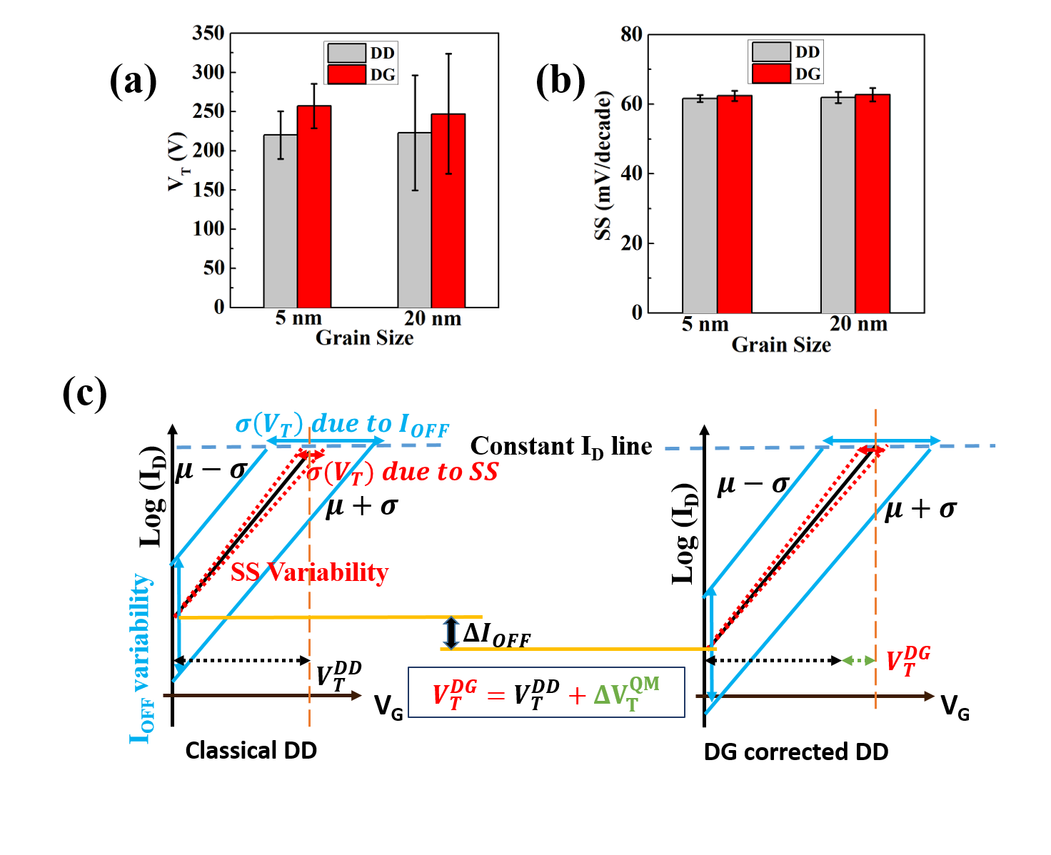
In comparison with FinFET reported in [8], the quantization effects on MGG induced variability is slightly higher for NWFET. In order to account for quantization effects in NWFET, a more elaborate method or model is necessary to introduce corrections in potential and charge density, which is beyond the scope of this work.
3.3 Comparison of distributions
First, stochastic 3D simulations of NWFETs with MGG are performed in SentaurusTM TCAD. The TCAD distributions are then compared with our model for four average grain sizes (3, 5, 7, 10, 15 and 20 nm) in Fig. 7.
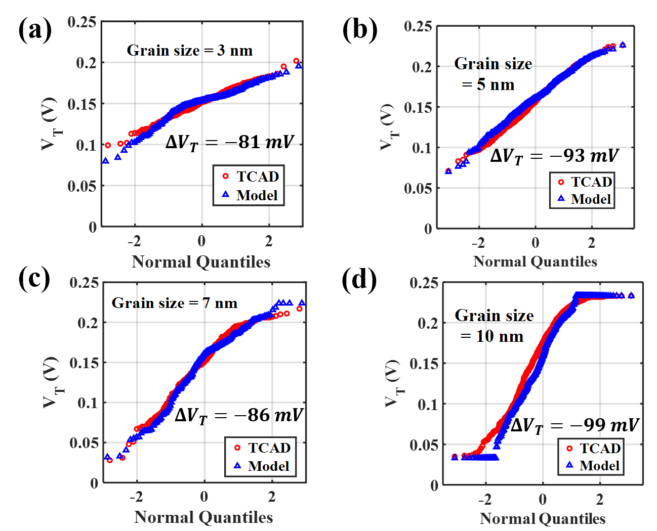
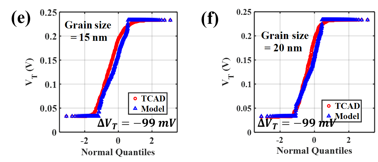
The mean () values of the distributions obtained from TCAD and proposed analytical model are different. So, for each distribution, an offset () is added to match the range of TCAD distribution. This alignment helps in better comparison of distributions with TCAD which can be observed in Fig. 7.
These simulations are performed only for . This is based on earlier TCAD simulation study on MGG in NWFET devices in [3] showed that the dependence of on is negligible.
As revealed by Fig. 7, the quantile plot resembles a Gaussian distribution for small grain sizes. However, for larger grain sizes (), the distributions are Gaussian but truncated by the extreme values. The extreme values differ by 200 mV which is equal to the WF differences in TiN. In other words, for large grains sizes, single WF gated devices (of either orientations) are more probable which is already reported in [3].The proposed analytical model can capture the shape of the distribution effectively for wide range of grain sizes i.e. Gaussian like distribution for smaller grain sizes and non- Gaussian for larger grain sizes.
3.4 Comparison of standard deviations of distributions
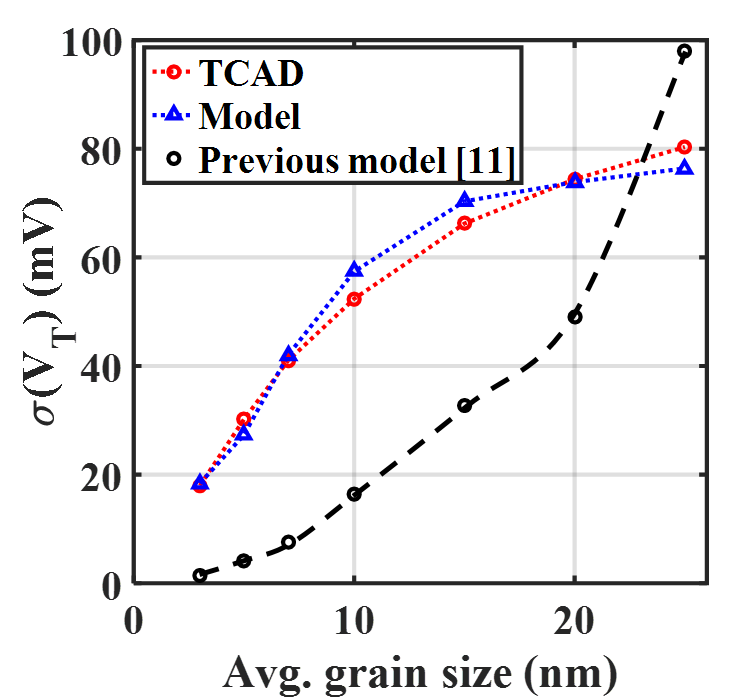
In this section, the s extracted from the analytical model are compared to TCAD 3D stochastic simulations (250 devices for every grain size). Both qualitative and quantitative match is observed in Fig. 8 between the model and the TCAD. For comparison, we also plotted the obtained using analytical model proposed earlier in [11]. The proposed analytical model gives about RMS error when compared with TCAD results. The relative error is small i.e. 6 compared to mean of over the range of grain sizes. Our analytical method is significantly () faster than TCAD ( On a computer with Intel XeonTM CPU E5620 (2.4 GHz × 16) processor with 64 GB of RAM).Thus, the proposed analytical model is reasonably accurate in prediction with high efficiency in computation.
4 Conclusion
MGG induced variability in NWFETs is estimated using electrostatics (along with percolation) based analytical modeling. The model successfully adapts the FinFET MGG model to cylindrical NWFET geometry with three modifications. They are 1) adoption of periodic boundary condition of gate potential in the azimuthal direction; 2) used long cylinder approximation to replace oxide with Silicon; 3) solved Laplace equations in cylindrical coordinate system. The distributions, and are validated with stochastic 3D TCAD simulations for different grain sizes. The effects of quantization although expected to be present at these dimensions, produces a shift in the distribution without affecting its shape. Thus, also remains unaffected. This model accurately captures the distribution for a large range of grain sizes (3-20 nm) – validated against 3D TCAD simulations. The dependence on grain size is quantitatively accurate, which is a significant improvement over the state-of-the-art, which is unable to capture qualitative trends. The proposed model has 63 × lesser computational cost when compared to stochastic 3D TCAD simulations. Such a model is able to capture the non-Gaussian distribution to enable accurate circuit simulation for device-circuit interactions.
References
References
- [1] K. J. Kuhn, Considerations for ultimate cmos scaling, IEEE Transactions on Electron Devices 59 (7) (2012) 1813–1828. doi:10.1109/TED.2012.2193129.
- [2] X. Wang, A. R. Brown, B. Cheng, A. Asenov, Statistical variability and reliability in nanoscale finfets, in: 2011 International Electron Devices Meeting, 2011, pp. 5.4.1–5.4.4. doi:10.1109/IEDM.2011.6131494.
- [3] K. Nayak, S. Agarwal, M. Bajaj, P. J. Oldiges, K. V. R. M. Murali, V. R. Rao, Metal-gate granularity-induced threshold voltage variability and mismatch in si gate-all-around nanowire n-mosfets, IEEE Transactions on Electron Devices 61 (11) (2014) 3892–3895. doi:10.1109/TED.2014.2351401.
- [4] N. Seoane, G. Indalecio, M. Aldegunde, D. Nagy, M. A. Elmessary, A. J. García-Loureiro, K. Kalna, Comparison of fin-edge roughness and metal grain work function variability in ingaas and si finfets, IEEE Transactions on Electron Devices 63 (3) (2016) 1209–1216. doi:10.1109/TED.2016.2516921.
- [5] X. Jiang, X. Wang, R. Wang, B. Cheng, A. Asenov, R. Huang, Predictive compact modeling of random variations in finfet technology for 16/14nm node and beyond, in: 2015 IEEE International Electron Devices Meeting (IEDM), 2015, pp. 28.3.1–28.3.4. doi:10.1109/IEDM.2015.7409787.
- [6] H. Dadgour, K. Endo, V. De, K. Banerjee, Modeling and analysis of grain-orientation effects in emerging metal-gate devices and implications for sram reliability, in: 2008 IEEE International Electron Devices Meeting, 2008, pp. 1–4. doi:10.1109/IEDM.2008.4796792.
- [7] H. Nam, Y. Lee, J. D. Park, C. Shin, Study of work-function variation in high- /metal-gate gate-all-around nanowire mosfet, IEEE Transactions on Electron Devices 63 (8) (2016) 3338–3341. doi:10.1109/TED.2016.2574328.
- [8] P. H. Vardhan, S. Mittal, S. Ganguly, U. Ganguly, Analytical estimation of threshold voltage variability by metal gate granularity in finfet, IEEE Transactions on Electron Devices 64 (8) (2017) 3071–3076. doi:10.1109/TED.2017.2712763.
- [9] B. Ray, S. Mahapatra, Modeling and analysis of body potential of cylindrical gate-all-around nanowire transistor, IEEE Transactions on Electron Devices 55 (9) (2008) 2409–2416. doi:10.1109/TED.2008.927669.
- [10] P. H. Vardhan, S. Mittal, A. S. Shekhawat, S. Ganguly, U. Ganguly, Analytical modeling of metal gate granularity induced vt variability in nwfets, in: 2016 74th Annual Device Research Conference (DRC), 2016, pp. 1–2. doi:10.1109/DRC.2016.7548446.
- [11] H. F. Dadgour, K. Endo, V. K. De, K. Banerjee, Grain-orientation induced work function variation in nanoscale metal-gate transistors; part i: Modeling, analysis, and experimental validation, IEEE Transactions on Electron Devices 57 (10) (2010) 2504–2514. doi:10.1109/TED.2010.2063191.
- [12] S. H. Chou, M. L. Fan, P. Su, Investigation and comparison of work function variation for finfet and utb soi devices using a voronoi approach, IEEE Transactions on Electron Devices 60 (4) (2013) 1485–1489. doi:10.1109/TED.2013.2248087.
- [13] J. D. Jackson, Electrodynamics, Wiley Online Library, 1975.
- [14] S. Mittal, A. S. Shekhawat, U. Ganguly, An analytical model to estimate finfet’s distribution due to fin-edge roughness, IEEE Transactions on Electron Devices 63 (3) (2016) 1352–1358. doi:10.1109/TED.2016.2520954.
- [15] Synopsys, Sentaurus Device User Guide, Synopsys Inc, 2015.
- [16] S. Mittal, S. Gupta, A. Nainani, M. C. Abraham, K. Schuegraf, S. Lodha, U. Ganguly, Epitaxially defined finfet: Variability resistant and high-performance technology, IEEE Transactions on Electron Devices 61 (8) (2014) 2711–2718.
- [17] N. Pons, F. Triozon, M.-A. Jaud, R. Coquand, S. Martinie, O. Rozeau, Y.-M. Niquet, V.-H. Nguyen, A. Idrissi-El Oudrhiri, S. Barraud, Density gradient calibration for 2d quantum confinement: Tri-gate soi transistor application, in: Simulation of Semiconductor Processes and Devices (SISPAD), 2013 International Conference on, IEEE, 2013, pp. 184–187.
- [18] H. Mehta, S. Lodha, U. Ganguly, S. Ganguly, Calibration of the density-gradient tcad model for germanium finfets, in: Micro and Nanoelectronics (RSM), 2013 IEEE Regional Symposium on, IEEE, 2013, pp. 143–146.